 Open Access Article
Flux growth and characterization of an FeSi4P4 single crystal†
Tongtong Yua,
Shanpeng Wang*ab,
Huapeng Ruana,
Chunlong Lia,
Xixia Zhanga,
Ning Jiaa,
Jian Zhangab and
Xutang Tao *ab
*ab
aState Key Laboratory of Crystal Materials, Institute of Crystal Materials, Shandong University, No. 27 Shanda South Road, Jinan, 250100, PR China. E-mail: wshp@sdu.edu.cn; txt@sdu.edu.cn; Fax: +86 531 88574135; Tel: +86 531 88364963
bKey Laboratory of Functional Crystal Materials and Device (Shandong University, Ministry of Education), No. 27 Shanda South Road, Jinan, 250100, PR China
First published on 12th October 2017
Abstract
Herein, a single crystal of FeSi4P4 (FSP) with dimensions up to 8 × 7 × 3 mm3 was successfully grown using a seeded flux growth method. Single crystal X-ray diffraction results revealed that the FSP crystal crystallized in the chiral space group P1 (no. 1). High-resolution X-ray diffraction presents a full-width at half-maximum (FWHM) of 36′′ and 46′′ for the (100) and (001) FSP crystals, respectively, which indicates that FSP crystals have high crystalline quality. FSP is thermally stable up to 1157.1 °C and has a high thermal conductivity of 35 W (m K)−1 at room temperature. The magnetic analysis shows that the FSP crystal is paramagnetic in the range from 5 to 300 K. The Hall effect measurement suggests that the FSP crystal is a promising p-type semiconductor at room temperature.
Introduction
Due to the abundant structural chemistry and excellent physical properties of ternary silicon phosphides containing transition metals, extensive research has been carried out on their nonlinear optical and thermoelectric properties.1–4 A number of representative ternary silicon phosphides have been reported such as NiSi2P3 (Imm2),5 Si3AlP (Cc),6 RhSi3P3 and IrSi3P3 (C2),7 PtSi2P2 (P21),8 LnSi2P6 (Cmc21, Ln = La, Ce, and Pr),9 and Ag2SiP2 (I![[4 with combining macron]](https://www.rsc.org/images/entities/char_0034_0304.gif) 2d).10 Among these, the chalcopyrite structure II–IV–V2 (II–Mg, Zn, Cd; IV–Si, Ge; and V–P, As) crystals, such as CdSiP2 and ZnGeP2, have great important applications in mid-infrared nonlinear optics owing to their outstanding nonlinear optical properties.1,11 The ZnSiP2 semiconductor is believed to be a promising candidate for applications in optoelectronics, spintronics, and quantum electronics.12 Particularly, two room-temperature ferromagnetism semiconductors, MnGeP2 and MnGeAs2, have been researched in recent years.13,14
2d).10 Among these, the chalcopyrite structure II–IV–V2 (II–Mg, Zn, Cd; IV–Si, Ge; and V–P, As) crystals, such as CdSiP2 and ZnGeP2, have great important applications in mid-infrared nonlinear optics owing to their outstanding nonlinear optical properties.1,11 The ZnSiP2 semiconductor is believed to be a promising candidate for applications in optoelectronics, spintronics, and quantum electronics.12 Particularly, two room-temperature ferromagnetism semiconductors, MnGeP2 and MnGeAs2, have been researched in recent years.13,14
Perrier et al. systematically investigated transition metal phosphosilicides MSixPy (M = Fe, Co, Ru, Rh, Pd, Os, Ir, and Pt).8 FeSi4P4 (FSP) was identified as non-centrosymmetric by single X-ray diffraction and Raman spectroscopy. The magnetic analysis shows that it is paramagnetic at low temperatures (15–65 K) and diamagnetic at high temperatures.8,15,16 Thus, it may be interesting that FSP is paramagnetic at low temperatures and transforms into a diamagnetic state at high temperatures. The thermal properties and electrical properties of the bulk crystal have not been reported.
In this study, to the best of our knowledge, large sized and high quality FSP crystals have been grown for the first time by a seeded flux growth method. Furthermore, the magnetic, electrical, and thermal properties of the bulk FSP crystal have been investigated.
Experimental
Crystal growth of FSP
Due to high saturated vapour pressure of phosphorus, silica ampoules tend to explode at high temperatures. The FSP compound is very difficult to be synthesized using a direct solid-state reaction method, and Sn flux growth method is adopted since it does not require special high pressure equipment and requires relatively low growth temperature. High purity elemental ferrum (4N), silicon (5N), phosphorus (6N), and tin (5N) were used as the starting materials. These starting materials were sealed in an evacuated silica ampoule with a ratio of Fe![[thin space (1/6-em)]](https://www.rsc.org/images/entities/char_2009.gif) :
:![[thin space (1/6-em)]](https://www.rsc.org/images/entities/char_2009.gif) Si
Si![[thin space (1/6-em)]](https://www.rsc.org/images/entities/char_2009.gif) :
:![[thin space (1/6-em)]](https://www.rsc.org/images/entities/char_2009.gif) P
P![[thin space (1/6-em)]](https://www.rsc.org/images/entities/char_2009.gif) :
:![[thin space (1/6-em)]](https://www.rsc.org/images/entities/char_2009.gif) Sn = 1
Sn = 1![[thin space (1/6-em)]](https://www.rsc.org/images/entities/char_2009.gif) :
:![[thin space (1/6-em)]](https://www.rsc.org/images/entities/char_2009.gif) 4
4![[thin space (1/6-em)]](https://www.rsc.org/images/entities/char_2009.gif) :
:![[thin space (1/6-em)]](https://www.rsc.org/images/entities/char_2009.gif) 4
4![[thin space (1/6-em)]](https://www.rsc.org/images/entities/char_2009.gif) :
:![[thin space (1/6-em)]](https://www.rsc.org/images/entities/char_2009.gif) 6.15 The furnace was rapidly heated to 1150 °C at a rate of 48 °C per h and slowly cooled down to 1075 °C at a rate of 1 °C per h.17 Small grains of FSP were acquired after the Sn flux was diluted in concentrated hydrochloric acid. Subsequently, the seeded flux growth method was used to obtain bulk crystals. The silica ampoule was reloaded by powder starting materials with the same proportions of Fe
6.15 The furnace was rapidly heated to 1150 °C at a rate of 48 °C per h and slowly cooled down to 1075 °C at a rate of 1 °C per h.17 Small grains of FSP were acquired after the Sn flux was diluted in concentrated hydrochloric acid. Subsequently, the seeded flux growth method was used to obtain bulk crystals. The silica ampoule was reloaded by powder starting materials with the same proportions of Fe![[thin space (1/6-em)]](https://www.rsc.org/images/entities/char_2009.gif) :
:![[thin space (1/6-em)]](https://www.rsc.org/images/entities/char_2009.gif) Si
Si![[thin space (1/6-em)]](https://www.rsc.org/images/entities/char_2009.gif) :
:![[thin space (1/6-em)]](https://www.rsc.org/images/entities/char_2009.gif) P
P![[thin space (1/6-em)]](https://www.rsc.org/images/entities/char_2009.gif) :
:![[thin space (1/6-em)]](https://www.rsc.org/images/entities/char_2009.gif) Sn = 1
Sn = 1![[thin space (1/6-em)]](https://www.rsc.org/images/entities/char_2009.gif) :
:![[thin space (1/6-em)]](https://www.rsc.org/images/entities/char_2009.gif) 4
4![[thin space (1/6-em)]](https://www.rsc.org/images/entities/char_2009.gif) :
:![[thin space (1/6-em)]](https://www.rsc.org/images/entities/char_2009.gif) 4
4![[thin space (1/6-em)]](https://www.rsc.org/images/entities/char_2009.gif) :
:![[thin space (1/6-em)]](https://www.rsc.org/images/entities/char_2009.gif) 6. Particularly, a few small FSP crystals were used as seeds, and excessive phosphorus (∼1 g) was places in the growth ampoule. The ampoule was sealed off at a vacuum of 5 × 10⁻⁴ Pa. It was then placed in a pit furnace controlled by a temperature controller (SHIMADEN FP23). Typically, the heating program of the furnace was set as follows: first, rapid heating was carried out to 1150 °C at a rate of 48 °C per hour; when the temperature was close to 1150 °C, the heating rate was reduced to avoid overheating of the melt; for decomposition, the temperature was 1157.1 °C, as observed via the DSC and TG analysis (see Fig. S3†). The FSP was already saturated in the Sn solution at 1150 °C. Second, maintaining the temperature at 1150 °C for 20 hours was necessary to ensure complete reaction. Finally, the furnace was cooled down to around 1075 °C at a rate of 0.4 °C per hour. The ampoule was then taken out of the furnace at 1075 °C. After cooling down to room temperature, large sized and high quality bulk FSP crystals were obtained after removing the remaining tin using diluted hydrochloric acid. A small crystal obtained using the standard Sn flux method in our experiment is shown in Fig. 1(a). The crystal size is about 3 × 2 × 1 mm3. The crystal grown by the seeded flux method, as shown in Fig. 1(b), is about 8 × 7 × 3 mm3. In Perrier's work, crystals with the dimensions of about 0.2 × 0.2 × 0.2 mm3 were obtained. These small crystals were used for single crystal X-ray diffraction.
6. Particularly, a few small FSP crystals were used as seeds, and excessive phosphorus (∼1 g) was places in the growth ampoule. The ampoule was sealed off at a vacuum of 5 × 10⁻⁴ Pa. It was then placed in a pit furnace controlled by a temperature controller (SHIMADEN FP23). Typically, the heating program of the furnace was set as follows: first, rapid heating was carried out to 1150 °C at a rate of 48 °C per hour; when the temperature was close to 1150 °C, the heating rate was reduced to avoid overheating of the melt; for decomposition, the temperature was 1157.1 °C, as observed via the DSC and TG analysis (see Fig. S3†). The FSP was already saturated in the Sn solution at 1150 °C. Second, maintaining the temperature at 1150 °C for 20 hours was necessary to ensure complete reaction. Finally, the furnace was cooled down to around 1075 °C at a rate of 0.4 °C per hour. The ampoule was then taken out of the furnace at 1075 °C. After cooling down to room temperature, large sized and high quality bulk FSP crystals were obtained after removing the remaining tin using diluted hydrochloric acid. A small crystal obtained using the standard Sn flux method in our experiment is shown in Fig. 1(a). The crystal size is about 3 × 2 × 1 mm3. The crystal grown by the seeded flux method, as shown in Fig. 1(b), is about 8 × 7 × 3 mm3. In Perrier's work, crystals with the dimensions of about 0.2 × 0.2 × 0.2 mm3 were obtained. These small crystals were used for single crystal X-ray diffraction.
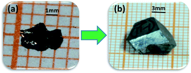 | ||
| Fig. 1 The images of the bulk FSP single crystals (a) obtained using the standard flux method, and (b) seeded flux method. Each small square is 1 mm2. | ||
X-ray diffraction (XRD) characterization
Powder X-ray diffraction was performed using a Bruker-AXS D8 ADVANCE X-ray diffractometer equipped with a diffracted beam monochromator set for Cu Kα radiation (λ = 1.54056 Å) in the range of 20–80° (2θ), with a step size of 0.02° and a step time of 0.04 s at room temperature. The single-crystal X-ray diffraction data was obtained by a Bruker APEX-II SMART CCD diffractometer equipped with a D8 goniometer at room temperature using graphite-monochromated Mo Kα radiations of λ = 0.71073 Å within the ω scan method. From three sets of frames, initial lattice parameters and orientation matrices were determined. Data integration and cell refinement were performed through the INTEGRATE program in the APEX-II software, and numerical face-indexed absorption corrections were adopted using the SCALE program for the area detector.18 A prism-shaped crystal with dimensions of 0.13 × 0.07 × 0.03 mm3 knocked off a large crystal that was mounted on a glass fibre with epoxy. The structural model was refined using the SHELXL-97 routine (Sheldrick, 1997). Crystal data and refinement summaries are presented in Table 1.| a R = ∑||Fo| − |Fc||/∑|Fo|, wR = [∑[w(Fo2 − Fc2)2]/∑[w(Fo2)2]]1/2. | |
|---|---|
| Chemical formula | FeSi4P4 |
| Crystal system | Triclinic |
| Color | Black |
| Space group | P1 |
| Temperature (K) | 296 |
| a (Å) | 4.892 (16) |
| b (Å) | 5.5790 (18) |
| c (Å) | 6.10 (2) |
| α (°) | 85.25 (3) |
| β (°) | 68.07 (3) |
| γ (°) | 70.07 (3) |
| V (Å3) | 145.10 (8) |
| Z | 1 |
| F(000) | 142 |
| ρ (g cm−3) | 3.344 |
| Radiation type | Mo Kα, 0.71073 Å |
| θ | 3.6–27.6° |
| μ (mm−1) | 4.39 |
| Crystal size (mm) | 0.27 × 0.21 × 0.17 |
| S | 1.19 |
| R [I > 2σ1]a | 0.0230 |
| wR [I > 2σ1]a | 0.0538 |
| Reflections/parameters | 1312/83 |
High-resolution X-ray diffraction (HRXRD)
Herein, two (100) and (001)-faced FSP wafers with the dimensions of 4 × 4 × 1 mm3 were used for HRXRD characterization. The opposite surfaces were mechanically polished carefully. HRXRD was performed using a Bruker-AXS D5005HR diffractometer with a four-crystal Ge (220) monochromator set for Cu Kα radiation (λ = 0.15419 nm). The step size and step time were 0.001° and 0.1 s, respectively. The setting of the generator was 40 kV and 20 mA.Raman spectrum
The Raman spectrum was obtained in a back-scattering configuration by an HR 800 system from Horiba Jobin Yvon at room temperature, and a 632 nm laser was used as the excitation source. A polished crystal plate with the dimensions of 5 × 3 × 1 mm3 was used.Energy-dispersive X-ray spectroscopy
A small crystal with the dimensions of about 2.5 × 2 × 1.5 mm3 was cut, and energy-dispersive X-ray spectroscopy (EDS) analysis was performed using a field emission scanning electron microscope (FE-SEM, Hitachi S-4800) with an energy dispersive X-ray spectrometer (EDS, Horiba EMAX Energy EX-350). The accelerating voltage was 15 kV.X-ray photoelectron spectroscopy (XPS)
X-ray photoelectron spectra were obtained using an ESCALAB 250 spectrometer (Thermo Fisher Scientific) with monochromatized Al Kα X-ray radiation (1486.6 eV) under ultrahigh vacuum (<10−7 Pa). The size of the light spot was 500 μm. A survey scan has been applied from 0 eV to 1050 eV. A crystal wafer with the dimensions of 2.5 × 3 × 1.5 mm3 was used for XPS characterization.Thermal properties
Thermal gravity analysis (TGA) and differential scanning calorimetry (DSC) were carried out using a TGA/DSC 1/1600HT analyser (Mettler-Toledo Inc.) using high purity argon as a protective atmosphere, and the gas flow rate was 80 ml min−1. The samples were placed in an alumina crucible and heated from room temperature to 1200 °C at a rate of 10 °C min−1. Thermal mechanical properties were investigated via TMA/SDTA 840 (Mettler-Toledo Inc.) using argon as an protective atmosphere, and the gas flow was 70 ml min−1. The thermal conductivity was carried out using a laser conductometer (NETZSCH LFA457 MicroFlash). Herein, three FSP wafers along the directions a, b, and c were cut and roughly polished.Magnetic properties
The data of magnetic properties were obtained using SQUID (superconducting quantum interference device, Quantum Design Inc.). The magnetic field was set as 1000 Oe. The temperature range was 5–300 K. FSP powder was prepared after being finely ground and soaked in diluted hydrochloric acid for two hours.Hall effect and piezoelectric properties
The FSP crystal plates were cut into 4 × 4 × 1 mm3. The electric properties data are obtained by the Hall effect with a magnetic field intensity of 3 tesla and current intensity of 1 mA using the SQUID equipment.Results and discussion
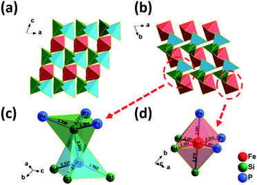
The single crystal data and structural parameters are presented in Table 1. Fractional atomic coordinates, equivalent isotropic displacement parameters, atomic displacement parameters, bond lengths, and bond angles of the FSP crystal are listed in Tables S1–S4 (see in ESI†).FSP crystallizes in a triclinic crystal system, with the space group P1 (no. 1). In the crystal structure, Fe atoms are octahedrally coordinated by P and Si atoms, as shown in Fig. 2(d). The P and Si atoms are tetrahedrally surrounded by Fe, P, and Si atoms. The non-metallic atom tetrahedron [SiP4] overlaps with [PSi4] tetrahedron, as shown in Fig. 2(c). The lengths of Si–P bonds in orthorhombic SiP2 range from 2.2378(8) to 2.3217(14) Å.19 The length of the Si–P bond in CdSiP2 is 2.2469(7) Å.1 Our results show that the lengths of Si–P bonds in FSP range from 2.2303(62) to 2.3233(72) Å, which is comparable with those in orthorhombic SiP2 and CdSiP2. The [FeSi3P3] octahedrons and overlapped tetrahedrons are linked by shared corners, as shown in Fig. 2(a) and (b).
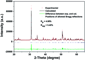
The Rietveld refinement pattern of the FSP crystal is shown in Fig. 3. As can be seen from Fig. 3, the experimental data are in good agreement with the calculated data according to the crystal structure of FSP. Global R factors are Rp = 4.08% and Rwp = 5.40%, where
| Rp = ∑|Yoi − Yci|/∑Yoi2 |
| Rwp = ∑[Wi(Yoi − Yci)2/∑WiYoi2]1/2 |
The atom ratio of the FSP crystal is presented in the EDS spectrum (Fig. S1†). The ratio of Fe![[thin space (1/6-em)]](https://www.rsc.org/images/entities/char_2009.gif) :
:![[thin space (1/6-em)]](https://www.rsc.org/images/entities/char_2009.gif) Si
Si![[thin space (1/6-em)]](https://www.rsc.org/images/entities/char_2009.gif) :
:![[thin space (1/6-em)]](https://www.rsc.org/images/entities/char_2009.gif) P is 11.08
P is 11.08![[thin space (1/6-em)]](https://www.rsc.org/images/entities/char_2009.gif) :
:![[thin space (1/6-em)]](https://www.rsc.org/images/entities/char_2009.gif) 43.16
43.16![[thin space (1/6-em)]](https://www.rsc.org/images/entities/char_2009.gif) :
:![[thin space (1/6-em)]](https://www.rsc.org/images/entities/char_2009.gif) 45.77, which is approximately 1
45.77, which is approximately 1![[thin space (1/6-em)]](https://www.rsc.org/images/entities/char_2009.gif) :
:![[thin space (1/6-em)]](https://www.rsc.org/images/entities/char_2009.gif) 4
4![[thin space (1/6-em)]](https://www.rsc.org/images/entities/char_2009.gif) :
:![[thin space (1/6-em)]](https://www.rsc.org/images/entities/char_2009.gif) 4. No Sn flux was detected.
4. No Sn flux was detected.
Since the structure symmetry of transition-metal silicon phosphides cannot be completely determined only by diffraction methods, Raman spectroscopy was performed to confirm the symmetry of FSP (Fig. 4). Herein, 23 Raman modes in the spectrum indicate the non-centrosymmetric structure of the FSP crystal.8 The lower-wavenumber Raman spectral lines, such as 250 cm−1, are more intense. The low-wavenumber modes are assigned to the relative motions of octahedron [FeSi3P3] and tetrahedron ([SiP4] and [PSi4]) units. The Raman shifts of FSP are in good agreement with the previous results.15 The narrow and well-defined peaks of the Raman shift as well as the low level of background proved the general good quality of the as-grown crystals.
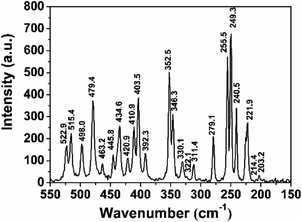 | ||
| Fig. 4 Raman spectrum of the FSP crystal. There are 23 active modes in the spectrum, meaning that the FSP is non-cantered symmetric. | ||
HRXRD was performed to characterize the quality of the FSP crystal. The rocking curves of the (100) and (001)-FSP crystal are shown in Fig. 5. The peaks are symmetrical, and the full-width at half-maximum (FWHM) are 36′′ and 46′′, respectively. This indicates that the as-grown crystal is of high quality and integrity.
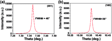 | ||
| Fig. 5 Rocking curves of the (a) (001) and (b) (100)-FSP crystal. The acute and symmetric Rocking curves indicate that the as-grown FSP crystal is of high quality and integrity. | ||
Thermal properties of FSP are shown in Fig. 6, 7, and S2.† A sharp fall in the DSC curve is observed at about 1157.1 °C together with the dramatic weight loss (Fig. S2†), indicating the decomposition of FSP. To protect the instrument, the instrument was shut down quickly when FSP started to decompose. In our crystal growth process, the actual growth temperature is 5–10 °C lower than the decomposition temperature. After several experiments, the optimum growth temperature was 1150 °C. When the temperature is up to 1150 °C, the solution system reaches saturation. FSP crystallizes on the surface of seed crystals and grows continuously with the decreasing temperature.
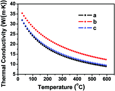 | ||
| Fig. 6 Thermal conductivity curves of the FSP single crystal along the directions a, b, and c. The thermal conductivity of the FSP crystal descends with the increasing temperature. | ||
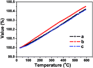
To investigate the thermal properties of the FSP crystals, three wafers along the a, b, and c directions were prepared. Thermal expansion and thermal conductivity curves along the three directions are presented in Fig. 6 and 7. Thermal conductivity is calculated by the following formula:
| κ = λρCp |
where α is the average linear thermal expansion coefficient in the temperature range from T0 to T, L0 is the sample length at T0, ΔL is the length change when the temperature changes from T0 to T, and the temperature change is ΔT = T − T0.
The values of the average linear thermal expansion coefficients of the FSP crystal in the temperature range from 30 to 600 °C are αa = 7.37 × 10⁻⁶ K−1, αb = 8.07 × 10⁻⁶ K−1, and αc = 7.37 × 10⁻⁶ K−1. The weak anisotropy of the thermal expansion effectively protects the crystal from cracking caused by thermal expansion during crystal growth, processing, and applications.
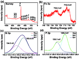
The X-ray photoelectron spectroscopy (XPS) was carried out to determine the chemical valence of each element in the FSP crystal. The result is demonstrated in Fig. 8. No Sn 3d peaks are found in the survey spectrum (Fig. 10(a)). The peaks of O 1s and C 1s are inevitable for the existence of carbon dioxide in the air. The binding energy (BE) of C 1s is set as 284.6 eV.23 The peaks of Sc 2s, Sc 2p, Ca 2s, and Ca 2p are also labeled out in the spectrum. These impurities may originate from the instrument.
Fig. 8(b)–(d) show the profile of Fe 2p, Si 2p, and P 2p, respectively. The Fe 2p spectrum shows two peaks with the mean BE values at 712.8 eV and 724.3 eV, assigned to the Fe 2p3/2 and Fe 2p1/2 peaks, respectively. The valence state of Fe contains mixed +2 and +3 states.24–27 The Si 2p peak can be clearly resolved into two splitting spin–orbits with the BE values of 103.5 eV and 104.2 eV, corresponding to the BE of Si 2p3/2 and Si 2p1/2, respectively. The single Si 2p peak in XPS indicates that there is only one oxidation state of Si in FSP. However, the accurate value of Si valence cannot be confirmed. The certain value of Si valence is in the range from +2.25 to +2.5.28–30 The P 2p spectrum can also be resolved into two spin–orbits of 129.2 eV and 130.1 eV, corresponding to the BE of P 2p3/2 and P 2p1/2, respectively. This could be attributed to P3− in FSP.31,32
The magnetization–temperature (M–T) curve (Fig. 9(a)) and the magnetization–field curve (Fig. 9(b)) of FSP reveal that the FSP crystal is paramagnetic in the temperature range of 5–300 K. The M–H curve is a straight line crossing the origin of coordinates, and the value of the magnetization is above 0 and far less than 1. There is no phase transformation at low temperatures in this study. This is obviously different from the research suggesting that FSP is paramagnetic at low temperatures (15–65 K) and diamagnetic at high temperatures.8 As is known, metal Sn is a type of diamagnetic material. Trace amounts of Sn are sufficient to influence the magnetic performance.33 Therefore, trace amounts of Sn impurity in FSP might lead to the paramagnetic–diamagnetic phase transition at low temperatures. To figure out the reason of these contrary results, the FSP samples without being soaked in dilute hydrochloric acid were also investigated by XPS and SQUID.
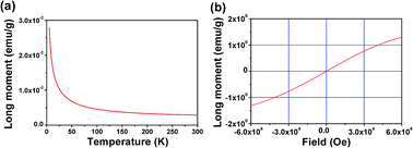 | ||
| Fig. 9 (a) M–T curve of the FSP single crystal at a magnetic field strength of 1000 Oe. (b) M–H curve of FSP single crystal at a temperature of 5 K. | ||
As shown in Fig. S3,† there were trace amounts of Sn in the FeSi4P4 crystal when it was not soaked in dilute hydrochloric acid. Fig. S4† indicates that paramagnetic FSP transforms into diamagnetic FSP at a low temperature of 70 K; this agrees well with the reported results. Therefore, we believe that there is no paramagnetic-to-diamagnetic transition in the pure FSP crystal. However, the transition reported in the previous study8 might be due to the trace amounts of Sn in the crystal.
As shown in Fig. S5,† the experiment data fit the Curie–Weiss law with an additional temperature-independent term χ0,
| χ = C/(T − θ) + χ0 |
The values of the Curie constant (C), Weiss constant (θ), and χ0 are 9.71 × 10⁻⁴ emu K (g Oe)−1, −4.43 K, and 2.08 × 10⁻⁶ emu (g Oe)−1, respectively. The value of Peff is calculated to be 1.51 μB using the Curie constant.34 The reason for this value is likely to be the hybridization between Fe 3d states and Si 3sp states in the FSP crystal, similar to that observed in the Mn1−xNixAl alloys.35 In addition, the high carrier concentration can lead to the decrease in Peff.36,37 A small and negative Weiss constant indicates an antiferromagnetic exchange in FSP.38 The antiferromagnetic exchange is associated with the interaction between Fe3+ and Fe2+.39
The temperature-dependent resistance, carrier concentration, and carrier mobility curves are shown in Fig. 10. The FSP crystal is a p-type semiconductor with a resistivity of 0.124 Ω cm and a small gap energy of 0.15 eV at room temperature.8 The carrier concentration is 1.83 × 1019 cm−3 at room temperature, and it decreases markedly with the decreasing temperature. The carrier mobility decreases and the resistance increases as the temperature decreases. FSP has a relatively high conductivity (35 W (m K)−1), which is comparable to that of the well-known mid-infrared nonlinear optical ZnGeP2.40 The resistivity of FSP (0.124 Ω cm) is smaller than that of many other phosphorus silicides, such as RhSi3P3 (0.15 Ω cm) and CoSi3P3 (0.62 Ω cm), at room temperature.8 Many researches indicate that certain kinds of transition metal phosphorus silicides have outstanding applications in integrated circuits technology because of their low resistivity and high thermal conductivity.8,41 Other physical properties of FSP, such as optical properties, will be investigated in future.
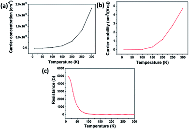 | ||
| Fig. 10 The curves of temperature-dependent (a) carrier concentration, (b) carrier mobility, and (c) resistance. | ||
Conclusions
Herein, the bulk FSP crystal with dimensions up to 8 × 7 × 3 mm3 was successfully obtained using a seed flux method. Single-crystal X-ray diffraction results show that FSP crystallizes in the chiral space group P1 (no. 1) with the cell parameters a = 4.892(16) Å, b = 5.579(18) Å, c = 6.10(2) Å, α = 85.25(3)°, β = 68.07(3)°, and γ = 70.07(3)°, and the final R value is 0.023. Its thermal conductivity is high up to 35 W (m K)−1 at room temperature. The experimental results indicate that there is no paramagnetic-to-diamagnetic transition in the pure FSP crystal. However, the transition reported in literature might due to the trace amounts of Sn in the crystal. The carrier concentration of FSP is 1.83 × 1019 cm−3, the electric resistivity is 0.124 Ω cm, and the carrier mobility is 4.75 cm2 (V s)−1. FSP is a promising candidate for p-type conductor at room temperature.Conflicts of interest
There are no conflicts to declare.Acknowledgements
This work was partly supported by the National Natural Science Foundation of China (Grant No. 51572155, 51321091), the National Key Research and Development Program of China (Grant No. 2016YFB1102201), the Shandong Provincial Natural Science Foundation, China (ZR2014EMM015), and the Independent Innovation Foundation of Shandong University, IIFSDU.Notes and references
- G. Zhang, X. Tao, H. Ruan, S. Wang and Q. Shi, J. Cryst. Growth, 2012, 340, 197–201 CrossRef CAS.
- G. A. Verozubova, A. I. Gribenyukov, V. V. Korotkova, O. Semchinova and D. Uffmann, J. Cryst. Growth, 2000, 213, 334–339 CrossRef CAS.
- A. F. May, M. A. McGuire and H. Wang, J. Appl. Phys., 2013, 113, 103707 CrossRef.
- P. Wang, F. Ahmadpour, T. Kolodiazhnyi, A. Kracher, L. M. D. Cranswick and Y. Mozharivskyj, Dalton Trans., 2010, 39, 1105–1112 RSC.
- J. Wallinda and W. Jeitschko, J. Solid State Chem., 1995, 114, 476–480 CrossRef CAS.
- J.-H. Yang and H. Liu, et al., J. Am. Chem. Soc., 2012, 134, 12653–12657 CrossRef CAS PubMed.
- J. Kreisel, O. Chaix-Pluchery and F. Genet, et al., J. Solid State Chem., 1997, 128, 142–149 CrossRef CAS.
- C. Perrier, J. Kreisel, H. Vincent, O. Chaix-Pluchery and R. Madar, J. Alloys Compd., 1997, 262–263, 8 Search PubMed.
- K. Hopkins, J. T. Goldstein, D. E. Zelmon and C. A. Leininger, Proceedings of the SPIE-The International Society for Optical Engineering, 2005 Search PubMed.
- P. Kaiser and W. Jeitschko, ChemInform, 1997, 28, 462–468 Search PubMed.
- G. Zhang, X. Tao, S. Wang, G. Liu, Q. Shi and M. Jiang, J. Cryst. Growth, 2011, 318, 717–720 CrossRef CAS.
- Y. Zhang, Comput. Mater. Sci., 2017, 133, 152–158 CrossRef CAS.
- S. Cho, S. Choi, G.-B. Cha, S. C. Hong, Y. Kim, A. J. Freeman, J. B. Ketterson, Y. Park and H.-M. Park, Solid State Commun., 2004, 129, 609–613 CrossRef CAS.
- G.-B. Cha, W. S. Yun and S. C. Hong, J. Magn. Magn. Mater., 2016, 419, 202–209 CrossRef CAS.
- J. Kreisel, C. Perrier, H. Vincent, G. Lucazeau and A. R. Madar, J. Raman. Spectrosc., 1999, 30, 417–420 CrossRef CAS.
- C. Perrier and P. Chaudouet, et al., Mater. Res. Bull., 1995, 30, 357–364 CrossRef CAS.
- C. Perrier, H. Vincent, P. Chaudou, B. Chenevier and A. R. Madar, Mater. Res. Bull., 1995, 30, 8 CrossRef.
- B. APEX2, Bruker Analytical X-ray Instrument, Inc, Madison, WI, 2005 Search PubMed.
- X. Zhang, S. Wang, H. Ruan, G. Zhang and X. Tao, Solid State Sci., 2014, 37, 1–5 CrossRef.
- E. Jansen, W. Schafer and G. Will, J. Appl. Crystallogr., 1994, 6, 492–496 CrossRef.
- A. R. Lennie, S. A. T. Redfern, P. F. Schofield and D. J. Vaughan, Mineral. Mag., 1995, 59, 677–683 CAS.
- G. Zhang, X. Tao, S. Wang, Q. Shi, H. Ruan and L. Chen, J. Cryst. Growth, 2012, 352, 67–71 CrossRef CAS.
- V. V. Atuchini, V. G. Kesler and A. O. V. Parasyuk, Surf. Rev. Lett., 2007, 14, 403–409 CrossRef.
- T. K. Chattopadhyay and H. G. Von Schnering, Z. Kristallogr.–Cryst. Mater., 1984, 167, 1–12 CAS.
- C. Yang, G. Wang, Z. Lu, J. Sun, J. Zhuang and W. Yang, J. Mater. Chem., 2005, 15, 4252 RSC.
- L. Bartolome, M. Imran, K. G. Lee, A. Sangalang, J. K. Ahn and D. H. Kim, Green Chem., 2014, 16, 279–286 RSC.
- J. R. A. Carlsson, L. D. Madsen, M. P. Johansson, L. Hultman, X. H. Li, H. T. G. Hentzell and L. R. Wallenberg, J. Vac. Sci. Technol., A, 1997, 15, 394–401 CAS.
- A. Cros, R. Saoudi, G. Hollinger, C. A. Hewett and S. S. Lau, J. Appl. Phys., 1990, 67, 1826–1830 CrossRef CAS.
- E. Paparazzo, J. Electron Spectrosc. Relat. Phenom., 1987, 43, 97–112 CrossRef CAS.
- E. Paparazzo and M. Fanfoni, Appl. Surf. Sci., 1992, 56–58, 866–872 CrossRef CAS.
- R. Franke, T. Chasse, P. Streubel and A. Meisel, J. Electron Spectrosc. Relat. Phenom., 1991, 56, 381–388 CrossRef CAS.
- T. P. Moffat, R. M. Latanision and R. R. Ruf, Electrochim. Acta, 1995, 40, 1723–1734 CrossRef CAS.
- J. A. Aitken, G. M. Tsoi, L. E. Wenger and S. L. Brock, Chem. Mater., 2007, 19, 5272–5278 CrossRef CAS.
- G. V. Bazuev, A. P. Tyutyunnik, M. V. Kuznetsov and R. P. Samigullina, Eur. J. Inorg. Chem., 2016, 2016, 5340–5346 CrossRef CAS.
- V. Rednic, M. Coldea, S. K. Mendiratta, M. Valente, V. Pop, M. Neumann and L. Rednic, J. Magn. Magn. Mater., 2009, 321, 3415–3421 CrossRef CAS.
- D. Gao, J. Zhang, J. Zhu, J. Qi, Z. Zhang, W. Sui, H. Shi and D. Xue, Nanoscale Res. Lett., 2010, 5, 769–772 CrossRef CAS PubMed.
- L.-H. Ye and A. J. Freeman, Phys. Rev. B: Condens. Matter Mater. Phys., 2006, 73, 081304 CrossRef.
- L.-H. Bi, U. Kortz, M. H. Dickman, S. Nellutla, N. S. Dalal, B. Keita, L. Nadjo, M. Prinz and M. Neumann, J. Cluster Sci., 2006, 17, 143–165 CrossRef CAS.
- M. A. Salim, G. D. Khattak, P. S. Fodor and L. E. Wenger, J. Non-Cryst. Solids, 2001, 289, 185–195 CrossRef CAS.
- Z. Lei, C. Zhu, C. Xu, B. Yao and C. Yang, J. Cryst. Growth, 2014, 389, 23–29 CrossRef CAS.
- H. Vincent, J. Kreisel, Ch. Perrier, O. Chaix-Pluchery, P. Chaudouet, R. Madar, F. Genet and A. G. Lucazeau, J. Solid State Chem., 1996, 124, 7 CrossRef.
Footnote |
| † Electronic supplementary information (ESI) available. See DOI: 10.1039/c7ra08118a |
| This journal is © The Royal Society of Chemistry 2017 |

