
 Open Access Article
 This Open Access Article is licensed under a Creative Commons Attribution-Non Commercial 3.0 Unported Licence
Quantum dot light-emitting diodes using a graphene oxide/PEDOT:PSS bilayer as hole injection layer†
Dae-Ho Songab,
Suk-Ho Songa,
Tian-Zi Shena,
Jun-Seo Leea,
Won-Hyeok Parka,
Sang-Soo Kim*a and
Jang-Kun Song *a
*a
aSchool of Electronic and Electrical Engineering, Sungkyunkwan University, Suwon 440-746, South Korea. E-mail: sskim0703@skku.edu; jk.song@skku.edu
bDisplay Laboratory, Samsung Institute of Technology, Youngin 446-711, South Korea
First published on 7th September 2017
Abstract
Quantum dot (QD) light-emitting diode (QLED) displays are highly promising optoelectronic devices, but several critical issues remain to be solved. The hole–electron charge balance is particularly important but hole-injection is more difficult than electron-injection in QLEDs; as a result, good hole injection ability is required. Here, we introduce a graphene oxide (GO) layer between the anode electrode and a typical hole injection layer of poly(3,4-ethylenedioxythiophene):poly(4-styrenesulfonate) (PEDOT:PSS) to improve the hole injection ability of a QLED device. The device with the GO/PEDOT:PSS bilayer hole injection layer exhibits a three-fold increase in brightness and external quantum efficiency as well as doubled current efficiency compared to a counterpart device using a single PEDOT:PSS layer. In addition, the turn-on voltage is improved from 8.35 V to 5.35 V. The dramatic improvements in the optoelectronic performance are attributed to the stepwise energy band structure in the hole injection bilayers; the work function of the GO layer is measured to be 4.98 eV, which reduces the interfacial barrier energy between the anode and PEDOT:PSS layer.
Introduction
Quantum dot (QD) light-emitting diodes (QLEDs) are a promising technology for next-generation displays and lighting, because they offer high color purity, facile tunability of band gaps by particle size manipulation, high photostability, and solution processability.1–4 Since the first demonstration of QLEDs by Alivisatos et al.,5 extensive studies have attempted to improve the performance of QLEDs, including the development of high-quality QD materials, careful design of the device structure, and introduction of various functional layers such as charge injection layers, charge transport layers, and charge generation layers.6–9 State-of-the-art QLED devices contain many layers, each with a specific functionality, and junctions between neighboring layers. As a result, the design of the energy band structures and energy barriers among the layers is necessary to achieve high electro-optical conversion efficiency.Efficient exciton formation in QLEDs relies on the charge balance in the QD layer, because electron (or hole) excessive state in QD layer is likely to induce Auger decay, which is one of main non-emissive recombination processes in QLED.10 Usually, the hole injection ability is inferior to that of electrons in QLED devices; the difference between the highest occupied molecular orbital (HOMO) level in QDs and the Fermi energy of the anode is generally much greater than the difference between the lowest unoccupied molecular orbital (LUMO) in QDs and the Fermi level of the cathode. Therefore, many researchers have attempted to improve hole injection in QLEDs. Surface modification of QDs using ligand exchange can improve hole injection in QLEDs and thereby increase the quantum efficiency by 70%, according to a recent study.11 The adoption of hole injection layers (HILs) can dramatically improve the hole injection ability. Several types of HIL materials were reported including PEDOT:PSS, tungsten oxide, and vanadium oxide.9,12,13 These materials exhibit more or less similar performance in terms of electro-optical properties in QLED devices. PEDOT:PSS is the most widely used one in QLEDs; PEDOT:PSS can be easily processed into layers using spin coating or inkjet printing, and has high conductivity, high transparency, and smooth morphology.9,14 It was reported that UV-treated PEDOT:PSS and Au nanoparticle-doped PEDOT:PSS increased the work function of PEDOT:PSS, thus increasing the hole injection efficiency of PEDOT:PSS with the relevant current efficiency improved by 80%.15,16 However, PEDOT:PSS is acidic and can erode anodes such as indium tin oxide (ITO) electrodes.17 To overcome this issue, transition metal oxide (i.e., tungsten oxide and vanadium oxide) or graphene oxide (GO) layers have been proposed to replace PEDOT:PSS.12,13,18–20 GO or GO composite materials have been extensively studied in solar cells as a hole extraction layer (HEL) or hole transport layers (HTLs),17,19–21 and it was discovered that GO can work as a HEL in solar cell but is not as good as PEDOT:PSS.20,21 The combination of GO and PEDOT:PSS can provide slightly improved performance compared to that using single PEDOT:PSS material in solar cell.17,20,21 Meanwhile, the use of GO layers in QLED is rare. Wang et al. reported that GO layers can be used as HTLs in QLED.18 They successfully demonstrated the use of GO layers as HTLs by inserting a GO layer between the anode and QD layer, but the luminescence efficiency of the device was inferior to that of one using PEDOT:PSS.18 Thus, the adoption of GO layer in QLED is not simple, but it requires systematic studies on the effects of GO and the optimal design of multi-layered structures in QLED devices.
In this study, we fabricated a QLED device with a GO/PEDOT:PSS bilayer HIL, and compared it to counterpart QLED devices with PEDOT:PSS or GO HILs. It was found that the device with the GO HIL had a lower turn-on voltage, but also lower luminance and quantum efficiency, than that with PEDOT:PSS HIL. However, the QLED with a GO/PEDOT:PSS bilayer HIL exhibited dramatically improved performances in all electro-optical properties including luminance, external quantum efficiency, current efficiency, and turn-on voltage, compared to any of those with GO or PEDOT:PSS HIL. Thus, the use of bilayer GO/PEDOT:PSS HILs in QLEDs is effective in enhancing hole injection and balancing the electrons and holes to form stable excitons.
Experimental
An aqueous GO dispersion was prepared using Hummers' method.22 The GO synthesis followed the same process recently reported.23,24 The GO dispersion was purified using the centrifuge cleaning process approximately 10 times, in order to remove residual ions in the solvent.25 The mean size of GO particles in the GO dispersion was ∼600 nm, which were confirmed by field-emission scanning electron microscopy (FESEM) (JSM-7000F, JEOL, Japan) and particle size analysis (Zetasizer, Marvern, UK).23 The synthesized GO was analyzed using X-ray photoelectron spectroscopy (XPS) (ESCALAB-250, Thermo Scientific, USA). The zeta potential of the aqueous GO dispersion was also measured using a zeta potential analyzer (Nano ZS, Malvern, UK). The thermal stability of GO, PEDOT:PSS, and GO/PEDOT:PSS bilayer were analyzed using a thermogravimetry analyzer (TGA), EXSTAR 6000 TG/DTA 6300 (Seiko, Japan) in a N2 atmosphere, and the results are shown in ESI Fig. S1.† GO had a 25% mass loss from 200 to 250 °C due to the removal of the oxygen containing functional groups.26 In cases of PEDOT:PSS and GO/PEDOT:PSS, significant mass reduction was found from 300 to 400 °C, which was attributed to the rupture of the sulfonate group from PSS.27 Although the difference between PEDOT:PSS and GO/PEDOT:PSS was insignificant owing to low concentration of GO, slight improvement of thermal stability was observed by adding GO.The QLED device has the structure of glass substrate/anode/HIL/HTL/QD layer/electron transport layer (ETL)/cathode, as described in Fig. 1(a). All the layers, except the ITO anode and Al cathode, are fabricated using solution-based spin-coating processes. Glass substrates patterned with ITO (sheet resistance < 10 Ω □−1) were cleaned with acetone and isopropyl alcohol sequentially under sonication for 10 min each. Then, the substrates were rinsed with deionized water and treated by oxygen plasma at 50 W for 60 s to increase the work function of ITO. Three types of devices were prepared by coating three different HIL layer types on each substrate. For the GO HIL device, the aqueous GO dispersion was spin-coated onto the pre-patterned ITO substrate for 30 s without filtration and cured at 150 °C for 30 min under ambient air condition. The thickness of the GO layer was controlled by changing the speed of the spin coater; a 2 nm-thick GO layer was obtained at 5000 rpm. For the PEDOT:PSS HIL device, a PEDOT:PSS solution (AI 4083, Heraeus, Germany) was spin-coated on the pre-patterned ITO substrate at 4000 rpm for 30 s with 0.45 μm filtration and cured at 150 °C for 30 min under ambient air condition. For the device with a GO/PEDOT:PSS bilayer HIL, GO and PEDOT:PSS were spin-coated sequentially on the pre-patterned ITO substrate using the same processes as those for the GO- or PEDOT:PSS-only HIL devices. Then, 1.0 wt% poly(9-vinylcarbazole) (PVK, Sigma Aldrich, Germany) and 0.2 wt% tris(4-carbazoyl-9-ylphenyl)amine (TCTA, Sigma Aldrich) were dissolved in chlorobenzene, and the PVK:TCTA solution was spin-coated onto the HIL at 5000 rpm for 30 s and cured at 120 °C for 30 min to form the HTL. Then, CdSe@ZnS core–shell QD (25 mg mL−1 in toluene, Uniam, Korea) was spin-coated at 3000 rpm for 30 s as the emitting layer and cured at 100 °C for 30 min to remove residual solvent. Then, a 10 nm-thick ZnO (Sigma Aldrich, Germany) layer was spin-coated as the ETL at 4000 rpm for 30 s and cured at 140 °C for 30 min. Finally, an Al layer was thermally evaporated with a shadow mask for the cathode under high vacuum (9 × 10⁻⁷ Torr). Thus, except the electrode layers, all other layers were prepared via wet processes.
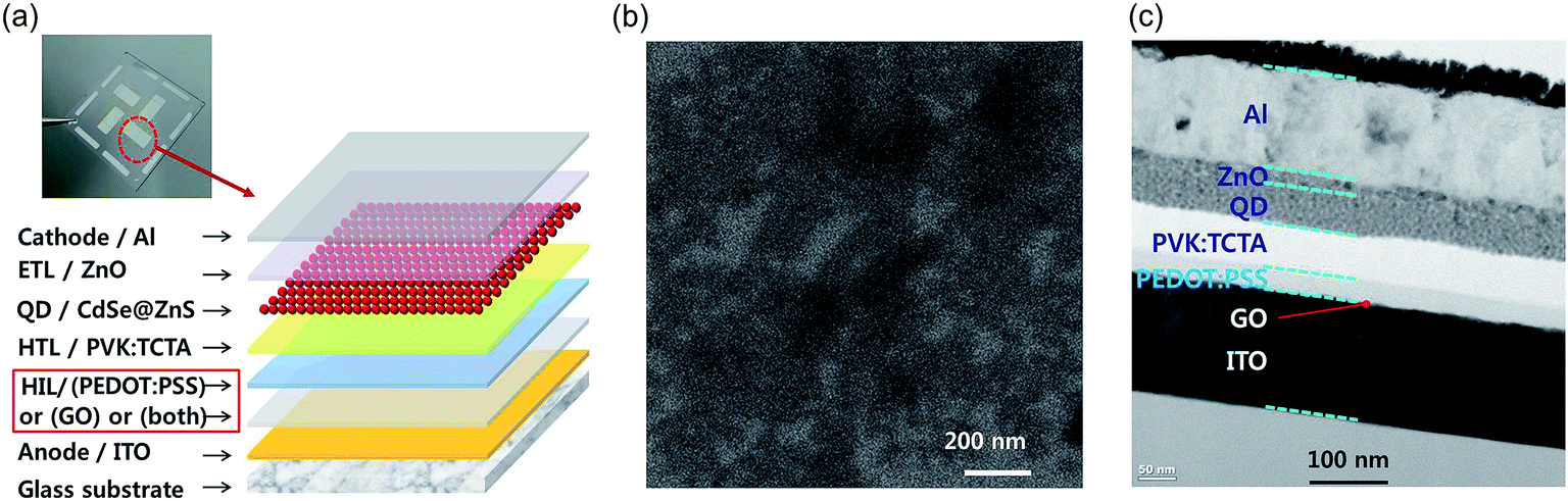 | ||
| Fig. 1 (a) Schematic of QLED device structure and (top) photograph of a device. (b) FESEM image of GO particles on Si wafer. Dark and bright regions correspond to GO-coated and uncoated areas, respectively. (c) Cross-sectional HRTEM image of a QLED device with GO–PEDOT:PSS bilayer HIL. | ||
The composition of CdSe@ZnS QD was analyzed using inductively coupled plasma-mass spectroscopy (ICP-MS) and combustion ion chromatography (CIC) analyses (ESI Fig. S2.†). The compositions of Cd, Se, and Zn were 12.9, 4.75, and 40.9%, respectively, according to ICP-MS analysis, and sulphur was detected in CIC analysis.
The 2 nm-thick GO layer, which was obtained by spin-coating at 5000 rpm, is analyzed using FESEM, as shown in Fig. 1(b). Most of area is covered by GO, but uncoated area is also observed. The cross-sectional image of QLEDs was obtained by high-resolution transmission electron microscopy (HRTEM), JEM-2100F (JEOL, Japan), as shown in Fig. 1(c). The measurements of current, voltage, and electroluminescence characteristics (I–V–L) of the QLEDs were performed using a spectroradiometer, CS-2000 (Konica Minolta, Japan) and an electrometer (Keithley 2400, USA). The photoluminescence (PL) spectra and UV-vis absorption of the QDs were recorded with spectroscopes, FS-2 (SCINCO, Korea) and UV-1800 (Shimadzu, Japan), respectively.
Results and discussion
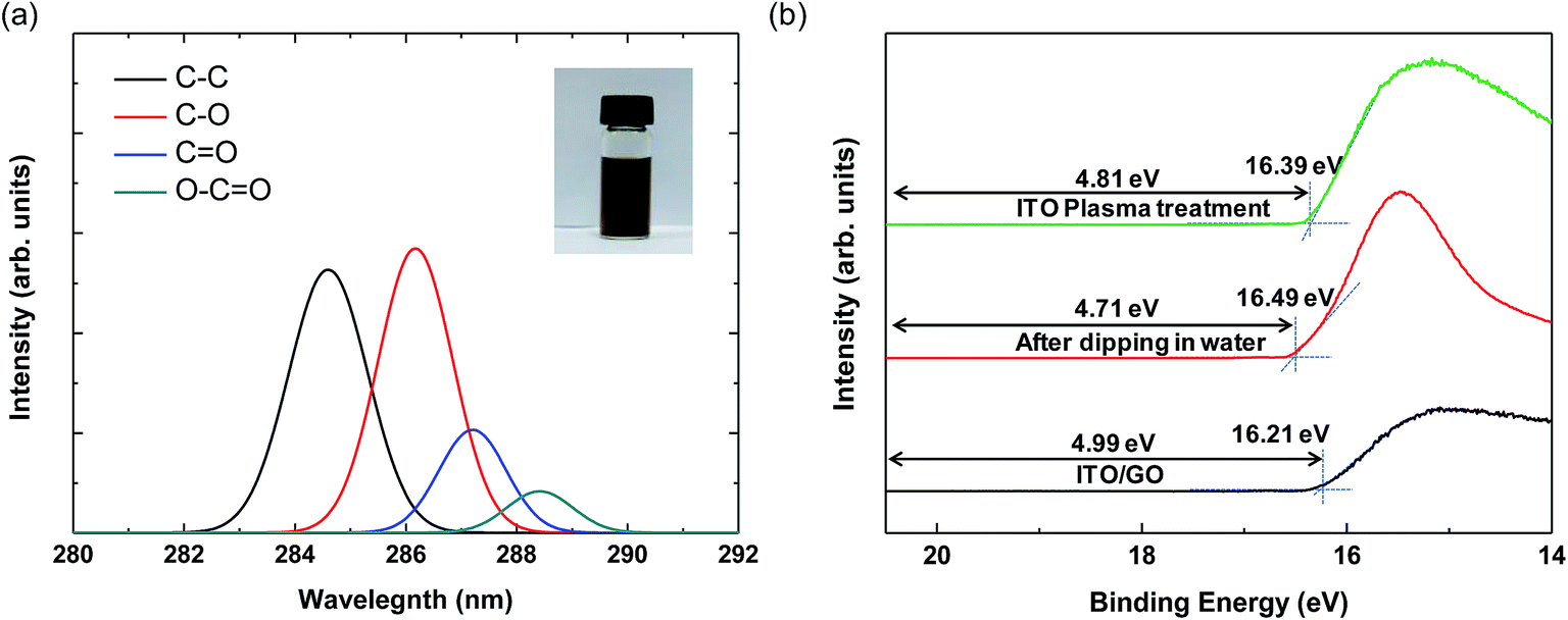
The inset image in Fig. 2(a) shows 0.5 wt% aqueous GO dispersion in a bottle. XPS measurement was performed to analyze the degree of oxidation of the GO particles.28 As shown in Fig. 2(a), the C 1s XPS spectrum of GO has four peaks at approximately 284.6, 286.6, 287.5, and 288.5 eV, which correspond to sp2 carbon (C–C), epoxide (C–O), carbonyl (C![[double bond, length as m-dash]](https://www.rsc.org/images/entities/char_e001.gif) O), and carboxyl (O–CO) functional groups.29 Compared to the intensity of the C–C peak, the peaks for the oxide groups are significantly larger, indicating the good oxidation of GO particles.28 We also measured the zeta potential to confirm the dispersion stability of GO; the value was −58 mV, arising from the negative ionization of the functional groups on the GO basal planes and indicating that the electrostatic repulsion between GO particles is sufficiently large to form a stable colloidal state.30 Thus, the GO dispersion in our experiment is well oxidized and suitable for solution processing.
O), and carboxyl (O–CO) functional groups.29 Compared to the intensity of the C–C peak, the peaks for the oxide groups are significantly larger, indicating the good oxidation of GO particles.28 We also measured the zeta potential to confirm the dispersion stability of GO; the value was −58 mV, arising from the negative ionization of the functional groups on the GO basal planes and indicating that the electrostatic repulsion between GO particles is sufficiently large to form a stable colloidal state.30 Thus, the GO dispersion in our experiment is well oxidized and suitable for solution processing.
 | ||
| Fig. 2 (a) XPS spectra for GO, inset image depicts synthesized GO in DI water. (b) UPS spectra ITO and ITO/GO. | ||
To elucidate the energy band structures for the QLED devices with different HIL layers, we analyzed the work function of a GO layer on an ITO substrate using ultraviolet photoelectron spectroscopy (UPS). Fig. 2(b) shows the UPS spectra of the secondary electron cutoff region for ITO and ITO/GO layers. We calculate the work function (Φ) by subtracting the secondary electron cutoff energy (Ecutoff − EFermi) from the photon energy (hυ) of the UV source (21.2 eV), using the relationship Φ = hυ − |Ecutoff − EFermi|. First, we measured the UPS of the plasma treated ITO layer, the work function of which was 4.81 eV. However, after dipping the substrate in deionized water and drying it, the work function was reduced to 4.71 eV. It is well-known that water or solvent cleaning decreases the work function of ITO layer due to residual contamination on it.31 Since the GO and PEDOT:PSS layers are deposited using solution processes in water-base solvents, the direct contact of water on ITO is inevitable. Hence, the work function of ITO is hardly higher than 4.71 eV in solution processed devices. The work functions of GO layer was 4.98 eV. These results are similar to those reported elsewhere, in which the work function was measured using either UPS or the Kelvin probe method.17,19 The optical band gap of GO is known to be ∼3.6 eV from the Tauc plot using the relation αhυ ∝ (hυ − Eg)1/2, where α and Eg are the absorption coefficient and the optical band gap, respectively.18 The work function of PEDOT:PSS is known to be 5.20 eV.32 Based on the known work functions and band gaps for the other materials used in our QLED devices, the band structures of the QLEDs can be diagrammed as shown in Fig. 3. The energy band diagram clearly shows that the energy difference from the ITO to the HOMO of QDs (1.8 eV) is much larger than that from Al to the LUMO of QDs (0.3 eV). Hence, electron injection is relatively easy and the insertion of ZnO layer is sufficient for electron injection and hole blocking. However, hole injection requires much more complicated HIL and HTL structures. The energy barriers between ITO and PEDOT:PSS and between ITO and GO are 0.49 eV and 0.27 eV, respectively (Fig. 3(a) and (b)), and the insertion of GO between ITO and PEDOT:PSS reduces the interfacial energy barrier by introducing a stepwise energy state.
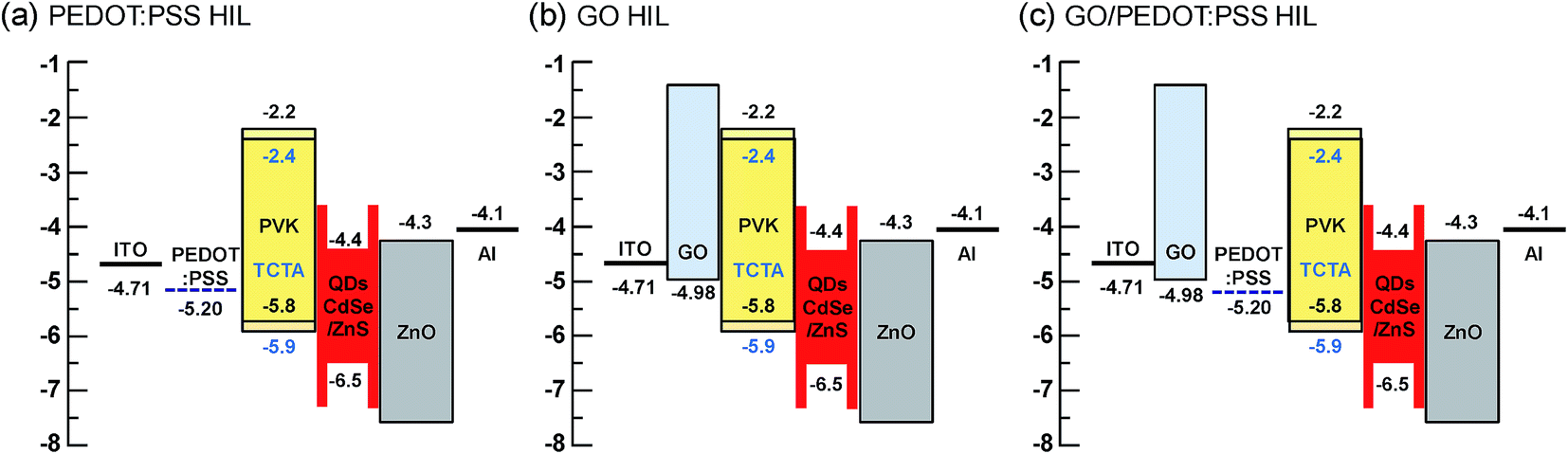 | ||
| Fig. 3 Energy level diagrams of QLEDs using (a) PEDOT:PSS, (b) GO, and (c) GO/PEDOT:PSS for HILs. | ||
In order to optimize the GO layer thickness for HIL, we first fabricated QLED cells with varying thicknesses of GO HIL without using a PEDOT:PSS layer. By controlling the speed of the spin-coater, the thicknesses of the GO layers were tuned to approximately 0, 2, 4, 6, and 10 nm. The current density and luminance of the devices as a function of the applied voltage are shown in Fig. 4. Without GO layer, the luminance performance was poor, and only weak emission was observed at the applied voltage higher than 25 V. Adoption of GO layer dramatically improved the overall performance. It is obvious that GO layer works well as a hole injection layer. As the thickness of the GO layer decreases from 10 nm to 2 nm, both the luminance and the current efficiency significantly increase, and the turn-on voltage decreases from 8.50 V to 5.90 V. Thus, a thinner GO layer is better for HIL functionality. The result may relate to the resistance of GO layer. Although GO has the appropriate work function, it is regarded as an insulating material with highly oxidized sp3 functional groups. Hence, the increasing thickness of the GO layer causes increased resistance and decreased luminance and efficiency.
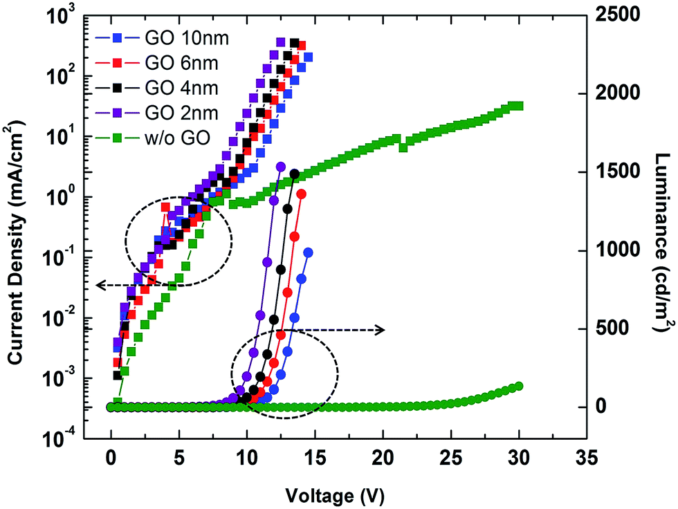 | ||
| Fig. 4 Current density–voltage–luminance characteristics for GO–QLEDs with GO layers of varying thickness. | ||
Then, we fabricated the three types of QLED devices with different HIL layers as illustrated in Fig. 3. The luminance–voltage plots and current density–voltage plots for the three devices are shown in Fig. 5, and the characteristics of luminance, current efficiency, external quantum efficiency, and turn-on voltage of the three QLED devices are summarized in Table 1. First, the comparison between the PEDOT:PSS and GO devices elucidates the effectiveness of the GO layer as HIL compared to that of PEDOT:PSS. The turn-on voltage (Vth), that is, the voltage at 1 cd m−2 of the GO device, is 6.75 V, which is lower than that of the PEDOT:PSS device (8.3 V). This improvement of the turn-on voltage may be attributed to the reduction of the energy barrier from the anode to HIL. However, all other performances of the GO device, including maximum luminance and quantum efficiency, are inferior to those of the PEDOT:PSS device, which may arise from the high resistivity of GO layer.
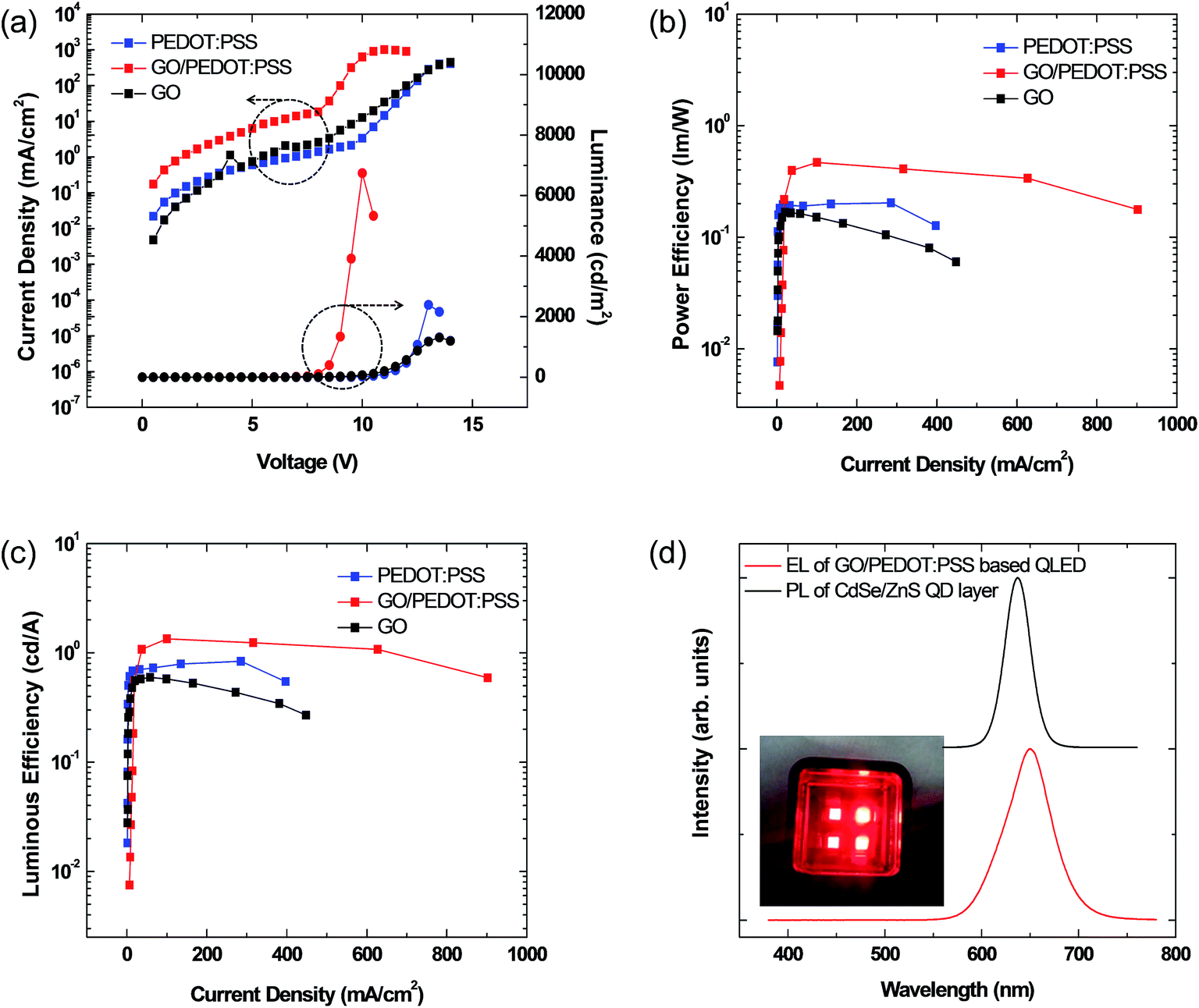 | ||
| Fig. 5 (a) Current density and luminance versus voltage, (b) power efficiency versus current density. (d) Normalized PL spectrum of CdSe/ZnS thin film and EL spectrum of GO/PEDOT:PSS-based QLED and (c) luminous efficiency versus current density characteristics of QLEDs with various HIL structures. The legends indicate the HIL structures. | ||
| Maximum luminance [cd m−2] | C/EMax [cd A−1] | P/EMax [lm W−1] | EQEMax [%] | Vth [V] at 1 cd m−2 | CIE1931 x | CIE1931 y | |
|---|---|---|---|---|---|---|---|
| PEDOT:PSS | 2391 | 0.84 | 0.20 | 1.16 | 8.30 | 0.70 | 0.31 |
| GO | 1309 | 0.60 | 0.17 | 0.77 | 6.75 | 0.70 | 0.31 |
| GO/PEDOT:PSS | 6741 | 1.34 | 0.47 | 1.61 | 5.35 | 0.70 | 0.32 |
Next, we compare the GO/PEDOT:PSS bilayer HIL device to the PEDOT:PSS HIL device. The maximum luminance of the GO/PEDOT:PSS-based QLED is threefold higher (6741 cd m−2) than that of the PEDOT:PSS-based QLED (2391 cd m−2). In addition, the turn-on voltage is dramatically improved from 8.30 V to 5.35 V. Fig. 5(b) and (c) are the plots of the power efficiency–current density and luminance efficiency–current density. The maximum current efficiency is increased from 0.84 cd A−1 to 1.34 cd A−1, and the power efficiency is also increased from 0.20 to 0.47, respectively. Furthermore, the efficiency roll-off also improves using the GO/PEDOT:PSS bilayer HIL. These improvements are attributed to the improved charge balance in the QD layer by the efficient hole injection and transport from ITO to the HTL/QDs facilitated by the introduction of the GO layer.7 These results clearly show that the optimization of the energy band structure near the anode interface is necessary for the optical performance of QLEDs, and that the insertion of a GO layer between ITO and PEDOT:PSS can dramatically improve the hole injection ability.
Fig. 5(d) shows the electroluminescence (EL) spectrum of the GO/PEDOT:PSS-based QLED and the PL spectrum of the CdSe@ZnS core–shell QD thin layer. The maximum emission peaks of the PL and EL spectra are ∼637 and ∼649 nm, respectively. The full width at half-maximum (FWHM) of the PL and EL spectra are ∼31 and ∼58 nm, respectively. The maximum peak difference between the PL and EL spectra is ∼12 nm, caused by either the electric-field-induced Stark effect or the enhanced inter-dot interactions arising from the decreased inter-dot distance in close-packed QDs.33 The PL and EL spectral shapes are almost the same and do not show any side peaks from neighboring organic layers, indicating that the emission of EL from the GO/PEDOT:PSS-based QLED originates from the electron–hole recombination in the CdSe@ZnS core–shell QD layer.
Fig. 6 shows the J–V electrical properties of the QLEDs in double logarithmic plots. The GO/PEDOT:PSS-based QLED shows three conduction regions, similar to the PEDOT:PSS-based QLED. Ohmic conduction (J ∝ V) appears up to 2.0 V, trap-limited conduction (J ∝ Vm, m > 3) dominates up to 14 V, and space charge-limited conduction (J ∝ Vm, m ≈ 2) occurs at higher voltages. The current density of GO/PEDOT:PSS-based device is much higher than that of PEDOT:PSS-based QLED, which also confirms the improved hole injection.1,34 Thus, the incorporation of GO films with the PEDOT:PSS HIL layer is promising in improving the charge balance in QLED devices.
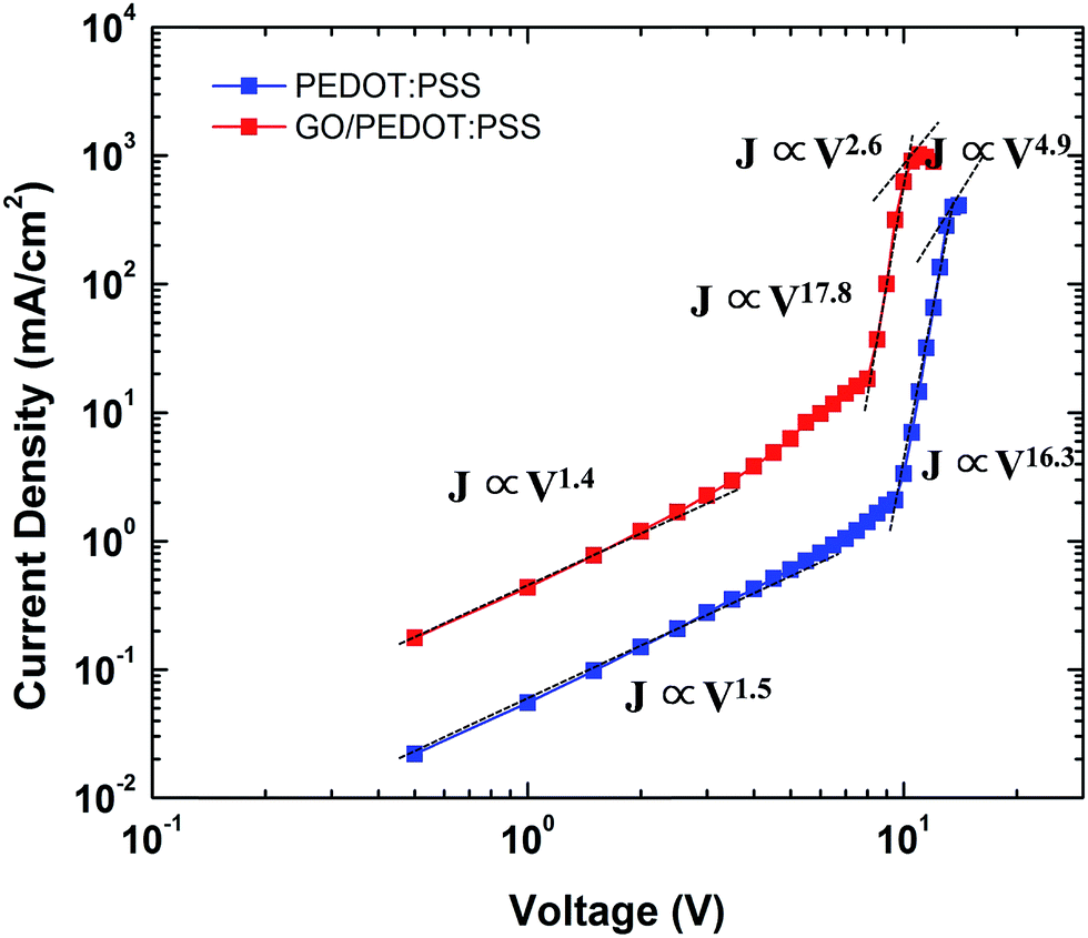 | ||
| Fig. 6 Logarithmic plot of voltage versus current characteristics of QLEDs using PEDOT:PSS and GO/PEDOT:PSS HILs. | ||
Conclusion
In QLED devices, excellent hole injection and transport is necessary to improve the electroluminescent efficiency, because the difference between HOMO level in QDs and the Fermi energy of ITO is significantly large, which is partially enhanced by the solution process of HIL layer on ITO layer. We demonstrated that the use of GO/PEDOT:PSS bilayer as an HIL is effective in improving the hole injection ability. Both GO and PEDOT:PSS are independently good HIL materials; the GO layer has a better turn-on voltage, while PEDOT:PSS is better in quantum efficiency, conductivity, and maximum luminance. The simple combination of GO and PEDOT:PSS induced highly synergistic effects for all electro-optical properties, and the performance of the QLED device with a GO/PEDOT:PSS bilayer HIL exhibited the best properties, including a threefold increase in brightness and external quantum efficiency, twofold increase in current efficiency, and turn-on voltage reduction of 3.2 V. These improvements are attributed to the reduction of the energy barriers between the anode and HTL/QD layers by introducing well-matched stepwise energy levels from the GO/PEDOT:PSS bilayers. It is noteworthy that the adoption of GO/PEDOT:PSS bilayer results in only a slight enhancement of power conversion efficiency in solar cells,17,20 but the same structure brings about dramatic improvement in QLED devices, which clearly shows that the hole injection ability in QLED is highly important.Conflicts of interest
There are no conflicts to declare.Acknowledgements
This work was supported by the National Research Foundation of Korea (NRF) funded by the Ministry of Science and ICT (NRF-2014R1A2A1A11054392 and NRF-2016H1D3A1938043).References
- K.-S. Cho, E. K. Lee, W.-J. Joo, E. Jang, T.-H. Kim, S. J. Lee, S.-J. Kwon, J. Y. Han, B.-K. Kim, B. L. Choi and J. M. Kim, Nat. Photonics, 2009, 3, 341–345 CrossRef CAS.
- S. Coe-Sullivan, Nat. Photonics, 2009, 3, 315–316 CrossRef CAS.
- P. O. Anikeeva, J. E. Halpert, M. G. Bawendi and V. Bulovic, Nano Lett., 2009, 9, 2532–2536 CrossRef CAS PubMed.
- G. J. Supran, Y. Shirasaki, K. W. Song, J.-M. Caruge, P. T. Kazlas, S. Coe-Sullivan, T. L. Andrew, M. G. Bawendi and V. Bulović, MRS Bull., 2013, 38, 703–711 CrossRef.
- V. L. Colvin, M. C. Schlamp and A. P. Alivisatos, Nature, 1994, 370, 354–357 CrossRef CAS.
- J. Kwak, W. K. Bae, D. Lee, I. Park, J. Lim, M. Park, H. Cho, H. Woo, D. Y. Yoon, K. Char, S. Lee and C. Lee, Nano Lett., 2012, 12, 2362–2366 CrossRef CAS PubMed.
- H. M. Kim, J. Kim, J. Lee and J. Jang, ACS Appl. Mater. Interfaces, 2015, 7, 24592–24600 CAS.
- J. Lim, W. K. Bae, J. Kwak, S. Lee, C. Lee and K. Char, Opt. Mater. Express, 2012, 2, 594–628 CrossRef.
- J. Huang, P. F. Miller, J. S. Wilson, A. J. de Mello, J. C. de Mello and D. D. C. Bradley, Adv. Funct. Mater., 2005, 15, 290–296 CrossRef CAS.
- W. K. Bae, Y. S. Park, J. Lim, D. Lee, L. A. Padilha, H. McDaniel, I. Robel, C. Lee, J. M. Pietryga and V. I. Klimov, Nat. Commun., 2013, 4, 2661 Search PubMed.
- H. Shen, W. Cao, N. T. Shewmon, C. Yang, L. S. Li and J. Xue, Nano Lett., 2015, 15, 1211–1216 CrossRef CAS PubMed.
- X. Yang, E. Mutlugun, Y. Zhao, Y. Gao, K. S. Leck, Y. Ma, L. Ke, S. T. Tan, H. V. Demir and X. W. Sun, Small, 2014, 10, 247–252 CrossRef CAS PubMed.
- H. Zhang, S. Wang, X. Sun and S. Chen, J. Mater. Chem. C, 2017, 5, 817–823 RSC.
- T.-H. Han, S.-H. Jeong, Y. Lee, H.-K. Seo, S.-J. Kwon, M.-H. Park and T.-W. Lee, J. Inf. Disp., 2015, 16, 71–84 CrossRef CAS.
- Y.-J. Lin, F.-M. Yang, C.-Y. Huang, W.-Y. Chou, J. Chang and Y.-C. Lien, Appl. Phys. Lett., 2007, 91, 092127 CrossRef.
- F. Chen, Q. Lin, H. Wang, L. Wang, F. Zhang, Z. Du, H. Shen and L. S. Li, Nanoscale Res. Lett., 2016, 11, 376 CrossRef PubMed.
- D. Y. Lee, S. I. Na and S. S. Kim, Nanoscale, 2016, 8, 1513–1522 RSC.
- D.-Y. Wang, I. S. Wang, I. S. Huang, Y.-C. Yeh, S.-S. Li, K.-H. Tu, C.-C. Chen and C.-W. Chen, J. Phys. Chem. C, 2012, 116, 10181–10185 CAS.
- S.-S. Li, K.-H. Tu, C.-C. Lin, C.-W. Chen and M. Chhowalla, ACS Nano, 2010, 4, 3169–3174 CrossRef CAS PubMed.
- Y. Park, K. Soon Choi and S. Young Kim, Phys. Status Solidi A, 2012, 209, 1363–1368 CrossRef CAS.
- S. Rafique, S. M. Abdullah, M. M. Shahid, M. O. Ansari and K. Sulaiman, Sci. Rep., 2017, 7, 39555 CrossRef CAS PubMed.
- W. S. Hummers and R. E. Offema, J. Am. Chem. Soc., 1958, 80, 1339 CrossRef CAS.
- R. T. Ahmad, T. Z. Shen, A. R. Masud, T. K. Ekanayaka, B. Lee and J. K. Song, Langmuir, 2016, 32, 13458–13463 CrossRef CAS PubMed.
- T.-Z. Shen, S.-H. Hong, B. Lee and J.-K. Song, NPG Asia Mater., 2016, 8, e296 CrossRef CAS.
- T.-Z. Shen, S. H. Hong and J. K. Song, Carbon, 2014, 80, 560–564 CrossRef CAS.
- M. Khan, A. H. Al-Marri, M. Khan, N. Mohri, S. F. Adil, A. Al-Warthan, M. R. H. Siddiqui, H. Z. Alkhathlan, R. Berger, W. Tremel and M. N. Tahir, RSC Adv., 2014, 4, 24119–24125 RSC.
- D. Antiohos, G. Folkes, P. Sherrell, S. Ashraf, G. G. Wallace, P. Aitchison, A. T. Harris, J. Chen and A. I. Minett, J. Mater. Chem., 2011, 21, 15987 RSC.
- D. Chen, H. Feng and J. Li, Chem. Rev., 2012, 112, 6027–6053 CrossRef CAS PubMed.
- T.-Z. Shen, S.-H. Hong, J.-K. Guo and J.-K. Song, Carbon, 2016, 105, 8–13 CrossRef CAS.
- D. Li, M. B. Muller, S. Gilje, R. B. Kaner and G. G. Wallace, Nat. Nanotechnol., 2008, 3, 101–105 CrossRef CAS PubMed.
- K. Sugiyama, H. Ishii, Y. Ouchi and K. Seki, J. Appl. Phys., 2000, 87, 295–298 CrossRef CAS.
- J. A. Mikroyannidis, A. N. Kabanakis, D. V. Tsagkournos, P. Balraju and G. D. Sharma, J. Mater. Chem., 2010, 20, 6464 RSC.
- H. H. Kim, S. Park, Y. Yi, D. I. Son, C. Park, D. K. Hwang and W. K. Choi, Sci. Rep., 2015, 5, 8968 CrossRef CAS PubMed.
- T.-H. Kim, K.-S. Cho, E. K. Lee, S. J. Lee, J. Chae, J. W. Kim, D. H. Kim, J.-Y. Kwon, G. Amaratunga, S. Y. Lee, B. L. Choi, Y. Kuk, J. M. Kim and K. Kim, Nat. Photonics, 2011, 5, 176–182 CrossRef CAS.
Footnote |
| † Electronic supplementary information (ESI) available. See DOI: 10.1039/c7ra07948f |
| This journal is © The Royal Society of Chemistry 2017 |