
 Open Access Article
 This Open Access Article is licensed under a
 Creative Commons Attribution 3.0 Unported Licence
Large-area electrospray-deposited nanocrystalline CuXO hole transport layer for perovskite solar cells†
Ian Y. Y. Bu a,
Yaw-Shyan Fu*a,
Jian-Fu Lia and
Tzung-Fang Guobc
a,
Yaw-Shyan Fu*a,
Jian-Fu Lia and
Tzung-Fang Guobc
aDepartment of Greenergy, National University of Tainan, Taiwan. E-mail: ysfu@mail.nutn.edu.tw
bDepartment of Photonics, National Cheng Kung University, Tainan, Taiwan
cAdvanced Optoelectronic Technology Center, National Cheng Kung University, Tainan, Taiwan
First published on 3rd October 2017
Abstract
Spin-coating deposition is widely employed for the fabrication of perovskite solar cells (PSCs) due to its conformal coating ability and simple set-up. Although spin-coating deposition is a proven technique for obtaining high-performance PSCs, it is a single-substrate process with low throughput and is therefore unsuitable for commercial PSC production. Herein, we report an industrial-production-compatible electrospray deposition process for the preparation of the hole transport layer (HTL) and active layer in PSCs. Using electrosprayed CuXO as the HTL, we fabricated a solar cell with a power conversion efficiency of 5.83%, a short-circuit current density of 17.22 mA cm2, an open circuit voltage of 0.7 V, and a fill factor of 0.48. This device outperforms PSCs (with identical device structure) fabricated using a PEDOT:PSS film (efficiency: 4.01%).
Introduction
Organic–inorganic hybrid metal halide perovskite solar cells (PSCs) have attracted significant research attention due to their high power conversion efficiency (PCE) and potentially low-cost fabrication process.1,2 The PCE of PSCs (22.1%)3 has overtaken that of other emerging solar cell technologies and is rapidly approaching that of crystalline-silicon-based solar cells, the current market-leading technology. A perovskite crystal layer is well-suited to serve as the active layer in photovoltaic devices due to its high absorption coefficient and long diffusion length.4Generally, PSCs have either a mesoporous5 or a planar heterojunction configuration.1 In the mesoporous heterojunction configuration, a metal-oxide-nanoparticle scaffold is used to support the perovskite absorber layer. This requires a high-temperature sintering process and has been identified as one of the main causes of hysteresis in current–voltage characteristics.6,7 These issues can be suppressed by adopting the planar heterojunction configuration in inverted mode, with the perovskite layer sandwiched between a hole transport layer (HTL) and an electron transport layer (ETL).8,9
Poly(3,4-ethylene dioxythiophene):poly(styrene sulfonate) (PEDOT:PSS) is commonly used as the HTL in planar heterojunction PSCs due to its consistent performance and conformity.10,11 However, PEDOT:PSS has two drawbacks; it is expensive and thus unsuitable for commercial PSC production, and its acidity has been shown to etch the underlying indium tin oxide (ITO) layer and degrade the perovskite layer.12,13 Consequently, metal-oxide-based HTL materials, such as NiO14,15 and GeO,16 have been proposed as alternatives to PEDOT:PSS. Devices with metal oxide HTLs have demonstrated photovoltaic performance similar to that of devices fabricated using PEDOT:PSS but with enhanced stability.
Copper oxide CuXO, a naturally p-type semiconductor, has been extensively studied due to its potential application in sensors, superconductors, and absorber layers in solar cells. Copper oxides have been employed as the HTL in PSCs; they form an ohmic contact between the anode and the perovskite layer. Zuo17 first integrated Cu2O and CuO into PSCs by using a spin-coating process. Although a high PCE was obtained, the process relies on an organic PEDOT:PSS buffer layer between the CuO layer and the ITO substrate. Nejand18 and Yu19 completely removed the PEDOT:PSS layer from the PSC device, using only a sputtered Cu2O layer as the HTL in a PSC; they obtained PCE values of 8.93% and 11%, respectively. Sun20 used a solution-processed CuOx HTL and obtained a PCE of ∼17%. Although high PCE values have been obtained with CuOx as the HTL, the proposed methods are difficult to integrate into large-area industrial production of PSCs since the perovskite layers are still deposited using the spin-coating process and are highly sensitive to moisture.
Most reported perovskite photovoltaic devices have been fabricated using a precursor solution. Usually, the perovskite layer is prepared via the annealing of a spin-coated solution or the coating of pre-synthesized perovskite nanocrystals. A spin-coated perovskite layer usually consists of a matrix of nanocrystalline grains. Although spin-coating deposition offers a simple set-up and uniform coating, it is essentially a single-substrate process and thus offers limited throughput, making it unsuitable for commercial PSC production. In order to scale up the production of PSCs, an alternative large-area deposition method is needed.
To address the industrial production roadblocks, Barrows21 and Liang22 proposed simple ultrasonic spray deposition of perovskite films on PEDOT:PSS-coated ITO substrates and perovskite film on TiO2-coated fluorine-doped tin oxide (FTO) substrates, respectively. Although the ultrasonic spray process offers a simple set-up and large-area deposition, the technique lacks control and can lead to impurity incorporation and defect formation. Chandrasekhar23 reported the electrospray-assisted deposition of perovskite on TiO2-coated FTO substrates. This deposition process improved the crystallinity, morphology, and coverage of perovskite film. However, all these spray/electrospray deposition processes rely on the spin-coating process for HTL/ETL deposition, which is an obstacle for the full-scale production of PSCs.
To address this issue, we deposited a perovskite layer and an inorganic HTL (CuXO) on an ITO-coated glass substrate using electrostatic spray deposition to form a PSC. Herein, we report a fully scalable and cost-effective approach for fabricating PSCs using the combination of direct electrostatic spray deposition and thermal evaporation on conductive substrates. We optimized the thickness of the perovskite layer by carefully monitoring the deposition time and fabricated a PSC device using the proposed process.
Experiments
Copper acetate (99.9%), ethanolamine (99%), PEDOT:PSS (1.3–1.7 wt%), PbCl2 (99.9%), C60 (99.9%), and bathocuproine (BCP, 99.9%) were purchased from Sigma Aldrich and used without further purification. 0.7 cm-thick ITO-coated glass substrates (sheet resistance: 10 Ω) with ≥84% optical transparency were purchased from GemTech Optoelectronics (Taiwan). Perovskite methylammonium iodide (CH3NH3I) precursor solution was synthesized by dissolving 9.74 wt% CH3NH3I and PbCl2 (3![[thin space (1/6-em)]](https://www.rsc.org/images/entities/char_2009.gif) :1) into dimethylformamide (DMF). The CuXO precursor solutions were prepared by mixing 1.5 × 10⁻² M copper acetate in isopropanol solution with the pH of the precursor solution adjusted to 11 with ammonia.
:1) into dimethylformamide (DMF). The CuXO precursor solutions were prepared by mixing 1.5 × 10⁻² M copper acetate in isopropanol solution with the pH of the precursor solution adjusted to 11 with ammonia.
Device fabrication
The ITO-coated glass substrates were cleaned by sequential ultrasonication in acetone, isopropanol, and deionized water for 30 min followed by 30 min of ultraviolet-ozone treatment. The electrospray deposition process was performed using a previously reported set-up. For the HTL deposition, a layer of CuXO precursor with various thicknesses was electrosprayed onto a pre-cleaned ITO glass substrate (DC voltage: 8 kV; constant rate: 0.5 mL h−1; velocity of flow deposition time: 10–1800 s) under ambient conditions and post-annealed at 500 °C in air. Similarly, the perovskite layers were electrosprayed with a flow rate of 18 μL min−1 and a DC bias of 20 kV. The electrosprayed mixed halide perovskite precursors were annealing at 110 °C in air. The samples were then transferred to an evaporator to deposit C60 (30 nm) (>99.5%) and BCP (10 nm). Al electrodes (100 nm) were thermally deposited on the substrate inside a vacuum chamber (10−6 Torr). The active area of the device was 0.06 cm2. For comparison, PEDOT:PSS film, to serve as the HTL, was spin-coated onto ITO at 4000 rpm for 60 s and heated at 150 °C for 15 min. As a demonstration a 9 cm2 photovoltaic device were fabricated without Al electrode coating (ESI S.1†). The Al electrode coating would fully cover the underlying layers and shown only metallic surface.Characterization
The morphology of the deposited samples were evaluated by a Zeiss Auriga Ultra-high resolution scanning electron microscope. X-ray diffraction (XRD) patterns of CuXO and perovskite/CuXO were obtained (Bruker D8 Advance ECO, Germany) using a Cu Kα (λ = 0.15418 nm) radiation source operated at 40 kV and 25 mA. The XRD patterns were obtained at a scan rate of 0.05° s−1 in the 2θ range of 20° to 70°. The surface morphology of the CuXO and perovskite films was examined using scanning electron microscopy (SEM, ZEISS AURIGA 39-50).The elemental composition depth profile of CuXO was determined using Auger electron spectroscopy (AES, MICROLAB 350). PSC current density–voltage (J–V) curves were measured in a humidity-controlled, nitrogen-filled glove box using a Keithley 2400 sourcemeter, cells were illuminated using standard 1-sun AM 1.5 simulated solar irradiation (100 mW cm−2) from an Newport 91160A 300 W Solar Simulator (Class A). Time-resolved photoluminescence (TR-PL) spectra were recorded using the time correlated single-photon counting (TCSPC) technique (UniRAM, Protrustech 405 nm excitation) with a 200 ps pulse duration and repetition rate of 20 MHz. XPS measurements were obtained using a Thermo Fisher Scientific Theta Probe with X-ray source using Al Kα = 1486.6 eV.
Results and discussion
AES (Fig. 1(a)) was used to determine the chemical composition and thickness of the deposited CuXO film. Fig. 1(b) shows the thickness of the CuXO film prepared using various deposition times. The AES analysis confirms the presence of Cu and O, with highly Cu-rich Cu2.14O film deposited in the initial 20 nm of the film and film composition shifting toward Cu1.36O with increasing deposition time. The inhomogeneous composition is likely due to the diffusion of oxygen during the annealing process. XPS analysis was used to gain further understanding of the chemical bonding of the CuXO sample. Fig. 1(c) shows distinctive peaks at binding energy of 530.60 eV and 531.25 can be attributed to the oxygen state in CuO and Cu2O, respectively,24–26 confirming the mixed-phase of CuO. | ||
| Fig. 1 (a) Copper and oxygen concentration versus depth profiles in CuXO samples (b) the CuXO thickness as a function of time and (c) XPS analysis of as-deposited CuXO. | ||
The morphology of pristine ITO, ITO/PEDOT:PSS, and ITO/CuXO samples was examined using SEM (Fig. 2). Fig. 2(a) and (b) show SEM images of pristine ITO-coated glass and PEDOT:PSS, respectively. The pristine ITO glass has a clean surface with micron-sized ITO crystals. The PEDOT:PSS-coated ITO/glass is smooth and without pinholes. SEM images of electrosprayed CuXO films deposited for 10 (thickness: 26 nm), 30 (48 nm), 60 (101 nm), and 300 s (181 nm) are shown in Fig. 2(c)–(f), respectively. As shown in Fig. 2(c), the CuXO film deposited for 10 s only partially covered the substrate due to insufficient precursor deposition, with the underlying ITO clearly exposed. Complete coverage of the ITO/glass substrate is critical for obtaining high-performance solar cells, as it prevents a short circuit between the CuXO layer and the ITO layer. Here, complete coverage of the ITO/glass substrate was achieved with a deposition time of 30 s or more (Fig. 2(d)–(f)), with the voids filled by CuXO nanocrystals. Closer examination of the SEM images reveals that CuXO films deposited for a long period (300 s) were thick and had increased agglomeration and surface roughness, which is undesirable for high-performance solar cells. Cross section SEM image (Fig. 2(g)) was taken, with a thin layer of CuXO (∼50 nm) sandwiched between perovskite (317 nm) and ITO (70 nm).
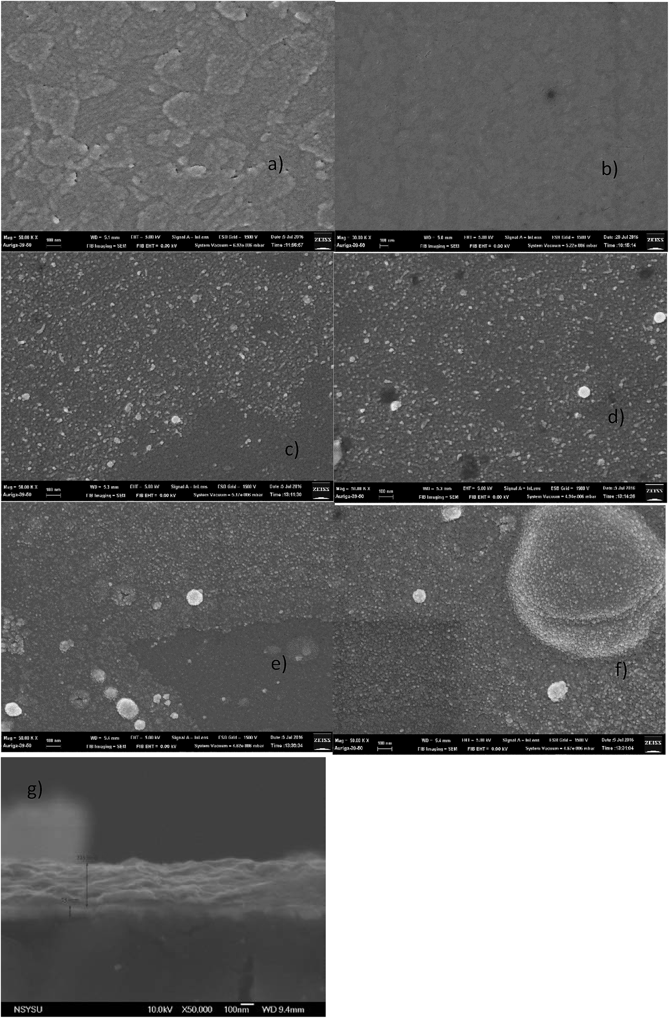 | ||
| Fig. 2 SEM image of (a) ITO, (b) ITO/PEDOT:PSS, (c) ITO/CuOx 26 nm, (d) ITO/CuXO 48 nm, (e) ITO/CuXO 101, (f) ITO/CuXO 181 nm and (g) glass/ITO/CuXO/perovskite (scale bar 100 nm). | ||
The XRD pattern of the CuXO thin film is shown in Fig. 3(a). All reflections can be indexed to the monoclinic CuO phase, with lattice constants comparable to the reported data (JCPDS card no. 89-5899). In Fig. 3(a), the peaks at 2θ values of 35.56°, 38.76°, 48.70° and 61.56° can be indexed to the (002), (111), (202) and (113) phase of CuO, respectively. In addition, Cu2O peaks belonging to (110) and (112) phase can be observed. The mixed phase composition (CuO and Cu2O) is consistent with the AES data. XRD analysis of CH3NH3PbI3−xClx grown on CuXO and PEDOT:PSS was also conducted to determine the effect of the perovskite layer on CuXO deposition (Fig. 3(b)). For the perovskite film deposited on thinner (<180 nm) CuXO, the XRD peaks at (110) and (220), which are attributed to the pure CH3–NH3PbI3−xClx perovskite phase, show that a complete reaction occurred between CH3NH3I and PbCl2. However, for thicker CuXO samples, peaks at 12.6° belonging to (001) phase of PbI2 and 15.1° belonging to (110) phase of CH3NH3PBI3 appear in the XRD pattern, which is an indication of unreacted precursors or the decomposition of CH3NH3PbI3. The appearance of reaction intermediates is due to the formation of agglomerates and cracks on the CuXO surface, which may have been covered by chemisorbed oxygen species such as hydroxide on the surface decompose the perovskite crystal.
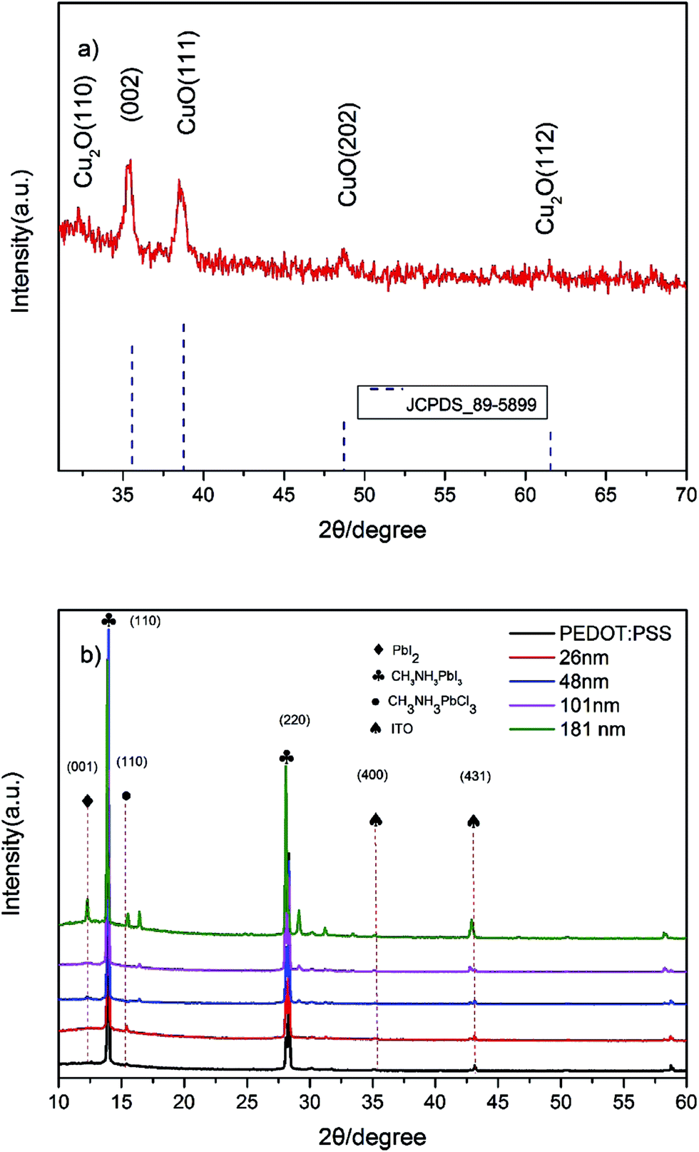 | ||
| Fig. 3 XRD pattern of (a) CuXO film and (b) perovskite deposition and PEDOT:PSS on CuXO layer of various thickness. | ||
CH3NH3PbI3−xClx perovskite-based solar cells were fabricated using CuXO as the HTL. For comparison, a PSC device was fabricated using PEDOT:PSS as the HTL. Fig. 4(a) and (b) show the schematic structure of the fabricated device and the energy level diagram of the device,17,20 with the energy levels obtained from other studies, respectively. The current density–voltage (J–V) characteristics of the fabricated PSCs with various CuXO layers and a reference PEDOT:PSS layer are plotted in Fig. 4(c). The measured device performances were extracted from the J–V curves and are summarized in Table 1.
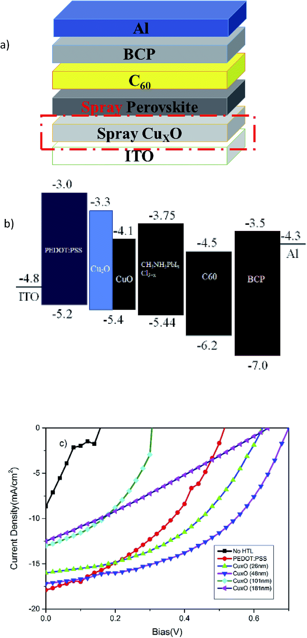 | ||
| Fig. 4 (a) Schematic illustration of the proposed device structure, (b) energy level and (c) J–V characteristics of the fabricated devices. | ||
| Voc (V) | Jsc (mA cm−2) | Fill factor | η (%) | |
|---|---|---|---|---|
| NO HTL | 0.28 | 5.87 | 0.30 | 0.50 |
| PEDOT:PSS | 0.58 | 17.14 | 0.40 | 4.01 |
| CuXO 26 nm | 0.63 | 16.03 | 0.46 | 4.59 |
| CuXO 48 nm | 0.70 | 17.22 | 0.48 | 5.83 |
| CuXO 101 nm | 0.64 | 10.80 | 0.41 | 2.87 |
| CuXO 181 nm | 0.33 | 11.47 | 0.44 | 1.67 |
'The reference device has a short-circuit current density (Jsc) of 17.14 mA cm−2, an open-circuit voltage (Voc) of 0.58 V, a fill factor (FF) of 0.40, and a PCE of 4.01%. For the CuXO-based PSCs, the thickness of the CuXO layer significantly influences solar cell performance. PSCs fabricated using 26 nm-thick CuO have a Voc of 0.63 V, an FF of 0.46, a Jsc of 16.03 mA cm−2, and an overall PCE of ∼4.59%. When the CuO thickness was increased to 48 nm, the PCE increased to 5.83%, with improvement in all key solar cell parameters (Voc: 0.70 V; FF: 0.48; Jsc: 17.22 mA cm−2). Table 1 also reveals that a further increase in CuXO thickness resulted in degradation in solar cell performance. The comparatively inferior solar cell performance for the thinner CuXO (26 nm) is due to incomplete coverage of the HTL, which can lead to increased leakage current and degradation in performance. When CuXO thickness was increased to 48 nm, the performance improved due to better surface coverage. When the CuXO thickness was increased to beyond 48 nm, the combination of increased series resistance and light absorption from using a thicker CuXO HTL degraded performance. The results show that there exists an optimal CuXO thickness for the efficient PSCs·CuXO.
In order to evaluate the quality of the HTL, steady-state photoluminescence (PL) and time-resolved PL decay were measured for MAPbI3 films on PEDOT:PSS-coated ITO and CuXO-coated ITO substrates (as a function of deposition time). Fig. 5(a) shows PL quenching of the samples. Stronger PL quenching can be observed for the optimized CuXO HTL compared to that for PEDOT:PSS, confirming the hole-extraction capability of CuXO. The time-resolved PL decay measured at the peak emission at 765 nm is shown in Fig. 5(b). The PL times of the CuXO/perovskite and PEDOT:PSS samples were fitted with a double exponential decay function, which includes fast and slow decay processes. The fast decay is usually attributed to the bimolecular recombination between the perovskite layer and the HTL, and the slow decay originates from free carrier recombination. The bare perovskite film exhibits an average decay time of 10.9 ns; this decreased to 6.5 and 3.3 ns when the perovskite layer was coated with PEDOT:PSS and CuXO, respectively. This indicates that improved hole extraction and charge dissociation were achieved at the CuXO/MAPbI3 interface. These results demonstrate that CuXO can be used as a replacement for PEDOT:PSS as the HTL in high-performance PSCs.
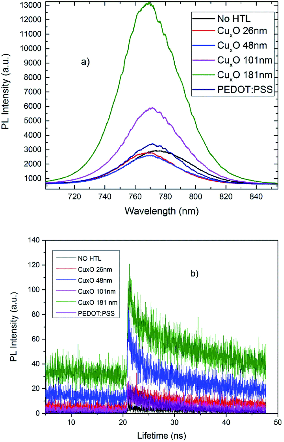 | ||
| Fig. 5 (a) PL emission spectra of CuXO (excitation wavelength of the PL measurements was 600 nm) (b) time-resolved PL measurements taken at the peak emission wavelength (765 nm) of the various HTLs. | ||
Conclusion
This study demonstrated a method suitable for large-area industrial production of PSCs using a combination of electrospray deposition and thermal evaporation. It was found that the thickness of the electrospray-deposited CuOx layer significantly influences PSC performance. An insufficient CuOx thickness leads to poor solar cell performance due to poor surface coverage, whereas an excessively thick CuO HTL degrades solar cell performance due to increased light absorption and series resistance. The optimized PSC exhibited a PCE of 5.83%, a Jsc of 17.22 mA cm−2, a Voc of 0.7 V, and an FF of 0.48. This PSC outperforms PSCs (with identical device structure) fabricated using state-of-the-art polymers (PEDOT:PSS) (PCE: 4.01%).Conflicts of interest
There are no conflicts to declare.References
- M. Liu, M. B. Johnston and H. J. Snaith, Nature, 2013, 501, 395–398 CrossRef CAS PubMed.
- J. You, L. Meng, T.-B. Song, T.-F. Guo, Y. M. Yang, W.-H. Chang, Z. Hong, H. Chen, H. Zhou and Q. Chen, Nat. Nanotechnol., 2015, 75 CrossRef PubMed.
- http://www.nrel.gov/ncpv/images/efficiency_chart.jpg.
- S. D. Stranks, G. E. Eperon, G. Grancini, C. Menelaou, M. J. Alcocer, T. Leijtens, L. M. Herz, A. Petrozza and H. J. Snaith, Science, 2013, 342, 341–344 CrossRef CAS PubMed.
- A. Mei, X. Li, L. Liu, Z. Ku, T. Liu, Y. Rong, M. Xu, M. Hu, J. Chen and Y. Yang, Science, 2014, 345, 295–298 CrossRef CAS PubMed.
- H.-S. Kim and N.-G. Park, J. Phys. Chem. Lett., 2014, 5, 2927–2934 CrossRef CAS PubMed.
- H. J. Snaith, A. Abate, J. M. Ball, G. E. Eperon, T. Leijtens, N. K. Noel, S. D. Stranks, J. T.-W. Wang, K. Wojciechowski and W. Zhang, J. Phys. Chem. Lett., 2014, 5, 1511–1515 CrossRef CAS PubMed.
- J. H. Heo, H. J. Han, D. Kim, T. K. Ahn and S. H. Im, Energy Environ. Sci., 2015, 8, 1602–1608 CAS.
- C.-G. Wu, C.-H. Chiang, Z.-L. Tseng, M. K. Nazeeruddin, A. Hagfeldt and M. Grätzel, Energy Environ. Sci., 2015, 8, 2725–2733 CAS.
- O. Malinkiewicz, A. Yella, Y. H. Lee, G. M. Espallargas, M. Graetzel, M. K. Nazeeruddin and H. J. Bolink, Nat. Photonics, 2014, 8, 128–132 CrossRef CAS.
- P. Docampo, J. M. Ball, M. Darwich, G. E. Eperon and H. J. Snaith, Nat. Commun., 2013, 4, 2761 Search PubMed.
- J. M. Yun, J. S. Yeo, J. Kim, H. G. Jeong, D. Y. Kim, Y. J. Noh, S. S. Kim, B. C. Ku and S. I. Na, Adv. Mater., 2011, 23, 4923–4928 CrossRef CAS PubMed.
- Z. Zhu, Y. Bai, T. Zhang, Z. Liu, X. Long, Z. Wei, Z. Wang, L. Zhang, J. Wang and F. Yan, Angew. Chem., 2014, 126, 12779–12783 CrossRef.
- J. Y. Jeng, K. C. Chen, T. Y. Chiang, P. Y. Lin, T. D. Tsai, Y. C. Chang, T. F. Guo, P. Chen, T. C. Wen and Y. J. Hsu, Adv. Mater., 2014, 26, 4107–4113 CrossRef CAS PubMed.
- J. H. Park, J. Seo, S. Park, S. S. Shin, Y. C. Kim, N. J. Jeon, H. W. Shin, T. K. Ahn, J. H. Noh and S. C. Yoon, Adv. Mater., 2015, 27, 4013–4019 CrossRef CAS PubMed.
- Z.-K. Wang, M. Li, D.-X. Yuan, X.-B. Shi, H. Ma and L.-S. Liao, ACS Appl. Mater. Interfaces, 2015, 7, 9645–9651 CAS.
- C. Zuo and L. Ding, Small, 2015, 11, 5528–5532 CrossRef CAS PubMed.
- B. A. Nejand, V. Ahmadi, S. Gharibzadeh and H. R. Shahverdi, ChemSusChem, 2016, 302–313 CrossRef CAS PubMed.
- W. Yu, F. Li, H. Wang, E. Alarousu, Y. Chen, B. Lin, L. Wang, M. N. Hedhili, Y. Li and K. Wu, Nanoscale, 2016, 8, 6173–6179 RSC.
- W. Sun, Y. Li, S. Ye, H. Rao, W. Yan, H. Peng, Y. Li, Z. Liu, S. Wang and Z. Chen, Nanoscale, 2016, 8, 10806–10813 RSC.
- A. T. Barrows, A. J. Pearson, C. K. Kwak, A. D. Dunbar, A. R. Buckley and D. G. Lidzey, Energy Environ. Sci., 2014, 7, 2944–2950 CAS.
- Z. Liang, S. Zhang, X. Xu, N. Wang, J. Wang, X. Wang, Z. Bi, G. Xu, N. Yuan and J. Ding, RSC Adv., 2015, 5, 60562–60569 RSC.
- P. Chandrasekhar, N. Kumar, S. K. Swami, V. Dutta and V. K. Komarala, Nanoscale, 2016, 8, 6792–6800 RSC.
- H. Liu, Y. Wang, G. Liu, Y. Ren, N. Zhang, G. Wang and T. Li, Acta Metall. Sin. (Engl. Lett.), 2014, 27, 149–155 CrossRef CAS.
- Z. Xu, Y. Yu, D. Fang, J. Liang and L. Zhou, Mater. Chem. Phys., 2016, 171, 386–393 CrossRef CAS.
- I. Y. Bu and R. Huang, Ceram. Int., 2017, 43, 45–50 CrossRef CAS.
Footnote |
| † Electronic supplementary information (ESI) available. See DOI: 10.1039/c7ra07725d |
| This journal is © The Royal Society of Chemistry 2017 |