
 Open Access Article
 This Open Access Article is licensed under a
 Creative Commons Attribution 3.0 Unported Licence
Porous NiO–WO3 heterojunction nanofibers fabricated by electrospinning with enhanced gas sensing properties
Jinniu Zhang ,
Hongbing Lu*,
Chang Liu,
Chujun Chen and
Xia Xin
,
Hongbing Lu*,
Chang Liu,
Chujun Chen and
Xia Xin
School of Physics and Information Technology, Shaanxi Normal University, Xi'an 710062, China. E-mail: hblu@snnu.edu.cn
First published on 18th August 2017
Abstract
A series of NiO–WO3 composite nanofibers with different molar ratios (Ni/W = 0%, 1%, 3% and 5%) were fabricated based on an electrospinning and calcination technique. The gas sensing performances of sensors based on the as-produced nanofibers were studied towards acetone in detail. Compared with the pure WO3 nanofibers, the porous NiO–WO3 composite nanofibers exhibited higher sensitivity, faster response, and shorter recovery time towards acetone. Particularly, the 3 mol% NiO–WO3 heterojunction nanofibers demonstrated the largest sensitivity, exhibiting a prominent value of 22.5 under 100 ppm acetone at the operating temperature of 375 °C, which is almost 2.1 times larger than that of the pure WO3 nanofibers. Moreover, the 3 mol% NiO–WO3 heterojunction nanofibers also exhibited excellent selectivity and long-term stability to acetone. The combined effects including the formation of p–n heterojunctions between NiO and WO3, high oxygen species absorbing capacity, and special porous structural features with high surface area and small grain size, contributed to the enhanced sensing properties of the 3 mol% NiO–WO3 composite nanofibers. These attractive gas sensing properties enable the NiO–WO3 heterojunction nanofibers to be a promising material for application in gas sensors.
1. Introduction
Gas sensors, based on nanomaterials, continue to receive much attention due to a variety of applications in environmental air-quality control, health care, toxic gas detection, and medicine diagnosis.1–4 Many nanomaterials have been widely used for gas sensors, such as TiO2,5,6 SnO2,7–10 ZnO,11–13 WO3,14,15 graphene–Ag,16,17 and carbon nanotubes.18 Among these materials, WO3, an n-type semiconductor material with a band gap of 2.5–3.0 eV, is considered to be a prospective sensor material because of its low cost, facile preparation and excellent electronic properties. Many previous studies of WO3 sensors have paid attention to detecting gases of NO2, H2S, H2 and NH3,19–21 and a few studies also explored the gas sensing properties towards volatile organic compounds (VOCs), such as, methanol, ethanol, n-butanol, and acetone.22–24 Acetone is an important solvent for material synthesis, but it can bring about damage to the central nervous system, eyes and noses at high concentrations (≥173 ppm).25 Although gas sensors have already been reported for the detection acetone based on pristine WO3 nanostructures, such as porous architectures,26 nanocrystals,27 nanotubes,28 nanofibers,29 inverse opal,30 shells,31 and nanosheets,32 further studies on WO3-based sensors are still needed.For the purpose of improving the gas sensing performances of WO3, several approaches have been developed in recent years. The first is the construction of WO3 nanostructures with special morphologies by a variety of methods, such as vacuum deposition,33 spin-coating,34 sputtering,35 and electrospinning.14,15 Compared with other methods, electrospinning is an inexpensive and versatile technique for the fabrication of ultra-long one dimensional (1D) organic or inorganic nanofibers with diameters ranging from the nano to the micrometer scale.36 As we all know, the 1D functional nanomaterials have many good characteristics, such as high surface-to-volume ratio and outstanding carrier transport performance. The second approach is the surface modification of WO3 by noble metals, such as Au/Pt14 and Pd.15 However, morphology-induced improvement of gas sensor performances is still limited, and the high cost also hinders the practical application potential of noble metal modified WO3.
Thirdly, formation of WO3-based composite nanomaterials by adding other metal oxides is a popular strategy to improve gas sensor performances.22–24 Among the various oxide additives, NiO is a p-type semiconductor with an energy gap of 3.5–4.2 eV.37 Importantly, compared with other metal oxides, NiO has obviously higher oxygen species absorbing ability,38 which is very useful for improving gas sensing performance. Gas sensors based on pure NiO nanostructures, such as NiO nanoparticles,39 polycrystalline nanowires,40 and nanoflowers,41 have been demonstrated. Furthermore, NiO can form useful heterojunctions with n-type semiconductors, including SnO2 (ref. 7–9) and WO3,42,43 to further modulate the width of depletion layer. NiO p-type catalysts were employed to enhance the sensing performances of SnO2 towards VOCs, and the results showed that enhanced sensing performances including higher response and selectivity, shorter response–recovery time were obtained through the NiO additive.7–9 Nevertheless, only several articles on NiO–WO3 composite sensing nanomaterials have been reported up to now.42,43 Bao et al.42 synthesized the plate-like heterogeneous NiO–WO3 nanocomposites by the annealing method. Their results showed that the p–n heterogeneous nanocomposites provided the benefits of fast response, improved sensitivity and outstanding selectivity towards NO2 at room temperature. Noh et al.43 prepared the NiO–WO3 composite thick films by the screen-printing technique, and showed that the sensitivity for NO2 increased distinctly for the composite samples with 1.0 mol% NiO.
In this paper, for further improving the sensing performances of WO3 nanostructures, an electrospinning and calcination method was used to fabricate 1D p–n heterogeneous NiO–WO3 composite nanofibers with porous structure. The gas sensing behaviors of the sensors fabricated by the as-prepared WO3 and NiO–WO3 heterojunction nanofibers were systematically explored. The NiO–WO3 heterojunction nanofibers were demonstrated to have markedly higher acetone sensing characteristics than that of the pure WO3. Moreover, the enhanced mechanism in sensing performance of the heterojunction nanofibers was also explained.
2. Experimental
2.1. Materials
Tungsten(VI)chloride (WCl6), nickel acetate Ni(CH3COO)2·4H2O and N,N-dimethylformamide (DMF) were bought from Sinopharm Chemical Reagent Co., Ltd. Polyvinylpyrrolidone (PVP, Mw = 1![[thin space (1/6-em)]](https://www.rsc.org/images/entities/char_2009.gif) 300000) were purchased from Alfa Aesar. All chemical reagents were of analytical grade and used directly.
300000) were purchased from Alfa Aesar. All chemical reagents were of analytical grade and used directly.
2.2. Synthesis of pure WO3, pure NiO and NiO–WO3 composite nanofibers
A series of NiO–WO3 composite nanofibers with different Ni/W molar ratios (0%, 1%, 3% and 5%) were synthesized based on a versatile electrospinning technique combined with subsequent calcination. Typically, the precursor solution for electrospinning process was prepared by dissolving 1.5 g WCl6, 1.2 g PVP and a desired amount of Ni(CH3COO)2·4H2O (Ni/W molar ratios = 0%, 1%, 3% and 5%) in DMF solvent (10 mL) under vigorous stirring at 80 °C for 6 h. The above solution was then stirred overnight at room temperature to obtain a homogeneous mixture sol. Afterwards, the prepared homogeneous mixture sol was carefully sucked into a 20 mL plastic syringe. The feeding rate of the precursor solution was fixed at 0.8 mL h−1. The high voltage was 21 kV, and the distance between the needle of the syringe and grounded aluminum foil was set to be 15 cm. Finally, NiO–WO3 nanofibers were obtained by calcination of the primary nanofibers at 500 °C for 2 h in air to remove organic constituents. In addition, pure NiO nanofibers were also prepared by dissolving 0.5 g Ni(CH3COO)2·4H2O and 1.2 g PVP in DMF solvent and the above-mentioned electrospinning procedure was repeated.2.3. Characterization
The phase purity and crystalline structures of the as-prepared samples were characterized by X-ray diffractometer (XRD: Bruker, Germany, Cu-Kα radiation, λ = 1.5406 Å). The morphologies and sizes of the as-prepared nanofibers were observed by a field emission scanning electron microscope (FE-SEM: Nova NanoSEM450, Czech) equipped for energy-dispersive X-ray spectroscopy (EDX), and field emission transmission electron microscope (FE-TEM: Tecnai G2 F20). X-ray photoelectron spectroscopic (XPS: VG Scientific, UK) was performed to analyze the surface composition and oxidation state of the samples. The Brunauer–Emmett–Teller (BET) surface area and porosity of the samples were determined from nitrogen adsorption analysis by an ASAP 2020 instrument (Micromeritics).2.4. Sensor fabrication and gas sensing test
The gas sensing properties of the samples were investigated by using a CGS-4TP intelligent gas sensing analysis system (Beijing Elite Tech Co., Ltd, China). The sensor was pressed firmly with two probes, as can be seen in Fig. 1(a), (b) and (c), respectively. For device fabrication, the obtained samples were first ground slightly together with several drops of water. The formed slurry was coated onto an Ag–Pd interdigitated electrodes [Fig. 1(d)]. The aging treatments of the obtained sensors were carried out at 200 °C for 2 h. The external temperature controller under heating ceramic plate [Fig. 1(b) and (c)] was employed as a heater to adjust the operation temperature from room temperature to 500 °C. Finally, the test gas was added into the 1.8 L test chamber [Fig. 1(a)] by using a micro-syringe. The sensors were exposed to the atmospheric air again by opening the sensing chamber. The relative humidity of the atmospheric air was regulated ranging from 40% to 45% by the dehumidification of air conditioner. Here, sensor response (Sg) is described as Ra/Rg, where Ra and Rg are the corresponding sensor resistances in air and test gas atmosphere, respectively. The response and recovery times were defined as the time for the sensor to achieve 90% of the total response change for test gas adsorption and desorption, respectively.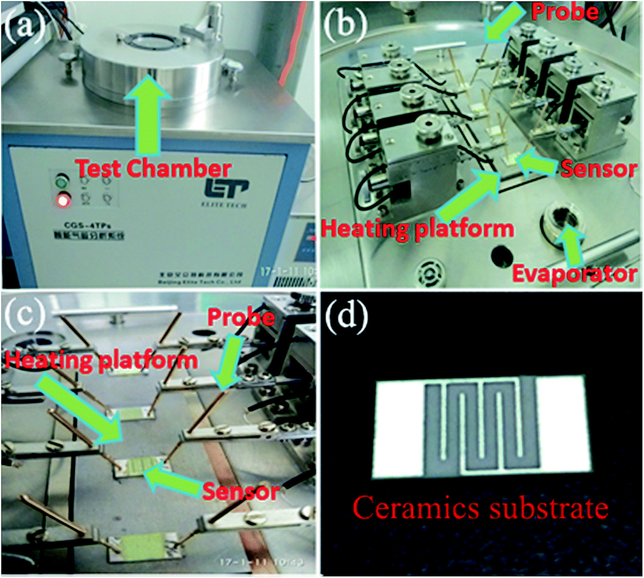 | ||
| Fig. 1 The CGS-4TP intelligent gas sensing analysis system: (a) test chamber; (b) test system in the chamber; (c) probe, sensor and heating plating platform; (d) ceramics substrate. | ||
3. Results and discussion
The phase composition and crystal structures of the synthesized pure WO3 nanofibers and NiO–WO3 heterojunction nanofibers were studied using XRD, as displayed in Fig. 2(a). A series of strong diffraction peaks are observed for all curves, which are agreed well with the crystalline monoclinic WO3 phase (JCPDS, no. 43-1035), indicating that all samples show a high degree of crystallinity after calcination. Not only in the pure WO3, but also in all the samples, there are no other crystal phases or impurities detected within XRD detection limit (5%). The absence of NiO signals in XRD for the NiO–WO3 nanofibers is probably attributed to the low concentration and high dispersion of NiO in WO3 body.44,45 Moreover, for all NiO–WO3 composite nanofibers, the diffraction peaks are broadened compared with those of the pure WO3, indicating the decreased crystallite sizes for composite nanofibers. The mean grain sizes of different products were calculated through Scherrer equation.46 As demonstrated in Fig. 2(b), the mean grain sizes of pure WO3, 1%, 3% and 5 mol% NiO–WO3 composite nanofibers are 13.4, 8.5, 8.0, and 10.0 nm, respectively. Obviously, the NiO–WO3 composite nanofibers have a smaller grain size compared with pure WO3. This should be ascribed to that NiO phase inhibits the grain growth of WO3 during the heat treatment process. This inhibition effect is expected to increase with increasing Ni content. Nonetheless, at high Ni content, the aggregation of NiO nanocrystallites is unavoidable, leading to the decline of the inhibition effect. Consequently, the 5 mol% NiO–WO3 nanofibers have larger grain size than that of 1% and 3% nanofibers. Smaller of the mean grain size, more oxygen species can be adsorbed on the surface of nanofibers.44,47 This will be further supported by the subsequent XPS results in Fig. 3, where the 3 mol% NiO–WO3 nanofibers have much higher oxygen species absorbing capacity, which may be benefit to the sensor performance.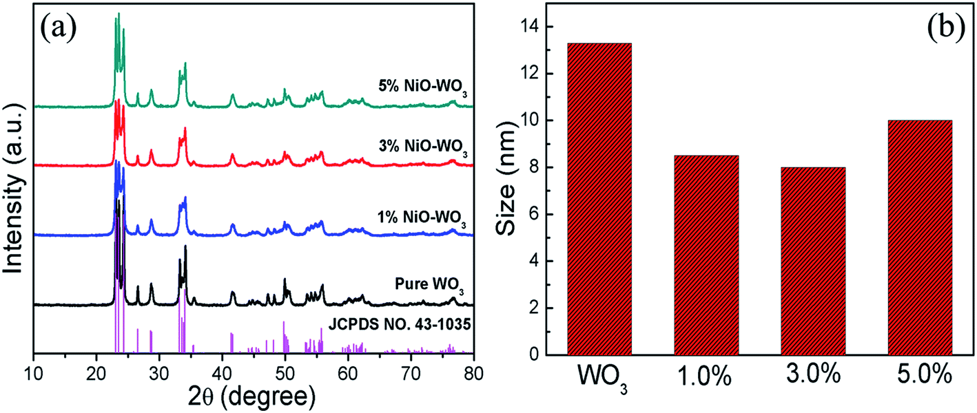 | ||
| Fig. 2 (a) XRD patterns of pure WO3 nanofibers and NiO–WO3 composite nanofibers and (b) the size distributions of different samples. | ||
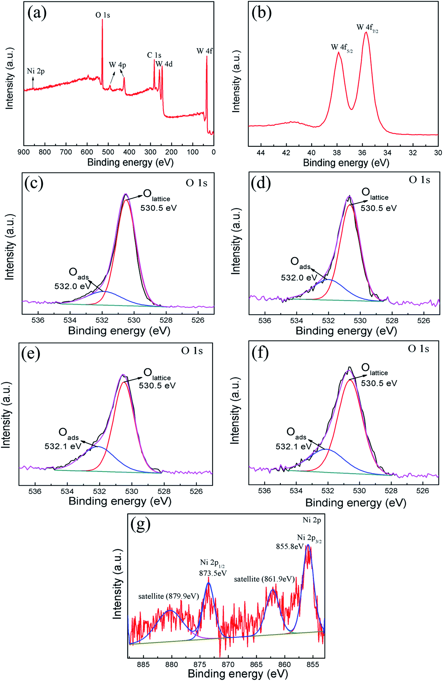 | ||
| Fig. 3 XPS analysis of pure WO3 and NiO–WO3 composite nanofibers: (a) survey spectrum and high resolution spectra for (b) W 4f region and (g) Ni 2p region of 3 mol% NiO–WO3 composite nanofibers; high resolution spectra for O 1s region of (c) pure WO3, (d) 1 mol%, (e) 3 mol% and (f) 5 mol% NiO–WO3 composite nanofibers. | ||
The XPS spectra were measured to further investigate the chemical states of W and Ni, and analyze the surface oxygen species of pure WO3 and NiO–WO3 heterojunction nanofibers. A wide survey scan clearly indicates that the main constituent elements are W, O, C and Ni in the 3 mol% NiO–WO3 heterojunction nanofibers [see Fig. 3(a)]. The peaks of W 4f spectrum at 37.8 eV and 35.6 eV correspond to W 4f5/2 and W 4f7/2, respectively [Fig. 3(b)], suggesting a normal state of W6+ in the heterojunction nanofibers.36,45 In addition, the O 1s peaks of pure and heterojunction nanofibers are asymmetric and can be deconvoluted into two main components located at 530.5 and 532.0/532.1 eV by fitting with the Gaussian function, as shown in Fig. 3(c)–(f). The intense peak with lower binding energy can be associated with the O 1s core level of the lattice oxygen (OLattice) in the metal oxides (WO3 or NiO). The peak with higher binding energy is proposed to be the chemically adsorbed oxygen (Oads) on the grain surfaces.48–50 Moreover, we can assess the oxygen species absorbing capacity according to the intensity of Oads component in the O 1s peak.51 The Oads component relative percentages of the pure WO3, 1 mol%, 3 mol%, and 5 mol% NiO–WO3 are 20.5%, 34.0%, 41.2% and 35.4%, respectively. Apparently, upon NiO introduction, the content of Oads component is markedly increased. In particular, 3 mol% NiO–WO3 heterojunction nanofibers have the highest content of Oads. As we all know, the gas sensing performance of nanomaterials is related to the capability of chemisorbed oxygen. Thus, such a high percentage of Oads content in the NiO–WO3 heterojunction nanofibers will undoubtedly benefit the enhancement of sensing performance. Fig. 3(g) shows the high resolution XPS spectrum of Ni 2p in the 3% NiO–WO3 nanofibers, where two groups of peaks located at 851–867 and 868–885 eV are revealed, corresponding to the characteristic peaks of Ni 2p3/2 and Ni 2p1/2, respectively.52 It is seen that the Ni 2p3/2 and Ni 2p1/2 main peaks are centered at 855.8 and 873.5 eV, respectively. Moreover, two extra Ni 2p3/2 and Ni 2p1/2 satellite peaks are also observed at 861.9 and 879.9 eV, respectively. The above results are consistent with the previous reports, further confirming the presence of NiO in the heterojunction nanofibers.53,54
The morphologies of synthesized products investigated by SEM are shown in Fig. 4(a)–(e). It can be observed that all products are composed of a large number of continuous 1D nanofibers. Compared with pure WO3 nanofibers [Fig. 4(a)], the NiO–WO3 composite nanofibers have smaller mean diameter, as can be seen from Fig. 4(b)–(d) for 1 mol%, 3 mol%, 5 mol% NiO–WO3 nanofibers, respectively. Moreover, one can see that the NiO–WO3 heterojunction nanofibers are obviously rougher compared with the pure WO3, which suggests that the NiO–WO3 heterojunction nanofibers are beneficial to the gas adsorption and diffusion. The SEM image of pure NiO are also described in Fig. 4(e), showing the fiber-like morphology. EDX spectroscopy [Fig. 4(f)] indicates that W, O, Ni, and Al elements are detected in the 3 mol% NiO–WO3 heterojunction nanofibers, where Al element in EDX spectrum is from Al substrate.
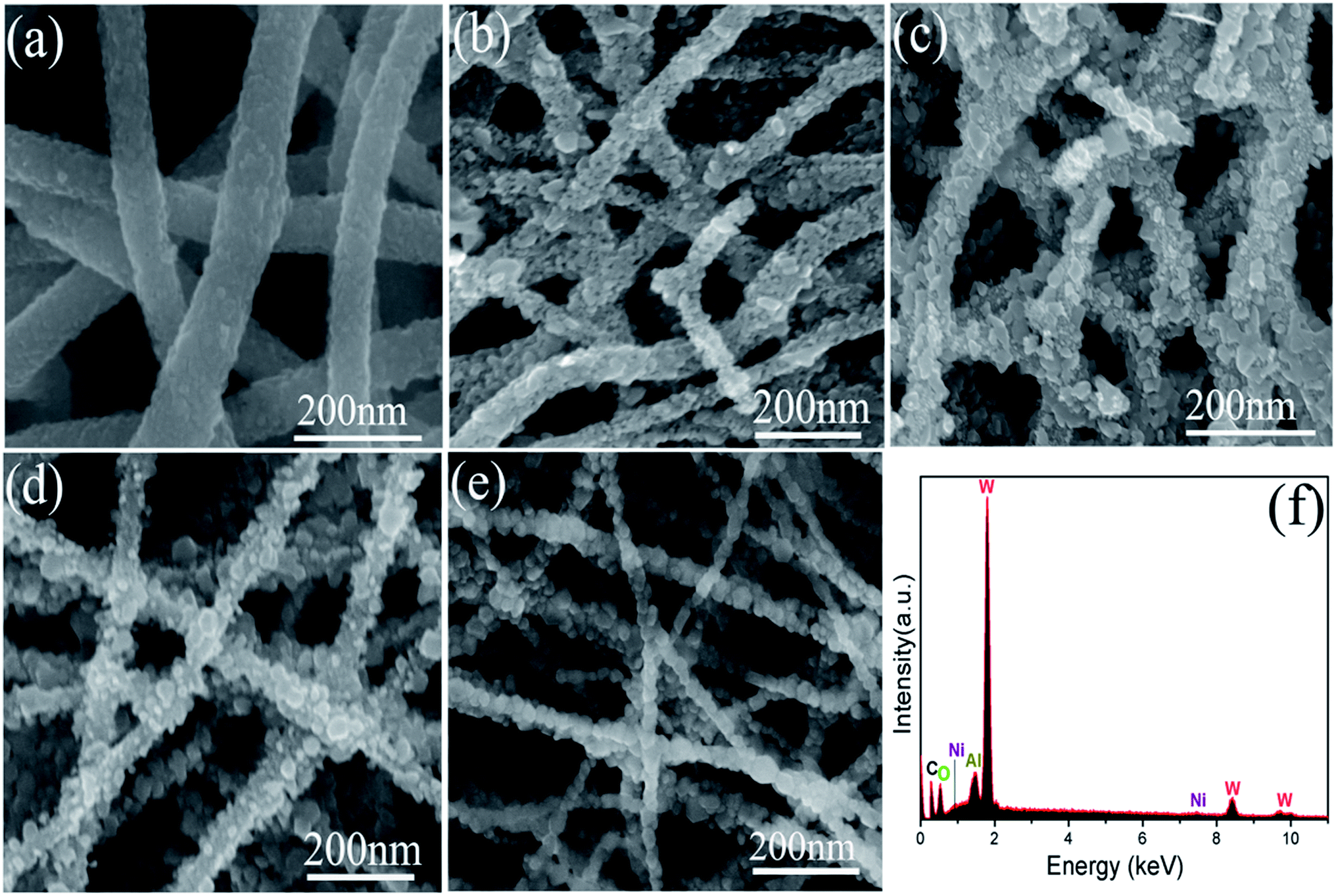 | ||
| Fig. 4 (a) SEM image of pure WO3; SEM images of the NiO–WO3 composite nanofibers with different Ni contents: (b) 1 mol%, (c) 3 mol%, (d) 5 mol%; (e) SEM image of pure NiO; (f) EDX spectrum of 3 mol% NiO–WO3 composite nanofibers. | ||
The 3 mol% heterojunction nanofibers are confirmed to have the smallest mean grain size and highest percentage of Oads content. Accordingly, an enhanced sensing performance of the 3 mol% heterojunction nanofibers may be expected. Therefore, TEM and high-resolution TEM (HRTEM) measurements were performed to further investigate the microstructure of the 3 mol% heterojunction nanofibers. Fig. 5(a) displays the TEM image of an individual NiO–WO3 nanofiber. The nanofiber is composed of many nanoparticles. Rough morphology and porous structure are also clearly revealed. HRTEM [Fig. 5(b)] observation reveals that the measured fringe spacing is about 0.24 nm, corresponding to the (111) plane of the cubic NiO. The fringe spacings of 0.36 nm and 0.38 nm, corresponding to the (200) and (222) crystal planes of monoclinic WO3, respectively, are also recognized.
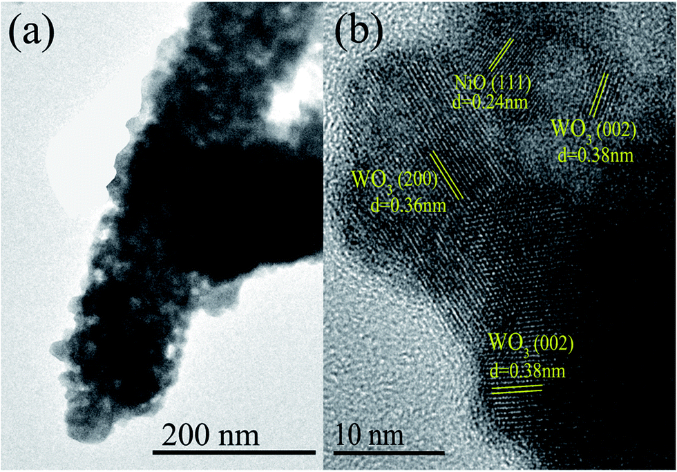 | ||
| Fig. 5 (a) TEM and (b) HRTEM image of a typical NiO–WO3 composite nanofiber with 3 mol% NiO. | ||
The surface areas and porous structures of the pure WO3 and 3 mol% NiO–WO3 heterojunction nanofibers were examined by the nitrogen adsorption–desorption measurements. As shown in Fig. 6(a), a clear hysteresis loop is observed, suggesting the existence of abundant mesoporous structures in the nanofibers. The BET surface areas of the pure WO3 and 3% NiO–WO3 nanofibers are calculated to be 11.40 and 19.49 m2 g−1, respectively. Fig. 6(b) shows the corresponding pore-size distribution curves of the two samples. The pure WO3 nanofibers have a pore-size distribution centered at 7.95 nm, while the 3 mol% NiO–WO3 nanofibers exhibit an increased pore-size distribution at 15.26 nm. These results together with the TEM analysis indicate that the 3 mol% NiO–WO3 heterojunction nanofibers possess higher specific surface area and more porous structure, which are beneficial to the efficient gas absorption and diffusion.
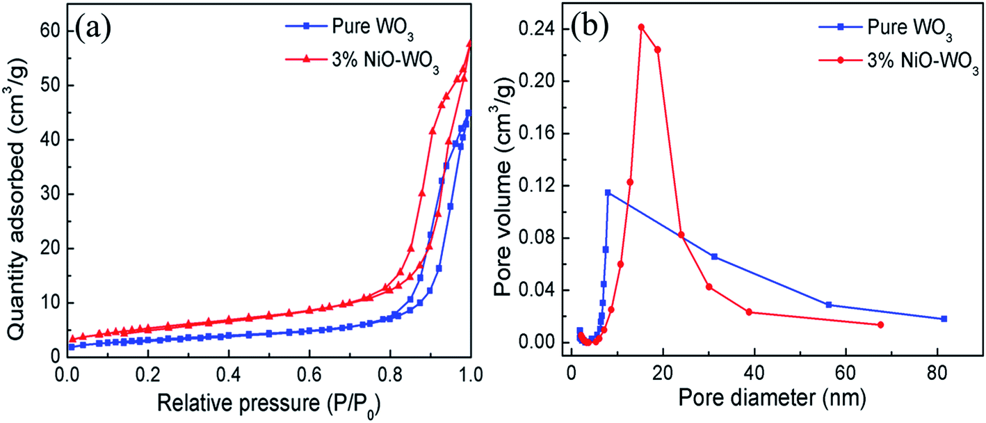 | ||
| Fig. 6 (a) Nitrogen absorption–desorption isotherms curves and (b) pore size distribution curves of pure WO3 and 3 mol% NiO–WO3 composite nanofibers. | ||
It is well accepted that the gas sensing properties of semiconductors are significantly affected by the working temperature, because the content of ionized oxygen species (O2−, O−, O2−) on the surfaces of semiconductors is greatly related to the temperature,55,56 accordingly resulting in the change of sensor resistance. Fig. 7 shows sensing response towards acetone as a function of working temperature for all sensors. One can see that NiO–WO3 heterojunction nanofibers exhibit higher response (Ra/Rg) than that of pristine WO3 and NiO nanofibers in all temperature range. Particularly, the largest sensitivity to acetone is demonstrated for the sensor based on the 3 mol% NiO–WO3 nanofibers at almost all measured temperatures. In addition, the temperature dependent response characteristic for all sensors exhibits a typical mountain-shaped curve.57 The responses of all sensors increase to maximum values at 375 °C, and then decrease as the operating temperature increases further. Accordingly, the optimum operating temperature is determined to be 375 °C for all sensors in the following sensing tests.
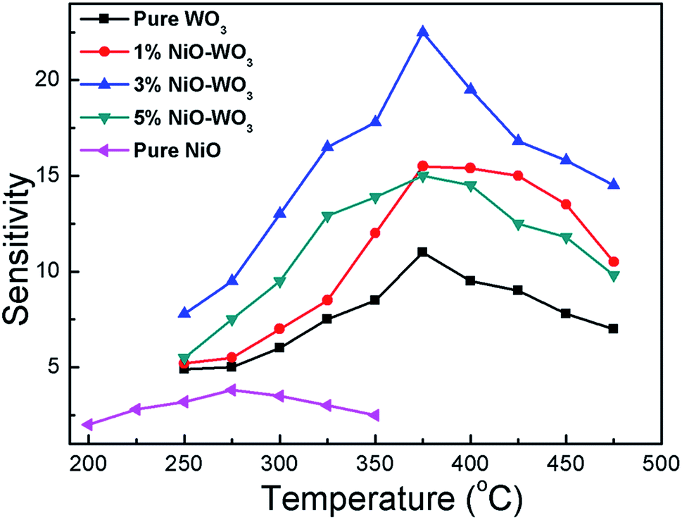 | ||
| Fig. 7 Responses of sensors based on the pure WO3, NiO–WO3 composite nanofibers, and pure NiO nanofibers to 100 ppm acetone as a function of the operating temperature. | ||
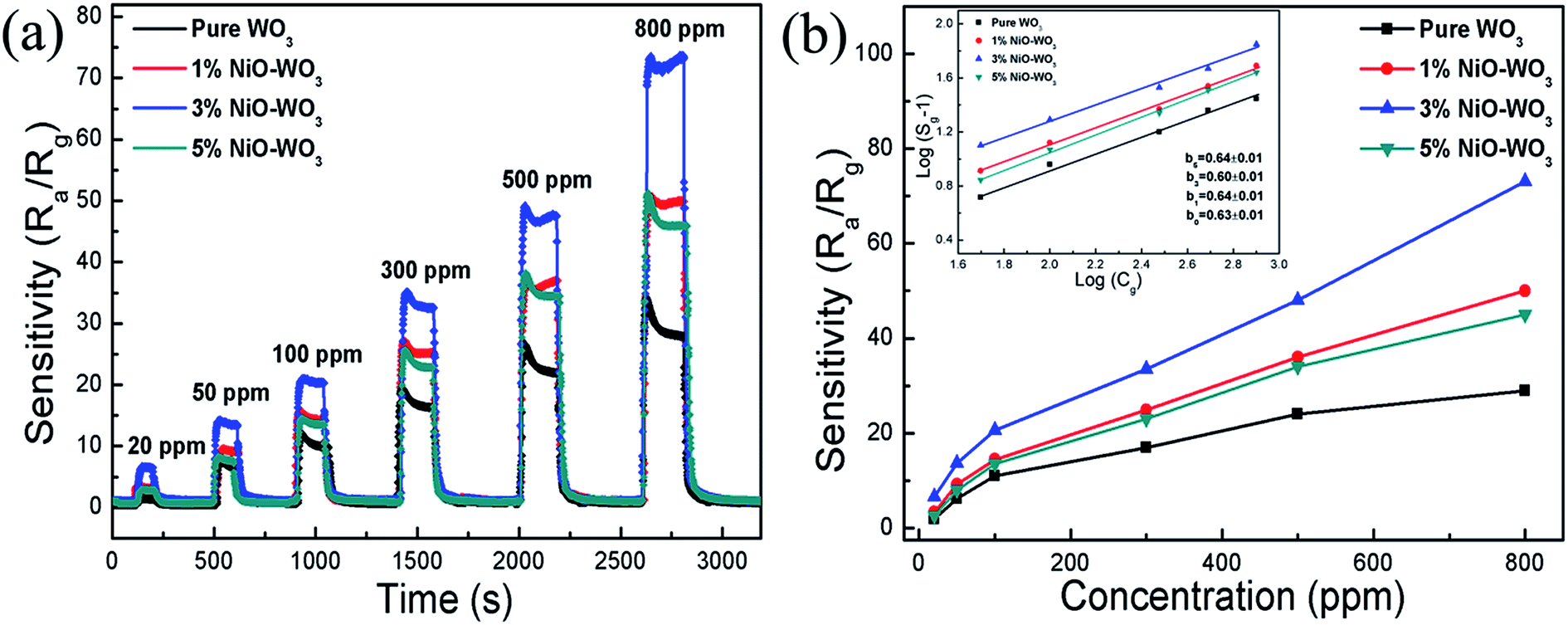
Fig. 8(a) illustrates the dynamic gas-sensing characteristics for all sensors upon exposure to different acetone concentrations (20–800 ppm) at 375 °C. Fig. 8(b) shows the corresponding response value as a function of acetone concentration for all sensors. We can see clearly that the response of all sensors is increased distinctly as the acetone concentration increases. For example, when the acetone concentrations are 20, 50, 100, 300, 500, and 800 ppm, the response values of the sensors constructed by the 3 mol% NiO–WO3 heterojunction nanofibers are 6.6, 13.7, 22.5, 33.5, 48, and 73, respectively. Generally, the sensor response (Sg) and the target gas concentration (Cg) have the following relationship:
| Sg = 1 + a[Cg]b | (1) |
|
log(Sg − 1) = blog(Cg) + log(a)
| (2) |
 | ||
| Fig. 8 (a) Dynamic gas-sensing characteristics of the sensors based on different samples under various gas concentrations and (b) the corresponding response value on acetone gas concentration at 375 °C. | ||
It can be seen that b can be easily calculated from the slope of the corresponding log(Sg − 1) ∼ log(Cg) curve. The inset in Fig. 8(b) shows the good linear relation between the log(Sg − 1) and log(Cg) for all sensors. The values of the slope b are determined to be about 0.63, 0.64, 0.60, and 0.64 for the pure WO3, 1 mol%, 3 mol%, and 5 mol% NiO–WO3 nanofibers, respectively. All the b values are relatively close to 0.5, indicating that O2− is the dominating oxygen species absorbed on the pristine WO3 and NiO–WO3 heterojunction nanofibers.
The response–recovery curves of the four kinds of sensors towards 100 ppm acetone at 375 °C are further described in Fig. 9(a). The response times are calculated to be 10, 7, 6, and 6 s, while the recovery times are evaluated to be 15, 12, 11, and 11 s, for the pure WO3, 1 mol%, 3 mol%, and 5 mol% NiO–WO3 sensors, respectively, as displayed in Fig. 9(b). This demonstrates that compared with the pure WO3, the NiO–WO3 heterojunction nanofibers have shorter response and recovery times. These improved response and recovery times may be ascribed to the special porous structure of the NiO–WO3 nanofibers, which is beneficial to a fast absorption and desorption of gas molecules.
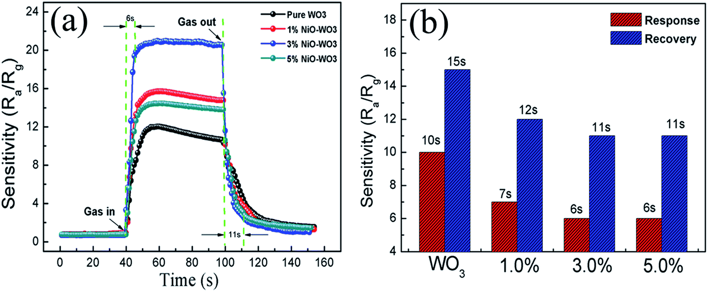 | ||
| Fig. 9 (a) Response–recovery curves of the pure WO3 and NiO–WO3 gas sensors to 100 ppm acetone at 375 °C and (b) the response and recovery times of all sensors to acetone. | ||
Fig. 10 exhibits the selectivity of the pristine WO3 and NiO–WO3 sensors to other interfering gases, such as ethanol (C2H5OH), methylbenzene (C7H8), acetic acid (CH3COOH), iso-propyl alcohol (C3H8O), ammonia (NH3), and methyl alcohol (CH3OH) at 100 ppm concentration. Obviously, the sensor based on 3 mol% NiO–WO3 heterojunction nanofibers exhibits the highest response value of 22.5 to 100 ppm acetone, whereas the responses to other gases are less than 9. In addition, the relative increase of response value to acetone upon the introduction of NiO is 93.04%, which is also the highest. These results demonstrate the prominent selectivity to acetone of the 3 mol% NiO–WO3 sensor. It is noted that the relative increase to NH3 is up to 81.82%, indicating that the adding of NiO also improves the selectivity of NH3. The excellent selectivity may be due to the different gas reaction processes and different energies needed to react with the adsorbed active oxygen species (O2−) on the surface of NiO–WO3 nanofibers. At the optimum operating temperature of 375 °C, some gases may escape from the surface of NiO–WO3 nanofibers and other gases may not react fully with adsorbed O2− species because of insufficient energy.60
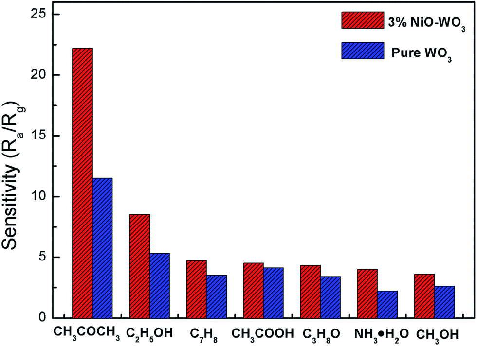 | ||
| Fig. 10 Selectivity of pure WO3 and 3 mol% NiO–WO3 gas sensors to different gases under a concentration of 100 ppm at 375 °C. | ||
The long-term stabilities of the sensors constructed by the pure WO3 and 3 mol% NiO–WO3 nanofibers were also investigated, as displayed in Fig. 11. The tests were performed at 375 °C to 100 ppm acetone over 20 days. The results indicate that the response values based on pure WO3 and NiO–WO3 sensors are fluctuated lightly around 22.5 and 11, respectively, confirming the good stabilities of both the pure and heterojunction nanofiber based sensors.
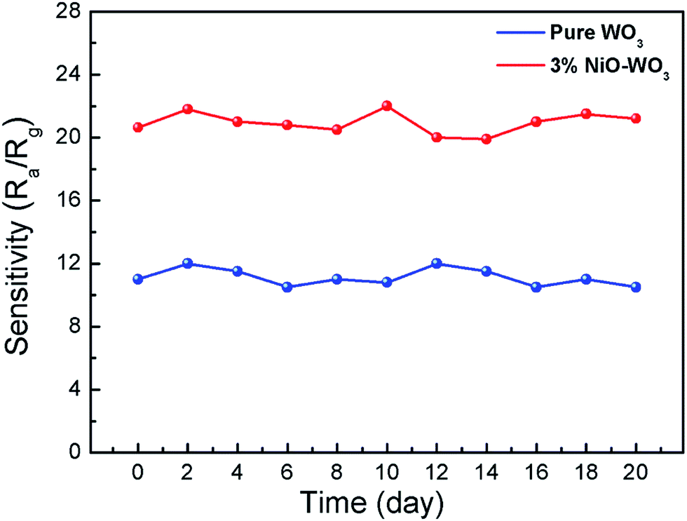 | ||
| Fig. 11 Long-term stabilities of gas sensors based on the pure WO3 and 3 mol% NiO–WO3 composite nanofibers at 375 °C. | ||
4. Proposed sensing mechanism
It is well known that the sensing mechanism of the metal oxides is in close relation to the resistance change caused by the adsorption of oxygen species and reaction with test gas molecules on the surface.61 As illustrated in Fig. 12(a), when the sensor is exposed to air, ionized oxygen species (O2−) is formed on the surface of the WO3 nanofibers at high temperature (375 °C) by transferring the electrons from the conduction band of WO3 to chemisorbed oxygen. This leads to the generation of an electron depletion layer near the surface of WO3. When acetone is introduced, the surface reaction occurs between CH3COCH3 and active O2− species on the surface of WO3 nanofibers, according to the following equation:58| CH3COCH3 (gas) + 8O2− → 3CO2 + 3H2O + 16e− | (3) |
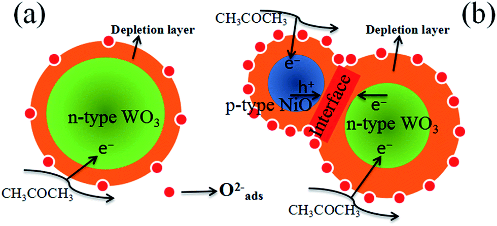 | ||
| Fig. 12 Schematic model of (a) pure WO3 and (b) p-type NiO/n-type WO3 heterojunction based sensor when exposed to acetone vapor. | ||
This process results in a decrease of the sensor resistance because a large quantity of trapped electrons are released back to the conductance band of WO3. This low resistance state goes back to the original high resistance state when the sensor is exposed to air again.
By comparison, our experimental results illustrate that compared with the pure WO3, the NiO–WO3 composite nanofibers possess obviously enhanced sensing performances towards acetone. The sensing enhancement mechanism here can be attributed to the several following reasons. The first one is the generation of p–n junctions at the interfaces between p-type NiO and n-type WO3. This enhancement mechanism was also responsible for the improved gas response for NiO–SnO2,8 CuO–SnO2,62 CuO–SnO2,63 and Co-doped SnO2,64 composites in previous reports. In our case, NiO is a p-type semiconductor and WO3 is a n-type semiconductor.65,66 When p-type NiO nanocrystals are introduced into n-type WO3, many p–n junctions should be formed at the interfaces between the NiO and WO3. The transferring of electrons from WO3 to NiO occurs due to that the Fermi level of p-type NiO is much higher than that of n-type WO3. Simultaneously, the migration of holes also happens from NiO to WO3, and an equalization of these two Fermi levels is finally obtained.67 As a result, a new wider electron depletion layer is created at the surface/interface of NiO/WO3 p–n junctions [Fig. 12(b)], which leads to further increase in sensor resistance. According to our test results, the resistance in air of the pure WO3 sensor and 3 mol% NiO–WO3 sensor are 0.26 MΩ and 58.00 MΩ at 375 °C, respectively. This remarkable increase of resistance illustrates the successful generation of p–n junctions in the NiO–WO3 composites. The formation of p–n junctions with thick electron depletion layer contributes largely to the improved sensing performances of NiO–WO3 sensor.
The second aspect should be originated from the high oxygen species absorbing capacity of the 3 mol% NiO–WO3 nanofibers. Previous report has shown that a full monolayer of oxygen species can be effectively absorbed on the surface of p-type NiO,68 demonstrating the particularly high oxygen species absorbing capacity of NiO nanoparticles. Therefore, the adding of p-type NiO nanoparticles into the WO3 matrix contributes greatly to the improved oxygen absorbing capacity of the NiO–WO3 composites. The increased oxygen absorption species can lead to the further widening of the electron depletion layer, as can be seen in the schematic diagram [Fig. 12(b)]. The increased content of active O2− species is responsible for the further improvement of the sensing performances of the NiO–WO3 composites.
Last but not least, the special pores and rough surface structural features are also accountable for the sensing improvement of the 3 mol% NiO–WO3 heterojunction nanofibers. On the one hand, due to the large pores, the oxygen and acetone molecules can be diffused rapidly in the sensing layer,69 leading to a fast response and recovery times of the NiO–WO3 sensor. On the other hand, more oxygen molecules can be absorbed and ionized due to the high surface area and small particle size of NiO–WO3 heterojunction nanofibers. Therefore, the modulation of electron depletion layer can be further enhanced,70,71 leading to the high response of the 3 mol% NiO–WO3 sensor.
Our results show that the nanofibers possess the smallest mean grain size and highest percentage of Oads content at a Ni content of 3 mol%, which is responsible for the best gas sensing performances of the 3 mol% for NiO–WO3 heterojunction nanofibers.
5. Conclusions
In summary, pure WO3 and NiO–WO3 composite nanofibers with different molar ratios (Ni/W = 0%, 1%, 3% and 5%) were successfully produced by an electrospinning and calcination technique. The gas sensing results indicated that porous NiO–WO3 heterojunction nanofibers displayed larger sensitivity, faster response, and shorter recovery time towards acetone compared with the pure WO3 nanofibers. Particularly, the 3 mol% NiO–WO3 heterojunction nanofibers exhibited the largest response to 100 ppm acetone, showing an excellent response value of 22.5 at the operating temperature of 375 °C, which is almost 2.1 times larger than that of the pure WO3 nanofibers. In addition, excellent selectivity and long-term stability to acetone were also demonstrated for the 3 mol% NiO–WO3 sensor. The combined effects including the generation of p–n junctions between NiO and WO3, high oxygen species absorbing capacity, and special porous structural features with high surface area and small grain size, were accountable for the enhanced sensing properties of the 3 mol% NiO–WO3 heterojunction nanofibers.Conflicts of interest
There are no conflicts to declare.Acknowledgements
This work was supported by the Science and Technology Program of Shaanxi Province (No. 2016KJXX-15) and the Fundamental Research Funds for the Central Universities (No. GK201602006).References
- K. Wetchakun, T. Samerjai, N. Tamaekong, C. Liewhiran, C. Siriwong, V. Kruefu, A. Wisitsoraat, A. Tuantranont and S. Phanichphant, Sens. Actuators, B, 2011, 160, 580–591 CrossRef CAS.
- M. Utriainen, E. Kärpänoja and H. Paakkanen, Sens. Actuators, B, 2003, 93, 17–24 CrossRef CAS.
- E. Schaller, J. O. Bosset and F. Escher, LWT--Food Sci. Technol., 1998, 31, 305–316 CrossRef CAS.
- A. P. Turner and N. Magan, Nat. Rev. Microbiol., 2004, 2, 161–166 CrossRef CAS PubMed.
- R. J. Lü, W. Zhou, K. Y. Shi, Y. Yang, L. Wang, K. Pan, C. G. Tian, Z. Y. Ren and H. G. Fu, Nanoscale, 2013, 5, 8569–8576 RSC.
- E. Tolmachoff, S. Memarzadeh and H. Wang, J. Phys. Chem. C, 2011, 115, 21620–21628 CAS.
- S. Singkammo, S. Wisitsoraat, C. Sriprachuabwong, A. Tuantranont, S. Phanichphant and C. Liewhiran, ACS Appl. Mater. Interfaces, 2015, 7, 3077–3092 CAS.
- Y. Chen, L. Yu, D. Feng, M. Zhuo, M. Zhang, E. Zhang, Z. Xu, Q. Li and T. Wang, Sens. Actuators, B, 2012, 166–167, 61–67 CrossRef CAS.
- X. Liu, J. Zhang, X. Guo, S. Wu and S. Wang, Sens. Actuators, B, 2011, 152, 162–167 CrossRef CAS.
- A. Chowdhuri, V. Gupta, K. Sreenivas, R. Kumar, S. Mozumdar and P. K. Patanjali, Appl. Phys. Lett., 2004, 84, 1180–1182 CrossRef CAS.
- Y. Zhang, J. Q. Xu, Q. Xiang, H. Li, Q. Y. Pan and P. C. Xu, J. Phys. Chem. C, 2009, 113, 3430–3435 CAS.
- Y. H. Xiao, L. Z. Lu, A. Q. Zhang, Y. H. Zhang, L. Sun, L. Huo and F. Li, ACS Appl. Mater. Interfaces, 2012, 4, 3797–3804 CAS.
- J. Guo, J. Zhang, M. Zhu, D. Ju, H. Xu and B. Cao, Sens. Actuators, B, 2014, 199, 339–345 CrossRef CAS.
- S. J. Kim, S. J. Choi, J. S. Jang, N. H. Kim, M. Hakim, H. L. Tuller and I. D. Kim, ACS Nano, 2016, 6, 5891–5899 CrossRef PubMed.
- N. H. Kim, S. J. Choi, D. J. Yang, J. Bae, J. Park and I. D. Kim, Sens. Actuators, B, 2014, 193, 574–581 CrossRef CAS.
- J. Kim, M. Kim, M. S. Lee, K. Kim, S. Ji, Y. T. Kim, J. Park, K. Na, K. H. Bae, H. K. Kim, F. Bien, C. Y. Lee and J. U. Park, Nat. Commun., 2017, 8, 14997 CrossRef PubMed.
- J. Park, J. Kim, K. Kim, S. Y. Kim, W. H. Cheong, K. Park, J. H. Song, G. H. Namgoong, J. J. Kim, J. Heo, F. Bien and J. U. Park, Nanoscale, 2016, 8, 10591–10597 RSC.
- K. Lee, J. Park, M. S. Lee, J. Kim, B. G. Hyun, D. J. Kang, K. Na, C. Y. Lee, F. Bien and J. U. Park, Nano Lett., 2014, 14, 2647–2654 CrossRef CAS PubMed.
- L. Saadi, C. L. Mauriat, V. Oison, H. Ouali and R. Hayn, Appl. Surf. Sci., 2014, 293, 76–79 CrossRef CAS.
- Y. Li, W. Luo, N. Qin, J. Dong, J. Wei and W. Li, Angew. Chem., Int. Ed., 2014, 53, 9035–9040 CrossRef CAS PubMed.
- T. A. Ho, T. S. Jun and Y. S. Kim, Sens. Actuators, B, 2013, 185, 523–529 CrossRef CAS.
- C. Feng, C. Wang, P. Cheng, X. Li, B. Wang, Y. Guan, J. Ma, H. Zhang, Y. Sun, P. Sun, J. Zheng and G. Lu, Sens. Actuators, B, 2015, 221, 434–442 CrossRef CAS.
- N. H. Kim, S. J. Choi, S. J. Kim, H. J. Cho, J. S. Jang, W. T. Koo, M. Kim and I. D. Kim, Sens. Actuators, B, 2016, 224, 185–192 CrossRef CAS.
- C. H. Feng, X. Li, J. Ma, Y. F. Sun, C. W. P. Sun, J. Zheng and G. Y. Lu, Sens. Actuators, B, 2015, 209, 622–629 CrossRef CAS.
- W. Cao and Y. Duan, Clin. Chem., 2006, 52, 800–811 CAS.
- C. Dong, X. Liu, H. Guan, G. Chen, X. Xiao, I. Djerdj and Y. Wang, Mater. Chem. Phys., 2016, 184, 155–161 CrossRef CAS.
- J. Shi, G. Hu, Y. Sun, M. Geng, J. Wu, Y. Liu, M. Ge, J. Tao, M. Cao and N. Dai, Sens. Actuators, B, 2011, 156, 820–824 CrossRef CAS.
- X. Chi, C. Liu, L. Liu, Y. Li, Z. Wang, X. Bo, L. Liu and C. Su, Sens. Actuators, B, 2014, 194, 33–37 CrossRef CAS.
- S. Wei, G. Zhao, W. Du and Q. Tian, Vacuum, 2016, 124, 32–39 CrossRef CAS.
- R. Xing, Y. Du, X. Zhao and X. Zhang, Sensors, 2017, 17, 710 CrossRef PubMed.
- F. Yang and Z. Guo, Mater. Lett., 2017, 203, 93–96 CrossRef CAS.
- M. Yin, L. Yu and S. Liu, J. Alloys Compd., 2017, 696, 490–497 CrossRef CAS.
- G. Xie, J. Yu, X. Chen and Y. Jiang, Sens. Actuators, B, 2007, 123, 909–914 CrossRef CAS.
- T. Samerjai, N. Tamaekong, C. Liewhiran, A. Wisitsoraat, A. Tuantranont and S. Phanichphant, Sens. Actuators, B, 2011, 157, 90–297 CrossRef.
- M. U. Qadri, A. F. Diaz, M. Cittadini, A. Martucci, M. C. Pujol and J. F. Borrull, Sensors, 2014, 14, 11427–11443 CrossRef CAS PubMed.
- J. X. Zhao, Y. L. Cheng, X. Yan, D. F. Sun, F. L. Zhu and Q. J. Xue, CrystEngComm, 2012, 14, 5879–5885 RSC.
- H. Steinebach, S. Kannan, L. Rieth and F. Solzbacher, Sens. Actuators, B, 2010, 151, 162–168 CrossRef CAS.
- P. Rai, J. Yoon, H. Jeong, S. Hwang, C. Kwak and J. Lee, Nanoscale, 2014, 6, 8292–8299 RSC.
- Y. Zhang, L. Z. Xie, C. X. Yuan, C. L. Zhang, S. Liu, Y. Q. Peng, H. R. Li and M. Zhang, J. Mater. Sci.: Mater. Electron., 2016, 27, 1817–1827 CrossRef CAS.
- M. Tonezzer, D. T. T. Le, T. Q. Huy and S. Iannotta, Sens. Actuators, B, 2016, 236, 1011–1019 CrossRef CAS.
- C. Yuan, H. Li, L. Xie, F. Wang, H. Deng, F. Chang and Y. Sun, RSC Adv., 2015, 5, 92128–92133 RSC.
- M. Bao, Y. Chen, F. Li, J. Ma, T. Lv, Y. Tang, L. Chen, Z. Xu and T. Wang, Nanoscale, 2014, 6, 4063–4066 RSC.
- W. Noh, Y. Shin, J. Kim, W. Lee, K. Hong, S. A. Akbar and J. Park, Solid State Ionics, 2002, 152, 827–832 CrossRef.
- Z. Lin, N. Li, Z. Chen and P. Fu, Sens. Actuators, B, 2017, 239, 501–510 CrossRef CAS.
- Y. Sun, L. Chen, Y. Wang, Z. Zhao, P. Li, W. Zhang, Y. L. Wang and J. Hu, J. Mater. Sci., 2017, 52, 1561–1572 CrossRef CAS.
- W. X. Jin, S. Y. Ma, Z. Z. Tie, J. J. Wei, J. Luo and X. H. Jiang, Sens. Actuators, B, 2015, 213, 171–180 CrossRef CAS.
- L. Liu, S. C. Li, L. Y. Wang, C. C. Guo, Q. G. Dong and W. Li, J. Am. Ceram. Soc., 2011, 94, 771–775 CrossRef CAS.
- C. J. Dong, X. Liu, H. T. Guan, G. Chen, X. C. Xiao, I. Djerdj and Y. D. Wang, Mater. Chem. Phys., 2016, 184, 155–161 CrossRef CAS.
- W. Y. Jung and S. S. Hong, J. Ind. Eng. Chem., 2013, 19, 157–160 CrossRef CAS.
- C. P. Gu, Y. W. Cui, L. Y. Wang, E. Sheng, J. J. Shim and J. R. Huang, Sens. Actuators, B, 2017, 241, 298–307 CrossRef CAS.
- X. Wang, P. R. Ren, H. L. Tian, H. Q. Fan, C. L. Cai and W. G. Liu, J. Alloys Compd., 2016, 669, 29–37 CrossRef CAS.
- Z. L. Gu, D. Bin, Y. Feng, K. Zhang, J. Wang, B. Yan, S. M. Li, Z. P. Xiong, C. Q. Wang, Y. Shiraishi and Y. K. Du, Appl. Surf. Sci., 2017, 411, 379–385 CrossRef CAS.
- H. C. Liu, Q. Zhou, Q. Y. Zhang, C. X. Hong, L. Xu, L. F. Jin and W. G. Chen, Sensors, 2017, 17, 913 CrossRef PubMed.
- W. X. Guo, W. W. Sun and Y. Wang, ACS Nano, 2015, 9, 11462–11471 CrossRef CAS PubMed.
- C. Wang, L. Yin, L. Zhang, D. Xiang and R. Gao, Sensors, 2010, 10, 2088–2106 CrossRef CAS PubMed.
- Y. V. Kaneti, Z. Zhang, J. Yue, Q. M. D. Zakaria, C. Chen, X. Jiang and A. Yu, Phys. Chem. Chem. Phys., 2014, 16, 11471–11480 RSC.
- N. Yamazoe, G. Sakai and K. Shimanoe, Catal. Surv. Asia, 2003, 7, 63–73 CrossRef CAS.
- M. Yin and S. Liu, Sens. Actuators, B, 2015, 209, 343–351 CrossRef CAS.
- Z. Wang, J. Xue, D. Han and F. Gu, ACS Appl. Mater. Interfaces, 2015, 7, 308–317 CAS.
- Z. W. Liu, B. Liu, W. Y. Xie, H. Li, R. Zhou, Q. H. Li and T. H. Wang, Sens. Actuators, B, 2016, 235, 614–621 CrossRef CAS.
- P. Sun, Y. Cai, S. Du, X. Xu, L. You, J. Ma, F. Liu, X. Liang, Y. Sun and G. Lu, Sens. Actuators, B, 2013, 182, 336–343 CrossRef CAS.
- X. Y. Xue, L. L. Xing, Y. J. Chen, S. L. Shi, Y. G. Wang and T. H. Wang, J. Phys. Chem. C, 2008, 112, 12157–12160 CAS.
- J. D. Choi and G. M. Choi, Sens. Actuators, B, 2000, 69, 120–126 CrossRef CAS.
- L. Liu, C. C. Guo, S. C. Li, L. Y. Wang, Q. G. Dong and W. Li, Sens. Actuators, B, 2010, 150, 806–810 CrossRef CAS.
- Y. Li, Z. Tang, J. Zhang and Z. Zhang, Appl. Catal., B, 2017, 207, 207–217 CrossRef CAS.
- H. Ohta, M. Hirano, K. Nakahara, H. Maruta, T. Tanabe, M. Kamiya, T. Kamiya and H. Hosono, Appl. Phys. Lett., 2003, 83, 1029–1031 CrossRef CAS.
- D. R. Miller, S. A. Akbar and P. A. Morris, Sens. Actuators, B, 2014, 204, 250–272 CrossRef CAS.
- K. Jain, R. P. Pant and S. T. Lakshmikumar, Sens. Actuators, B, 2006, 113, 823–829 CrossRef CAS.
- P. Sun, Z. Zhu, P. Zhao, X. Liang, Y. Sun, F. Liu and G. Lu, CrystEngComm, 2012, 14, 8335–8337 RSC.
- C. Xu, J. Tamaki, N. Miura and N. Yamazoe, Sens. Actuators, B, 1991, 3, 147–155 CrossRef CAS.
- M. Tiemann, Chem.– Eur. J., 2007, 13, 8376–8388 CrossRef CAS PubMed.
| This journal is © The Royal Society of Chemistry 2017 |