
 Open Access Article
 This Open Access Article is licensed under a Creative Commons Attribution-Non Commercial 3.0 Unported Licence
Half-metals and half-semiconductors in a transition metal doped SnSe2 monolayer: a first-principles study
Xuming Wua,
Jiangchao Hana,
Yulin Fenga,
Guanpeng Lia,
Cong Wanga,
Guangqian Dingb and
Guoying Gao *a
*a
aSchool of Physics and Wuhan National High Magnetic Field Center, Huazhong University of Science and Technology, Wuhan 430074, China. E-mail: guoying_gao@mail.hust.edu.cn
bSchool of Science, Chongqing University of Posts and Telecommunications, Chongqing, 400065, China
First published on 15th September 2017
Abstract
Recently, a new two-dimensional (2D) semiconductor SnSe2 monolayer has been grown by molecular beam epitaxy, and weak ferromagnetic behavior above room temperature in Mn-doped SnSe2 thin films was also observed experimentally. Here, using first-principles calculations, we investigate the structural, electronic, and magnetic properties of an SnSe2 monolayer doped with transition metals V, Cr, Mn, Fe, Co, Ni and Cu. The calculated formation energies indicate that it is energetically favorable and relatively easy to incorporate these transition metals except for Cu into the SnSe2 monolayer under Se-rich conditions. Doping induces considerable magnetic moments except for the Ni-doped system. Long-range ferromagnetic order is observed for V, Cr and Fe doping, and Mn doping has a short-range ferromagnetic order. Cu doping has an antiferromagnetic ground state. Within generalized gradient approximation, interestingly, both ferromagnetic V doping and metastable ferromagnetic Cu doping exhibit half-metallicity. Both Mn- and Fe-doped SnSe2 monolayers are half-semiconductors. These properties are governed by the transition metal 3d orbital splitting under the crystal field and p–d hybridization. Within hybrid functional or spin–orbit coupling, the V-doped SnSe2 monolayer becomes a half-semiconductor, and the Cu-doped SnSe2 monolayer is still a half-metal. These studies indicate the promising spintronic applications for 2D semiconductor SnSe2 doped by transition metals.
1. Introduction
In recent years, half-metallic magnets (HMMs)1 have attracted considerable research interest in spintronic applications, because their band structure is metallic in only one of the two spin channels (Fig. 1(a)), leading to 100% spin polarization of electrons around the Fermi level. So, HMMs have been seen as the most promising candidates for spin-injector materials, and they are the key materials used to fabricate spintronic devices such as spin valves, spin field effect transistors, and spin filters.2 Several classes of HMMs have been fabricated experimentally or predicted theoretically, e.g., Heusler alloys, metallic oxides, transition-metal pnictides and chalcogenides, etc.3–5 In addition to HMMs, half-semiconductors (HSCs)6 are also a class of spintronic materials with 100% spin polarization, because their conduction band and valence band are spin split with the conduction band minimum and valence band maximum possessing the same spin channel (Fig. 1(b)).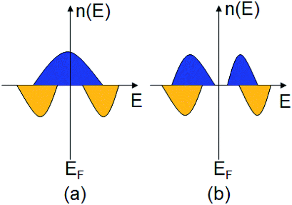 | ||
| Fig. 1 The schemes of density of states n(E) as a function of energy E for (a) a half-metal and (b) a half-semiconductor. Blue and yellow present the spin-up and spin-down states, respectively. | ||
Previous studies on HMMs and HSCs mainly focused on the bulk systems. Searching for HMMs and HSCs in graphene-like two-dimensional (2D) materials is interesting due to the advantages of ultrathin thickness (monolayer or few atomic layers), extraordinary electronic properties and facile synthesis. However, most of pristine graphene-like 2D materials have been found to be nonmagnetic, and several ones were predicted to be HMMs and HSCs.7–10 The emergence of magnetism in 2D materials usually needs external electric field, edge-functionalizing, vacancy, defect, strain and doping.8,11,12 Experimentally, substitutional doping has been proved to be a powerful route to induce ferromagnetism in some 2D materials such as Co and Cu-doped MoS2.13,14 Few HMMs and HSCs have been predicted in some MoS2-like 2D materials doped by transition metal (TM) atoms.15–17
Very recently, a new 2D semiconductor of SnSe2 monolayer has been grown by molecular beam epitaxy,18 and few-layer SnSe2 field effect transistor with a high current on/off ratio of 104 was also fabricated successfully.19 The studies on 2D SnSe2 mainly focused on the electronic and optoelectronic properties. Interestingly, a recent experiment revealed weak ferromagnetic behavior above room temperature in Mn-doped SnSe2 thin films, and importantly, even rather large concentrations of Mn (up to 0.6) do not destroy the 2D crystal structure of the parent SnSe2,20 which motivates us to search for HMMs and HSCs in 2D SnSe2 doped by Mn and other TM atoms. In this paper, we use the first-principles calculations to systemically investigate the electronic and magnetic properties of TM-doped SnSe2 monolayer (TM = V, Cr, Mn, Fe, Co, Ni, Cu). It is found that the structures of the doped systems except for Cu doping are energetically stable. Within generalized gradient approximation, both V- and Cu-doped SnSe2 monolayers exhibit half-metallicity, and both Mn- and Fe-doped SnSe2 monolayers are HSCs. Within hybrid functional or spin–orbit coupling, V-doped SnSe2 monolayer becomes a half-semiconductor, and Cu-doped SnSe2 monolayer is still a half-metal. These results indicate that TM-doped SnSe2 monolayers are promising candidates for 2D spintronic applications.
2. Computational details
The present work is performed by using the first-principles full-potential linearized augmented plane-wave method (Wien2k package)21 within the generalized gradient approximation (GGA) with the Perdew–Burke–Ernzerhof (PBE) scheme22 for the electronic exchange–correlation functional. We also consider the effects of hybrid functional and spin–orbit coupling on the electronic structures. The relativistic effect in the scalar approximation is considered. The radii Rmt of the muffin tins are chosen to be approximately proportional to the corresponding ionic radii and as large as possible under the condition that the spheres do not overlap. The RmtKmax relating to the energy cutoff is taken as 8.5. We adopt the 12 × 12 × 1 k meshes in the Brillouin zone integration. The self-consistency calculations are considered to be achieved when the total energy difference between succeeding iterations is less than 10−5 Ry per formula unit.SnSe2 bulk has the layered CdI2-type (T-type) structure with the space group of P![[3 with combining macron]](https://www.rsc.org/images/entities/char_0033_0304.gif) m1 and the in-plane lattice constant of 3.81 Å.23 For the structural model of TM-doped SnSe2 monolayer, we adopt the 4 × 4 × 1 supercell of SnSe2 monolayer with a 15 Å vacuum, and one Sn atom is replaced by one TM atom for the calculations of formation energy, band structure and density of states, which is shown in Fig. 2. So, the doping concentration is 6.25%. For the calculations of magnetic order stability, we replace two Sn atoms by two TM atoms. The lattice constant of SnSe2 monolayer is based on our optimized value of 3.86 Å.24 Before calculating the electronic and magnetic properties, we perform the structural relaxation of TM-doped SnSe2 monolayer, and the optimized bond lengths of TM–Se atoms are collected in Table 1.
m1 and the in-plane lattice constant of 3.81 Å.23 For the structural model of TM-doped SnSe2 monolayer, we adopt the 4 × 4 × 1 supercell of SnSe2 monolayer with a 15 Å vacuum, and one Sn atom is replaced by one TM atom for the calculations of formation energy, band structure and density of states, which is shown in Fig. 2. So, the doping concentration is 6.25%. For the calculations of magnetic order stability, we replace two Sn atoms by two TM atoms. The lattice constant of SnSe2 monolayer is based on our optimized value of 3.86 Å.24 Before calculating the electronic and magnetic properties, we perform the structural relaxation of TM-doped SnSe2 monolayer, and the optimized bond lengths of TM–Se atoms are collected in Table 1.
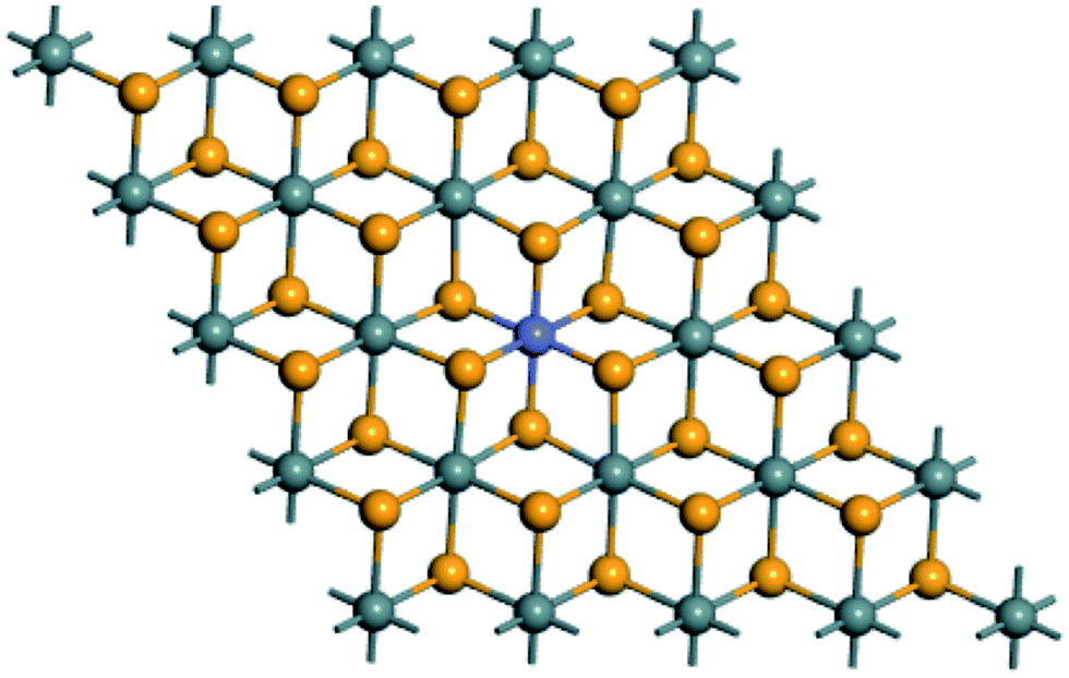 | ||
| Fig. 2 Top view of SnSe2 monolayer doped by one TM atom based on the 4 × 4 × 1 supercell. The grayish, yellow and blue balls represent Sn, Se and TM atoms, respectively. | ||
| Doping | dTM–Se | Mtot | Efor(Sn-rich) | Efor(Se-rich) | ΔE1 | ΔE2 | ΔE3 | TC |
|---|---|---|---|---|---|---|---|---|
| V | 2.546 | 1.00 | −0.19 | −1.30 | 50 | 34 | 21 | 193 |
| Cr | 2.618 | 2.55 | −0.12 | −1.23 | 121 | 31 | 24 | 468 |
| Mn | 2.733 | 3.00 | 0.55 | −0.56 | 37 | 3 | 1 | 143 |
| Fe | 2.458 | 2.00 | 0.88 | −0.22 | 76 | 26 | 18 | 294 |
| Co | 2.424 | 0.83 | 0.94 | −0.17 | 59 | 14 | 2 | 228 |
| Ni | 2.457 | 0 | 0.71 | −0.40 | 0 | 0 | 0 | — |
| Cu | 2.539 | 1.00 | 2.27 | 1.15 | −53 | −4 | −2 | — |
3. Results and discussion
3.1. Structural stability and magnetic stability
As mentioned above, Mn-doped SnSe2 thin films has been fabricated experimentally,20 and thus it is necessary to explore and compare the structural stability of SnSe2 monolayer doped by different TM atoms. We calculate the formation energy by15,25| ΔEf = E(doped) − E(pristine) − nμTM + nμSn, | (1) |
Stable ferromagnetism of a material is crucial for the spintronic applications, and thus we study the magnetic stability of TM-doped SnSe2 monolayer. We need compare the ferromagnetic (FM) and antiferromagnetic (AFM) interactions, and thus two Sn atoms are replaced by two same TM atoms in the 4 × 4 × 1 supercell of SnSe2 monolayer. The FM and AFM configurations are set by the parallel and antiparallel spin orientations between the two TM atoms, respectively. Usually, magnetic interactions between two TM dopants will change with the change of TM–TM distance. Here, we consider two nearest neighboring, next-nearest neighboring and third-nearest neighboring TM atoms. Table 1 lists the calculated total energy difference between the AFM and FM states. It shows that the Ni-doped system is nonmagnetic independent of the Ni–Ni distance. The Cu-doped system has a short-range AFM ground state. All the V-, Cr-, Mn, Fe- and Co-doped systems have lower FM total energies than the AFM states. The FM order is long-range for all the V, Cr and Fe dopants, but it is short-range for the Mn dopants. We also note that the total energy differences between AFM and FM states under nearest neighboring sites are considerable (from 37 to 121 meV per supercell), which mean these V-, Cr-, Mn-, Fe- and Co-doped systems should have high-temperature ferromagnetism. In fact, FM behavior above room temperature has been realized in the recent experiment of Mn-doped SnSe2 thin films.20
3.2. Electronic structure and magnetism
In order to search for possible half-metals and HSCs, we show in Fig. 3(a)–(g) the calculated spin-resolved band structure of SnSe2 monolayer doped by one TM atom within GGA–PBE. For comparison, the electronic band structure of pristine SnSe2 monolayer is also presented. As shown in Fig. 1(h), pristine SnSe2 monolayer is a nonmagnetic semiconductor, and the calculated indirect gap (Γ − M) of 0.85 eV is in agreement with the previous value of 0.80 eV.26 The indirect gap of SnSe2 monolayer is larger than that of SnSe2 bulk (0.71 eV).27 The valence bands around the Fermi level are mainly composed of hybridized Se p electrons with Sn p electrons, and the conduction bands around the Fermi level mainly originate from the hybridized Sn s electrons with Se p electrons. For the doped systems, both V- and Cu-doped SnSe2 monolayers exhibit a HM characteristic, because the spin-up electrons cross the Fermi level, indicating metallicity, while the spin-down band structure is semiconducting. Ni-doped SnSe2 monolayer is a nonmagnetic semiconductor, and both Cr- and Co-doped SnSe2 monolayers are usual magnetic semiconductors. Interestingly, both Mn- and Fe-doped SnSe2 monolayers are HSCs, because both conduction band and valence band are spin split, and the conduction band minimum and valence band maximum possess the same spin down channel. We note that the calculated integer magnetic moments shown in Table 1 also reflect the characteristics of half-metals for both V- and Cu-doped SnSe2 monolayers and HSCs for both Mn- and Fe-doped SnSe2 monolayers. The magnetic moments are mainly from the TM atoms and the nearest neighboring Se atoms.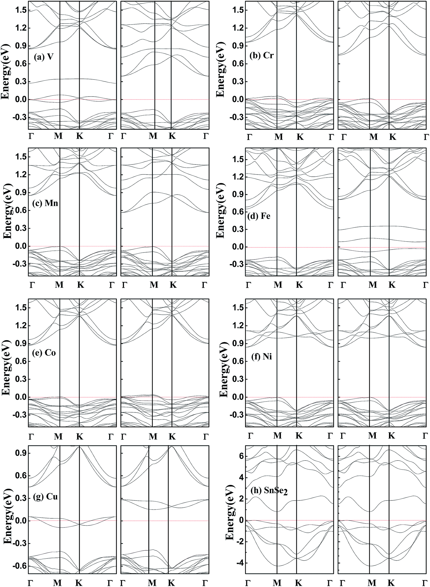 | ||
| Fig. 3 Calculated spin-resolved band structures within GGA–PBE. (a–g) SnSe2 monolayer doped by one V, Cr, Mn, Fe, Co, Ni and Cu atom, respectively. (h) Pristine SnSe2 monolayer. The red dashed line represents the Fermi level at zero eV. | ||
Here, we mainly focus on the doped systems with complete spin polarization, i.e., the half-metals of V- and Cu-doped SnSe2 monolayer and the HSCs of Mn- and Fe-doped SnSe2 monolayer. In order to better understand the electronic structure and magnetism, we present in Fig. 4 the calculated total and main partial density of states (DOS) within GGA–PBE for SnSe2 monolayer doped with V and Mn as the examples of half-metals and HSCs, respectively. The total DOSs around the Fermi level are mainly from the TM 3d electrons and the nearest neighboring Se 4p electrons. One can see from Fig. 4 that there is a large exchange splitting for 3d electrons of V and Mn, providing the main spin magnetic moments in the doped systems. There are obvious orbital hybridization between TM 3d electrons and Se 4p electrons, which induces small magnetic moment in nearest neighboring Se atoms. Under the crystal field of CdI2-type structure, the V (Mn) 3d orbitals are split into a single a (dz2), twofold degenerate e1 (dxy, dx2−y2) and twofold degenerate e2 (dxz, dyz) states. For the case of V-doped system, one know from Fig. 4(a) and 3(a) that one 3d electron in V4+ (3d1) occupies partially the spin-up twofold degenerate e1 states, exhibiting metallicity, while the spin-down 3d states are almost empty, showing semiconductivity, and thus the V-doped system is a HM ferromagnet with the net spin magnetic moment of one μB. The twofold degenerate e2 states mainly take part in the orbital hybridization between V 3d electrons and Se 4p electrons. Similarly, for the case of Mn-doped system, as shown in Fig. 4(b), both spin-up and spin-down electrons show a semiconductor characteristic, because three 3d electrons in Mn4+ (3d3) occupy fully the spin-up twofold degenerate e1 states and the spin-up single a state, and the spin-down 3d states are almost empty. The large exchange split of e2 states makes the energy of the bottom of spin-up e2 states is higher than that of the top of spin-down e1 states, inducing the characteristic of a HSC in Mn-doped SnSe2 monolayer. In addition, only the Ni-doped SnSe2 monolayer is a nonmagnetic semiconductor in all the doped systems studied, which is not difficult to understand, because both spin-up and spin-down twofold degenerate e1 states and single a state are fully occupied by six 3d electrons in Ni4+ (3d6), inducing zero magnetic moment.
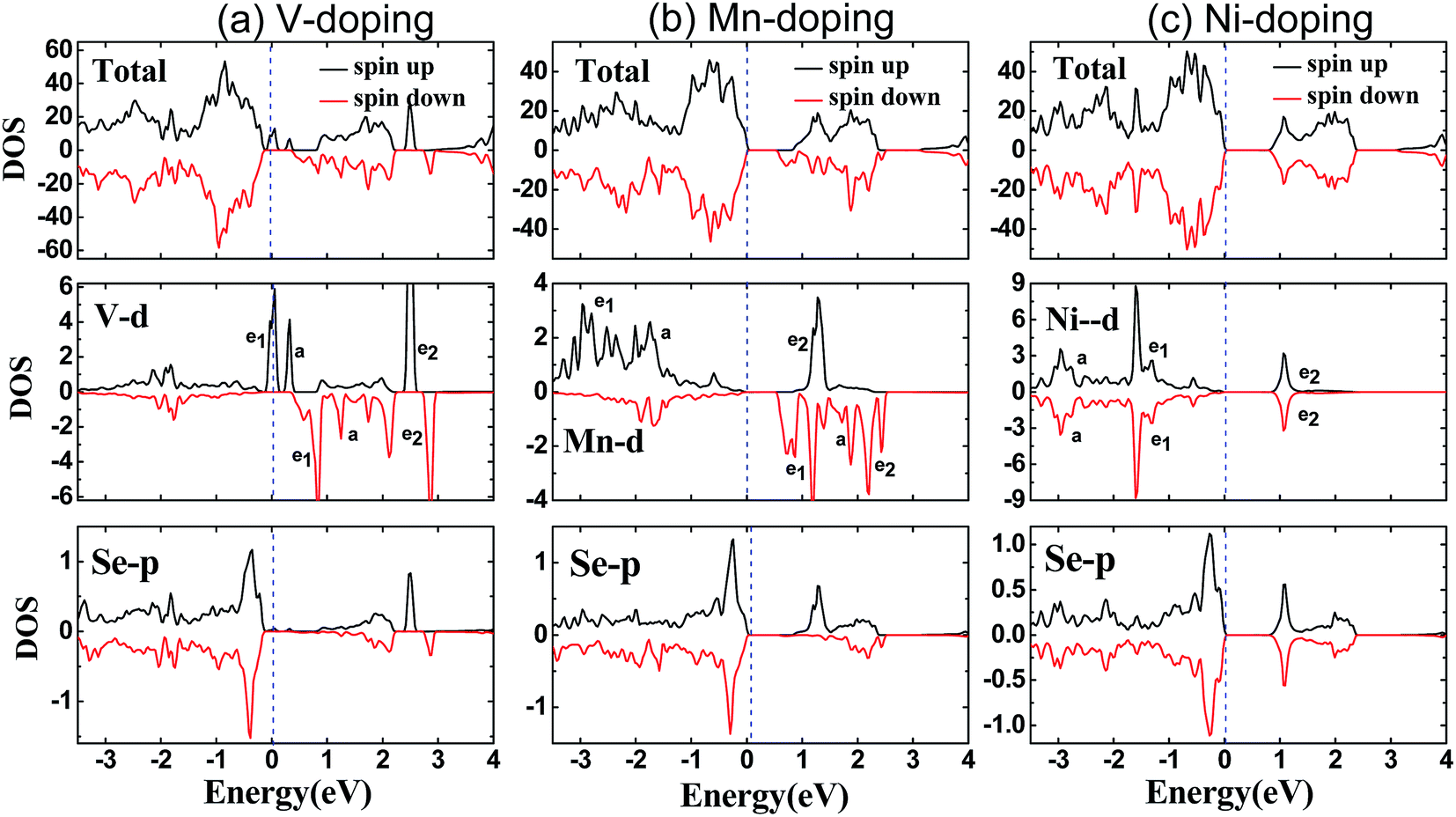 | ||
| Fig. 4 Calculated spin-resolved total and main partial density of states of 3d states of TM atoms and 4p states of nearest neighboring Se atoms in SnSe2 monolayer doped by one V (a), Mn (b), and Ni (c) atom within GGA–PBE. The dashed line represents the Fermi level at zero eV. | ||
Using the relation 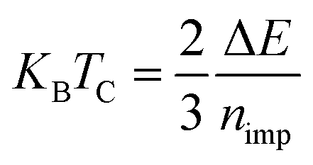 based on the classical Heisenberg model and the mean-field approximation (MFA),28 we estimate the Curie temperature TC, where ΔE is the total energy difference between AFM and FM states under nearest neighboring sites for the 4 × 4 × 1 supercell of doped SnSe2 monolayer (see Table 1), and nimp is the number of TM atoms in the supercell. This method has been extensively used to estimate the Curie temperatures for some TM-doped 2D semiconductors such as phosphorene, germanane, and MoS2.29–31 The estimated Curie temperatures are listed in Table 1. One can see that the values are high especially for the Cr- and Fe-doped systems, which makes them promising candidates for 2D spintronic applications. We note that our estimated Curie temperatures of doped SnSe2 monolayers are higher than those of doped MoS2 monolayers.31 In addition, the estimated Curie temperature of Mn-doped SnSe2 monolayer is lower than the experimental value (above room temperature).20 The reason may be the different Mn doping concentration and the different thickness of SnSe2 thin films. The Mn doping concentration in experiment is much higher than that in our present theory, and the experimental doped SnSe2 thin films is thicker than the doped SnSe2 monolayer we studied. So, it is meaningful to explore the Curie temperatures dependent of the doping concentration and the thickness of SnSe2 films in future works.
Finally, it should be pointed out that above band structures are based on the GGA–PBE for the electronic exchange–correlation functional, and band structures may be different within different functionals. Hybrid functional HSE can usually increase the energy gap of a semiconductor compared to GGA, but the semiconductor property can not be destroyed.24 Considering that all the doped systems studied are semiconductors except for V- and Cu-doped SnSe2 monolayers which are half-metals within GGA-PBE, we perform spin-resolved band structure calculations for V- and Cu-doped SnSe2 monolayers within HSE. As shown in Fig. 5, Cu-doped SnSe2 monolayer is still a half-metal. Although V-doped SnSe2 monolayer is not a half-metal, it becomes a HSC, and the spin polarization is still complete. Comparing Fig. 5(a) with Fig. 3(a), it is clear that, for both spin-up and spin-down channels of V-doped SnSe2 monolayer, the valence bands within HSE move toward the Fermi level compared to those within GGA–PBE, while the conduction bands shift to high energy range (depart from the Fermi level). The spin split becomes weak within HSE compared to GGA–PBE. In addition, we check the effect of spin–orbit coupling (SOC) on the band structures of V- and Cu-doped SnSe2 monolayers. The calculated band structures within SOC shown in Fig. 6 indicate that V-doped SnSe2 monolayer is no longer a half-metal, and it is a HSC with a very small energy gap in the spin-up channel. Half-metallicity is still observed in Cu-doped SnSe2 monolayer. So, no matter GGA, HSE or SOC, both V- and Cu-doped SnSe2 monolayers are high spin-polarized materials.
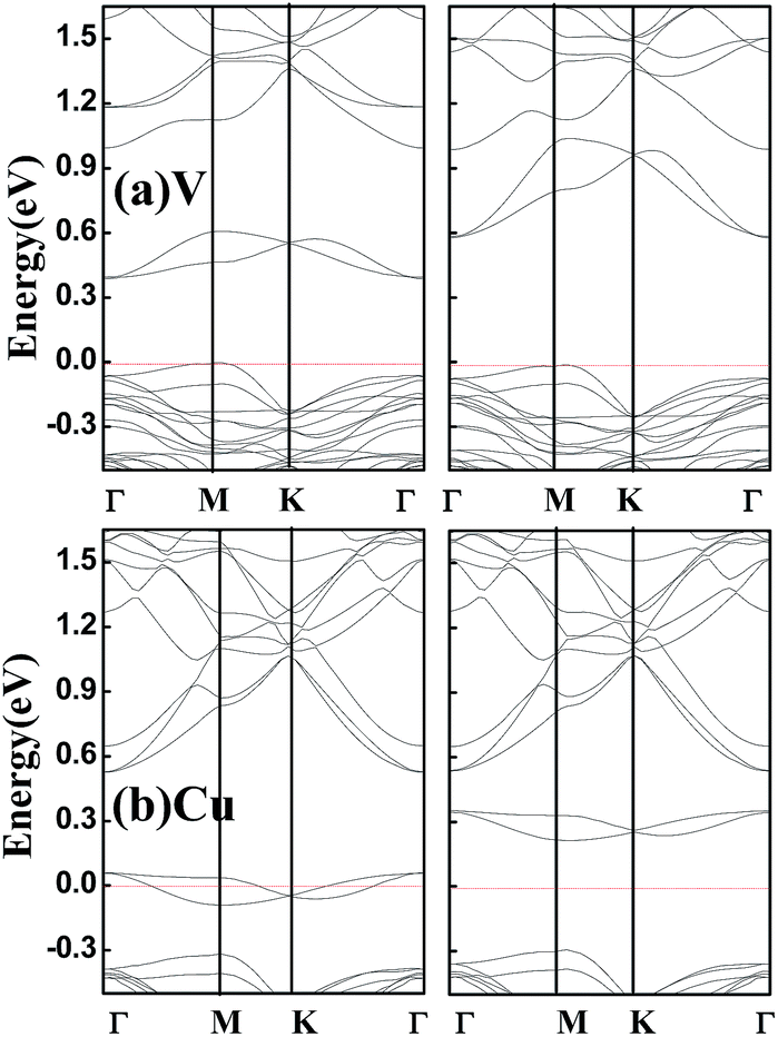 | ||
| Fig. 5 Calculated spin-resolved band structures within HSE for SnSe2 monolayer doped by V (a) and Cu (b). The red dashed line represents the Fermi level at zero eV. | ||
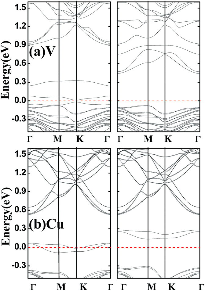 | ||
| Fig. 6 Calculated spin-resolved band structures within GGA–PBE and SOC for SnSe2 monolayer doped by V (a) and Cu (b). The red dashed line represents the Fermi level at zero eV. | ||
4. Conclusions
We have used the first-principles full-potential linearized augmented plane-wave method to explore the structural, electronic and magnetic properties of V-, Cr-, Mn-, Fe-, Co-, Ni- and Cu-doped SnSe2 monolayer. We show from the calculated formation energy that it is easier for substituted doping of SnSe2 monolayer under Se-rich condition except for Cu doping. All the V-, Cr-, Mn-, Fe-, and Co-doped systems have a ferromagnetic ground state, and the Cu-doped system is most stable in antiferromagnetic state, while the Ni-doped system is nonmagnetic. Ferromagnetic orders of V, Cr and Fe dopants are long-range, but it is short-range for ferromagnetic Mn dopants and for antiferromagnetic Cu dopants. Within GGA–PBE, we predict the HM ferromagnetism in V-doped SnSe2 monolayer with 1.00 μB per supercell, and metastable ferromagnetic Cu-doped SnSe2 monolayer also exhibits half-metallicity. Half-semiconductors are found in doping of Mn and Fe with the magnetic moments of 3.00 and 2.00 μB per supercell, respectively. Within HSE or SOC, Cu-doped SnSe2 monolayer is still a half-metal, while V-doped SnSe2 monolayer becomes a HSC. Based on the classical Heisenberg model and the mean-field approximation, the estimated curie temperatures of TM-doped SnSe2 monolayers are high, which make them promising candidates for 2D spintronic applications.Conflicts of interest
There are no conflicts to declare.Acknowledgements
This work was supported by the National Natural Science Foundation of China under Grant No. 11474113, by the Natural Science Foundation of Hubei Province under Grant No. 2015CFB419, and by the Fundamental Research Funds for the Central Universities under Grant No. HUST: 2015TS019.References
- R. A. de Groot, F. M. Mueller, P. G. van Engen and K. H. J. Buschow, Phys. Rev. Lett., 1983, 50, 2024–2027 CrossRef CAS.
- I. Zutic, J. Fabian and S. S. Sarma, Rev. Mod. Phys., 2004, 76, 323–410 CrossRef CAS.
- C. Felser, G. H. Fecher and B. Balke, Angew. Chem., Int. Ed., 2007, 46, 668–699 CrossRef CAS PubMed.
- S. Skaftouros, K. Ozdogan, E. Sasiogl and I. Galanakis, Phys. Rev. B: Condens. Matter Mater. Phys., 2013, 87, 024420 CrossRef.
- X. Wang, Z. Cheng, J. Wang, L. Wang, Z. Yu, C. Fang, J. Yang and G. Liu, RSC Adv., 2016, 6, 57041–57047 RSC.
- X. Li and J. Yang, Natl. Sci. Rev., 2016, 3, 365–381 CrossRef.
- E. Torun, H. Sahin, S. K. Singh and F. M. Peeters, Appl. Phys. Lett., 2015, 106, 192404 CrossRef.
- G. Gao, G. Ding, J. Li, K. Yao, M. Wu and M. Qian, Nanoscale, 2016, 8, 8986–8994 RSC.
- M. Mushtag, Y. Zhou and X. Xiang, RSC Adv., 2017, 7, 22541–22547 RSC.
- W. Zhang, Q. Qu, P. Zhu and C. Lam, J. Mater. Chem. C, 2015, 3, 12457–12468 RSC.
- Z.-K. Tang, W.-W. Liu, D.-Y. Zhang, W.-M. Lau and L.-M. Liu, RSC Adv., 2015, 5, 77154–77158 RSC.
- I. Khan and J. Hong, Nanotechnology, 2016, 27, 385701 CrossRef PubMed.
- Z. Xiang, Z. Zhang, X. Xu, Q. Zhang, Q. Wang and C. Yuan, Phys. Chem. Chem. Phys., 2015, 17, 15822–15828 RSC.
- B. Xia, Q. Guo, D. Gao, S. Shi and K. Tao, J. Phys. D: Appl. Phys., 2016, 49, 165003 CrossRef.
- X. Zhao, T. Wang, S. Wei, X. Dai and L. Yang, J. Alloys Compd., 2017, 695, 2048–2053 CrossRef CAS.
- T. Wang, Y. Li, C. Xia, X. Zhao, Y. An and X. Dai, J. Mater. Chem. C, 2016, 4, 8111–8120 RSC.
- J. Thakur, M. K. Kashyap, H. S. Saini and A. H. Reshak, J. Alloys Compd., 2015, 649, 1300–1305 CrossRef CAS.
- Y. W. Park, et al., 2D Mater., 2017, 4, 014006 CrossRef.
- T. Pei, L. Bao, G. Wang, R. Ma, H. Yang, J. Li, C. Gu, S. Pantelides, S. Du and H.-J. Gao, Appl. Phys. Lett., 2016, 108, 053506 CrossRef.
- S. Dong, et al., APL Mater., 2016, 4, 032601 CrossRef.
- P. Blaha, K. Schwarz, G. K. H. Madsen, D. Kvasnicka and J. Luitz, Wien2k, improved and updated Unix version of the original copyrighted Wien code, which was published by, Vienna University of Technology, 2002 CrossRef CAS; P. Blaha, K. Schwarz, P. Sorantin and S. B. Trickey, Comput. Phys. Commun., 1990, 59, 399 CrossRef CAS.
- J. P. Perdew, K. Burke and M. Ernzerhof, Phys. Rev. Lett., 1996, 77, 3865 CrossRef CAS PubMed.
- H. Liu and L. L. Y. Chang, J. Alloys Compd., 1992, 185, 183–190 CrossRef CAS.
- G. Li, G. Ding and G. Gao, J. Phys.: Condens. Matter, 2017, 29, 015001 CrossRef PubMed.
- L. Sun, W. Zhou, Y. Liu, D. Yu, Y. Liang and P. Wu, Appl. Surf. Sci., 2016, 389, 484–490 CrossRef CAS.
- S. Lebegue, T. Björkman, M. Klintenberg, R. M. Nieminen and O. Eriksson, Phys. Rev. X, 2013, 3, 031002 Search PubMed.
- B. Sun, Z. Ma, C. He and K. Wu, Phys. Chem. Chem. Phys., 2015, 17, 29844–29853 RSC.
- J. Kudrnovsky, I. Turek, V. Drchal, F. Maca, P. Weinberger and P. Bruno, Phys. Rev. B: Condens. Matter, 2004, 69, 115208 CrossRef.
- L. Seixas, A. Carvalho and A. H. C. Neto, Phys. Rev. B: Condens. Matter, 2015, 91, 155138 CrossRef.
- M. Sun, Q. Ren, Y. Zhao, S. Wang, J. Yu and W. Tang, J. Appl. Phys., 2016, 119, 143904 CrossRef.
- Y. Cheng, Z. Zhu, W. Mi, Z. Guo and U. Schwingenschlogl, Phys. Rev. B: Condens. Matter Mater. Phys., 2013, 87, 100401(R) CrossRef.
| This journal is © The Royal Society of Chemistry 2017 |