
 Open Access Article
 This Open Access Article is licensed under a Creative Commons Attribution-Non Commercial 3.0 Unported Licence
Wearable triboelectric nanogenerator using a plasma-etched PDMS–CNT composite for a physical activity sensor†
Min-Ki Kim ,
Myoung-Soo Kim,
Hong-Bum Kwon,
Sung-Eun Jo and
Yong-Jun Kim*
,
Myoung-Soo Kim,
Hong-Bum Kwon,
Sung-Eun Jo and
Yong-Jun Kim*
School of Mechanical Engineering, Yonsei University, 134 Shinchon-dong, Seodaemun-gu, Seoul 120-749, Republic of Korea. E-mail: yjk@yonsei.ac.kr
First published on 13th October 2017
Abstract
Triboelectric nanogenerators (TENGs) have recently shown promising potential as effective energy harvesters using human motion energy. However, the efficiency of polymer-based flexible TENG must be enhanced for various applications. In this work, we propose a flexible TENG with a fluorocarbon plasma-etched polydimethylsiloxane (PDMS)–carbon nanotube (CNT). The fluorocarbon plasma etching causes not only a chemical modification, but also a physical effect on the morphology of the PDMS–CNT surface to enhance the TENG output performance. The added CNT enhances the mechanical properties, such as durability, of a thin film. The etched PDMS structure and the revealed CNTs increase the charge density on the surface. We confirm the effect of different CNT concentrations doped in PDMS and various etching times. We propose a TENG with 4 wt% CNT, which has been subjected to fluorocarbon etching for 60 s. The TENG exhibits an output voltage of 77.8 V, which is 248.7% and 106.5% higher than that of pure PDMS and un-etched PDMS–CNT, respectively. The 20 mm × 30 mm TENG delivers an output power of 1.98 mW (3.29 W m−2) at a matching resistance of 3 MΩ. The TENG exhibits good stability and superior electrical performance, making it capable of driving both the instantaneous operation of 70 LEDs and the charging of a 0.33 μF capacitor to 6.6 V. Furthermore, this TENG can be used as a self-powered physical activity sensor that measures the amount of human activity through the amount of charge in the capacitor.
1. Introduction
Energy-harvesting techniques have attracted attention as an alternative to supplying power to portable electronics, healthcare devices, and wireless sensor systems.1,2 A number of research studies specifically focussed on harvesting energy from the human body using wearable devices.3–6 The human body is a good source of energy because the energy is easily accessible and semi-permanent. Attributes such as high energy conversion efficiency, flexibility, small volume, and biocompatibility are required for application to the human body. Triboelectric nanogenerators (TENGs) have recently been actively studied to convert human body movements into electric energy.7–9 TENGs have high energy conversion efficiency, low cost, and simple structure. Various approaches, including optimized structure,10–13 surface modifications,14–16 and functional materials,17 were developed to increase the TENG efficiency. These approaches improved the capacities of effective energy harvesters as well as various applications, such as motion sensors,18 pressure sensors,19 tactile sensors,20 and devices for muscle stimulation.21 These studies demonstrated the various possibilities of TENGs using human motion.Polydimethylsiloxane (PDMS), which is one of these triboelectric materials, has the advantages of high flexibility, stretchability, and biocompatibility when used in a wearable energy harvester.12,18,22,23 However, PDMS is not a very efficient triboelectric material. Some studies led to the improvement of the energy conversion efficiency of a PDMS-based TENG by increasing the surface area through nano-structures12,22 and fluorocarbon plasma treatment.21 One efficient method to accomplish this is the addition of carbon nanotubes (CNTs) or graphite particles into PDMS.24,25 CNTs also increase the surface charge density and reduce the effective thickness of the PDMS. However, studies regarding PDMS were limited by the buried CNTs surrounded by the PDMS layer. One study solved this limitation by using aligned carbon nanotubes on the PDMS surface.26 However, the approach used also has the disadvantage of involving a complex fabrication process of growing and transferring CNTs. The transferred CNTs have poor durability caused by friction.
In this study, we designed and fabricated a flexible TENG using PDMS–CNT with nanostructures. The nanostructures were uniformly formed on the surface by dry etching to remove the PDMS. The CNTs buried under the PDMS were exposed to the external environment. In addition, the tetrafluoromethane (CF4) plasma chemically fluorinated the PDMS and the CNT, thereby allowing more charges to be stored on the surface. The TENG maximized the charge density on the polymer surface using the nanostructures. Thus, we were able to develop a high-efficiency energy-harvesting device. The effect of various etching times and CNT concentrations on the TENG performance was investigated. Furthermore, we experimented with a real human body using a wearable prototype. We confirmed that the flexible and effective PDMS–CNT film is applicable for energy harvesting using the human body. This TENG can be used as a self-powered physical activity sensor that measures the amount of human activity through the amount of charge in the capacitor.
2. Experimental section
Design of the TENG
Fig. 1(a) shows the schematic diagram of the proposed PDMS–CNT-based TENG. Contact and separation occurred between the surfaces of the PDMS–CNT film and the aluminum (Al) foil when the upper part of the arc-shaped structure was touched. The nano-level PDMS wire on the PDMS–CNT film surface protruded, and numerous CNTs were embedded. The upper Al foil served as one of the triboelectric layers. Al and PDMS had positive and negative tendencies, respectively, in the electron affinity table (Fig. S1†).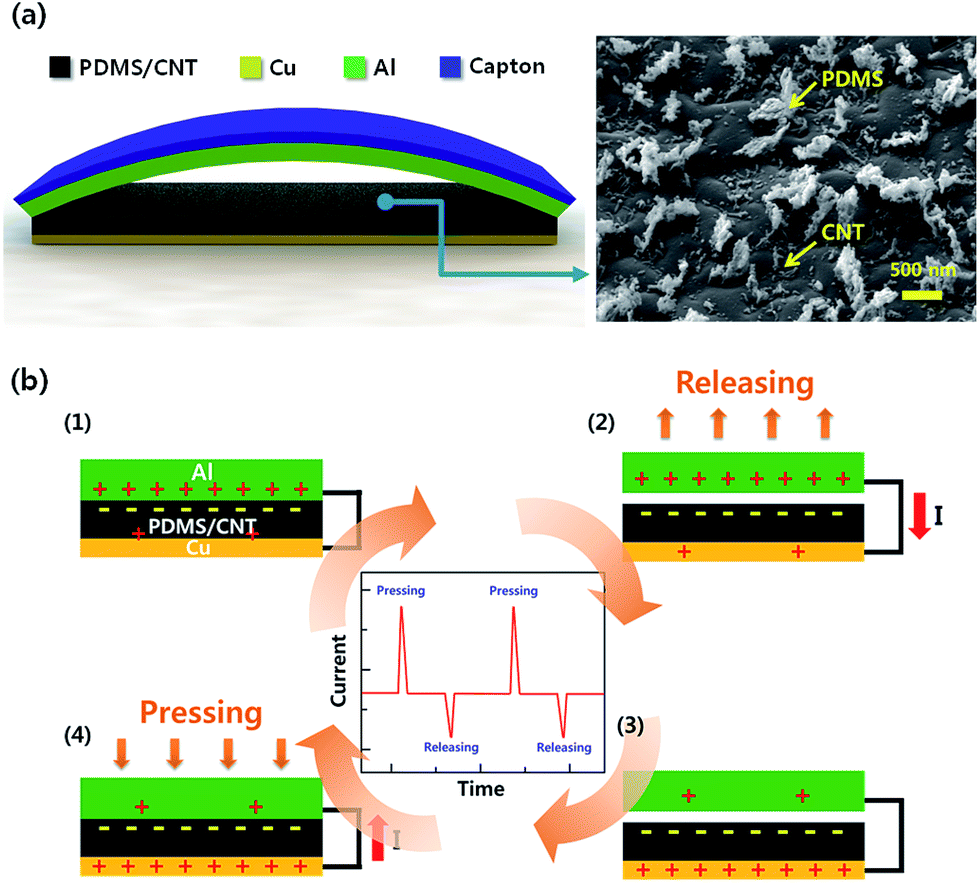 | ||
| Fig. 1 (a) Schematic of proposed flexible triboelectric nanogenerator and FE-SEM image of the PDMS–CNT nanostructures on surface. (b) Working mechanism of the TENG. | ||
The TENG mechanism was based on the coupling of triboelectrification and electrostatic induction. Fig. 1(b) presents the TENG working mechanism. No charge was found on the two material films in the initial state. The upper part was pressed to make contact with the PDMS–CNT. The two different materials then exchanged electrons according to their electron affinities. The PDMS–CNT film that gained electrons became negatively charged, whereas the Al foil that lost electrons became positively charged. The charge on the upper part of the electrode when it separated from the lower part was transferred to the bottom electrode through the external circuit that generated a current. Meanwhile, the charge on the bottom electrode when the upper part was pressed to the PDMS–CNT film transferred to the upper electrode through the external circuit that generated a reverse current. The current disappeared when the electrode reached the bottom position. The cycle was continuously repeated, and current was generated.
Fabrication of the PDMS–CNT composite film
Fig. 2(a) illustrates the TENG fabrication process. The PDMS (Sylgard 184, Dow Corning, USA) and the multi-walled carbon nanotubes (MWCNT) (US Research Nanomaterials, USA) with 20–30 nm outer diameter and 10–30 μm length were used to fabricate the nanocomposites. The CNT was dispersed in chloroform for each concentration through sonication for 3 h, and then mixed with the PDMS base at different concentrations by mechanical stirring for 1 h and further sonication for 3 h at 62 °C to evaporate the chloroform. With almost all the chloroform evaporated, the PDMS curing agent was added at a weight ratio of 1![[thin space (1/6-em)]](https://www.rsc.org/images/entities/char_2009.gif) :10 to the PDMS base. The PDMS mixture with 100 μm thickness was then uniformly spin-coated on a silicon wafer at 1200 rpm for 60 s. Subsequently, the mixture was placed in a vacuum oven for 1 h at 80 °C to degas before allowing to cure at a room temperature for 1 day. The homogeneous distribution of the MWCNTs in the matrix was verified with scanning electron microscopy (SEM) observations. Copper was deposited as an electrode on the fabricated PDMS–CNT film. Oxygen (O2) plasma treatment was then applied for 60 s to increase the adhesive force and the flexible property of the electrode on the polymer. Subsequently, a 500 nm Cu layer was deposited using an E-beam evaporator and the flexible TENG was separated from the glass wafer. The thin film was cut as per experimental size. Fig. 2(b) shows that the PDMS–CNT film can be processed in any shape owing to its stretchability and flexible properties.
:10 to the PDMS base. The PDMS mixture with 100 μm thickness was then uniformly spin-coated on a silicon wafer at 1200 rpm for 60 s. Subsequently, the mixture was placed in a vacuum oven for 1 h at 80 °C to degas before allowing to cure at a room temperature for 1 day. The homogeneous distribution of the MWCNTs in the matrix was verified with scanning electron microscopy (SEM) observations. Copper was deposited as an electrode on the fabricated PDMS–CNT film. Oxygen (O2) plasma treatment was then applied for 60 s to increase the adhesive force and the flexible property of the electrode on the polymer. Subsequently, a 500 nm Cu layer was deposited using an E-beam evaporator and the flexible TENG was separated from the glass wafer. The thin film was cut as per experimental size. Fig. 2(b) shows that the PDMS–CNT film can be processed in any shape owing to its stretchability and flexible properties.
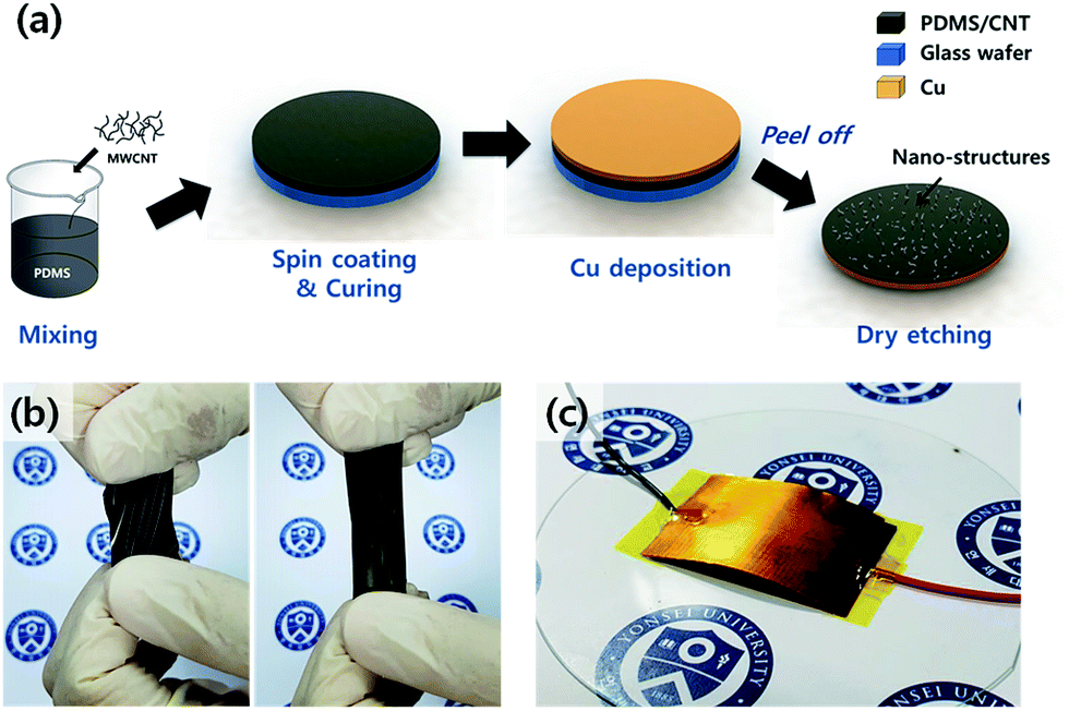 | ||
| Fig. 2 (a) Schematic diagram of the fabrication process using dry etching for PDMS–CNT nanostructures. (b) Photographic images of the stretchable PDMS–CNT film. (c) Photographic image of the fabricated TENG. | ||
Nanostructure fabrication
The opposite side of the PDMS–CNT thin-film electrode was dry-etched using a fluorine-based reactive ion etch (RIE). The RIE process was developed to anisotropically dry etch the silicone elastomer PDMS. Dry etching has a high etch rate for PDMS with a mixture of 25% O2 and 75% CF4.27 However, the dry etching effect on the CNT was relatively small. O2 and CF4 gases were supplied into the RIE chamber at flow rates of 10 and 30 sccm, respectively. The PDMS–CNT film was etched using a 100 W power source to generate high-density plasma, produce the nanostructure, and remove the PDMS. The PDMS bundles remained and became nanostructure pillars. These structures were studied in other studies to improve the TENG.10,12,24 More importantly, the CNT remained to form the nanostructure. The long-exposed CNTs were partially damaged by dry etching and became shorter and thinner. However, the amount of the CNTs relative to the PDMS on the surface increased. Fig. 2(c) illustrates the completion of the TENG fabrication process by using the Al foil on the opposite side and connecting each film by electrodes. The device measured 20 mm × 30 mm, and the maximum arc-shaped gap between the two triboelectric layers was 2 mm.Method of output performance testing
The tapping force exerted by the finger was approximately 5 N, at a constant frequency. The TENG outputs were measured using a multimeter and an oscilloscope (Recroy, 6050A), whereas the current and voltage were measured using a 10 MΩ load resistor. The nanostructure morphology was observed by employing field-mission scanning electron microscopy (FE-SEM, JEOL-7800F) and energy dispersive spectroscopy (EDS).3. Results and discussion
Fig. 3(a)–(d) show the FE-SEM images of the PDMS–CNT nanostructures according to the etching time. The nanostructures on the non-treated PDMS–CNT surface were hardly visible because the CNTs were buried in the PDMS, as shown in Fig. 3(a). Fig. 3(b)–(d) shows the FE-SEM images of a nanostructures on films subjected to different etching time. The nanostructures were clearly visible after dry etching. The nanostructures were stuck out at regular intervals and heights. The aspect ratio of the PDMS structure increased when the etching time increased, as shown in the FE-SEM images of 1000× magnification. The exposed CNT was also visible in the images of 50000× magnification. In the photograph, a part of the CNT is shown on the surface. The total number of CNTs found did not increase even when the etching time was further increased. When etched on for a long time, the CNT was partially destroyed.
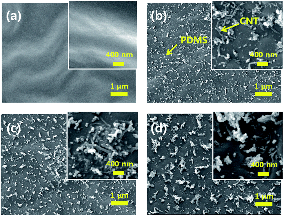 | ||
| Fig. 3 FE-SEM images of the nanostructured PDMS and CNT by etching time of (a) 0 s, (b) 30 s, (c) 60 s, and (d) 90 s (1000× and 50000× of magnifications). | ||
Fig. 4(a) shows the effect of the CNT concentration on the TENG. The highest voltage of the TENG was measured when the CNT concentration was 4 wt%. Meanwhile, an high density composite was observed in the liquid state with extremely high viscosity for CNT concentrations higher than 4 wt%. Therefore, making a thin film by spin-coating was difficult. The experiments were conducted with 4 wt% CNT, which made it easier to produce a thin film with excellent performance.
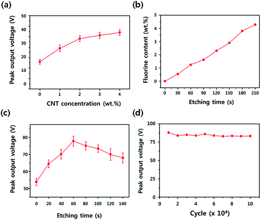 | ||
| Fig. 4 (a) Peak values of output voltage using PDMS–CNT film with CNT contents. (b) EDS results of the fluorine content according to etching time. (c) Peak values of output voltage according to etching time. (d) Change of TENG output performance as the impact time increases. | ||
The PDMS–CNT surface was chemically deformed to deposit the fluorocarbon polymeric layer during the CF4 plasma etching. The CF4 plasma etching led to not only a physical modification to enhance the TENG output performance, but also a chemical effect on the morphology of the surface-textured PDMS film.21 As presented in Fig. 4(b), the EDS analysis showed the deposited fluorocarbon polymeric layer owing to an increase in the fluorine content according to the plasma-etching time. Fig. S3† illustrates the detailed EDS data. The surface became hydrophobic and more resistant to moisture and contamination because of the nanostructures and fluorination. The adhesion between the films did not occur because the specific stickiness of the PDMS was reduced.
Fig. 4(c) shows the peak values of the output voltages according to the etching time. The output voltage constantly increased from 0 s to 60 s. The highest voltage of 77.8 V was obtained with the sample etched for 60 s. From then on, the result was a decrease in output voltage. The PDMS and CNT nanostructures were produced as shown in the photograph. The CNTs exposed by dry etching increased the charge density on the surface and confirmed the performance improvement of the TENG. Excessive exposure time or power increased the amount of CNT destruction and the TENG efficiency was not improved any further. The nanostructures with high aspect ratio could be fabricated when etched for a very long time (Fig. S4†). The voltage did not rise in direct proportion to the depth of the PDMS structure. In addition, the structure size or fluorine content did not seem to have a direct effect on efficiency. The optimal condition was to expose the CNTs and PDMS structures that were not significantly destroyed. Furthermore, the fabricated TENG exhibited excellent stability during repetitive motion. We investigated the stability of the TENG through 105 cycles of tapping. The TENG was attached to the vibration source for the stability test (V4 shaker, Gearing & Watson Electronics Ltd.). Fig. 4(d) shows that the performance remains steady even after repeated experiments. This excellent durability made the TENG advantageous as a sustainable power source.
We compared the power of the PDMS-based TENG without a CNT to investigate the CNT effect. The film thickness, size, and etching conditions were the same. Fig. 5(a) and (b) shows the peak voltages of 26.1 V, 53.9 V, and 91.0 V for the PDMS, un-etched PDMS–CNT, and etched PDMS–CNT, respectively. The output voltage of the fabricated device was 248.7% and 106.5% higher than that of the pure PDMS and the un-etched PDMS–CNT, respectively. We confirmed that a higher efficiency can be obtained by changing the property of the film itself and the surface structure. Furthermore, the PDMS without a CNT was easily torn when made into a thin film. Thin films were difficult to produce, and applications were limited. The internal resistance was lowered even for films of the same thickness because of the CNT conductivity.
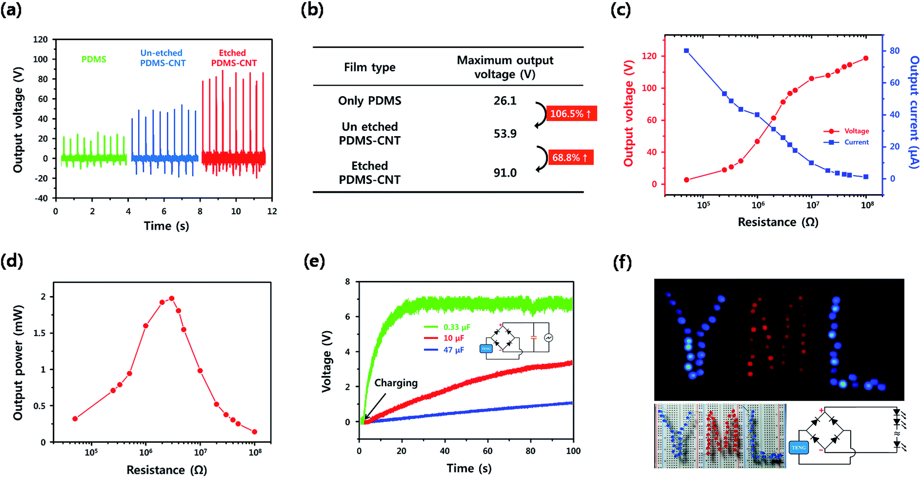 | ||
| Fig. 5 Electrical characteristics of the flexible TENG. (a) Output voltage of the TENG with three-types of films. (b) The maximum output voltage for the each film type. (c) Peak values of output current and voltage using TENG with various load resistances. (d) Output power as a function of load resistance. (e) Charging curves for 0.33 F, 10 F and 47 F capacitors when using fabricated TENG. (f) 70 serially connected LED bulbs. All the electrical characteristics are attained at vertical force of 5 N. | ||
Fig. 5(c) illustrates the closed-circuit voltage and the current for a range of load resistances. Different resistances ranging from 50 kΩ to 100 MΩ were applied to determine the optimized maximum power output. With an increase in the resistance, the voltage increased and the current decreased. Fig. 5(d) presents the generated output power during that time. The maximum power was 1.98 mW (3.29 W m−2) for a load resistance of 3 MΩ. The corresponding output voltage and current were 77 V and 25.7 μA, respectively.
The charging of capacitors with different capacitance values was also experimented herein. A bridge circuit was used to rectify the AC voltage. Fig. 5(e) shows charging with various capacitors (i.e., 0.33, 10, and 47 μF). The 0.33 μF capacitor was charged by the TENG to 6.6 V in 30 s under periodic pressing and releasing. Moreover, the charging was 3.2 V in 100 s for the 10 μF capacitor and 0.99 V in 100 s for the 47 μF capacitor. The produced energy was used to illuminate 70 LEDs (red and blue color) in the dark (Fig. 5(f)). Such electric energy can be used as an energy source for various sensors and small electronic equipment. Capacitors and LEDs are connected in a circuit as shown in the Fig. 5(f).
Self-powered physical activity sensor
Meanwhile, we constructed the wearable form of TENG expected to be attached to one's lap. The arc-shaped TENG functioned with the bending and expanding of the knee. A person wore the wearable prototype of the TENG on his lap and walked at a constant speed for the self-powered physical activity sensor test (Fig. 6(a)). The device was fixed on the knee, and the storage circuits were placed inside the fabric. Frictional energy was harvested by the contact that occurred when the knee bended while walking or running. As shown in Fig. 6(b), the speed at which the capacitor is charged varies with the walking speed. When the subject moved at a velocity of 0.8, 1.5, and 3.0 m s−1, the 100 μF capacitor was charged at a slope of 0.96, 1.70 and 3.65 mV min−1. This device can be a self-powered sensor that can be used for monitoring the amount of activity. The amount of energy accumulated in the capacitor linearly increased with the amount of motion. A 100 μF capacitor was charged to 113.4 mV over a 30 min walk. This linear increase can infer the amount of movement of the person as well as the energy storage. The slope of the charging voltage depended on the speed of each movement. The caloric costs of walking and running were 0.47 kcal kg−1 km−1 and 0.89 kcal kg−1 km−1 for a 75 kg man.28 The energy was stored as shown in Fig. 6(c) while the male subject was exercising for 30 min. The graph shows that the slope to be charged differs each time you walk, run or stop. A total of 119.27 kcal was estimated to be consumed. Furthermore, the energy collected over a long duration can be used as the power source for another sensor being used for health care.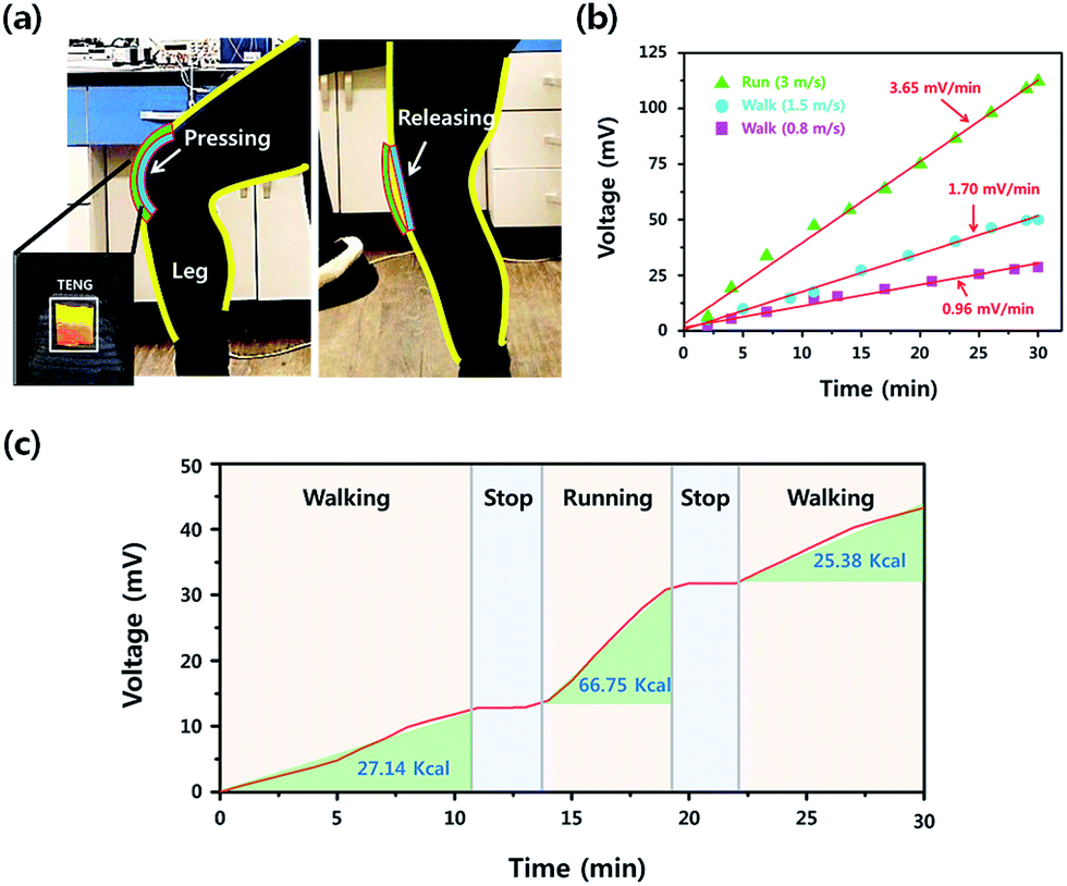 | ||
| Fig. 6 (a) Photographs of the pair of pants with the TENG embedded for clothing applications. (b) Charging voltage of 100 μF capacitor according to the walking and running speed. (c) Charging voltage corresponding to the motion of a 75 kg man for 30 min. | ||
4. Conclusions
In this study, we proposed a high-performance PDMS–CNT composite-based flexible TENG. The CNT in the PDMS enhanced the mechanical and electrical properties of the thin film. Fluorocarbon plasma etching was performed to obtain the PDMS nanostructure and expose the buried CNTs to the surface. Furthermore, the PDMS and the CNT were chemically fluorinated on the film. These effects increased the charge density. A more robust and enhanced performance also increased the potential of the device to be used as a wearable TENG. Several samples were fabricated to demonstrate the effect of concentration and etching time on the device's performance. As a result, the maximum power of the PDMS–CNT-based TENG was generated at 4 wt% of the CNT at an etching time of 60 s. The device, which was fabricated with dimensions of 20 mm × 30 mm, showed an output power of 1.98 mW at a matching resistance of 3 MΩ. The nanogenerator was capable of driving both the lighting of 70 LEDs and the charging of a 0.33 μF capacitor to 6.6 V with its output. Furthermore, we can improve the device by combining with other attractive methods of the improving TENG performance such as reducing the frequency of the charging/discharge process29 or using multilayered-electrode.12,30,31 Our future work will focus on the development of the TENG power density using the above methods. The proposed energy-harvesting device can be applied to the self-powered physical activity sensor. Through this, it is possible to deduce the amount of activity when a person moves. At the same time, electrical energy is harvested by the TENG. We demonstrate the results of the experiment performed with the device attached to the human knee. In conclusion, the enhanced PDMS–CNT-based TENG has a promising potential for stretchable and biocompatible applications in wearable devices.Conflicts of interest
There are no conflict to declare.Acknowledgements
This research was supported by the Pioneer Research Center Program through the National Research Foundation of Korea, funded by the Ministry of Science, ICT & Future Planning (2011-0001672).References
- F. K. Shaikh and S. Zeadally, Renewable Sustainable Energy Rev., 2016, 55, 1041–1054 CrossRef.
- K. V. Selvan and M. S. Mohamed Ali, Renewable Sustainable Energy Rev., 2016, 54, 1035–1047 CrossRef.
- W. Zeng, L. Shu, Q. Li, S. Chen, F. Wang and X. M. Tao, Adv. Mater., 2014, 26, 5310–5336 CrossRef CAS PubMed.
- F. Suarez, A. Nozariasbmarz, D. Vashaee and M. C. Öztürk, Energy Environ. Sci., 2016, 9, 2099–2113 CAS.
- M.-K. Kim, M.-S. Kim, S. Lee, C. Kim and Y.-J. Kim, Smart Mater. Struct., 2014, 23, 105002 CrossRef.
- F. R. Fan, W. Tang and Z. L. Wang, Adv. Mater., 2016, 28, 4283–4305 CrossRef CAS PubMed.
- X.-S. Zhang, M.-D. Han, B. Meng and H.-X. Zhang, Nano Energy, 2015, 11, 304–322 CrossRef CAS.
- Z. L. Wang, ACS Nano, 2013, 7, 9533–9557 CrossRef CAS PubMed.
- Z. L. Wang, J. Chen and L. Lin, Energy Environ. Sci., 2015, 8, 2250–2282 CAS.
- W. Du, X. Han, L. Lin, M. Chen, X. Li, C. Pan and Z. L. Wang, Adv. Energy Mater., 2014, 4, 1301591 Search PubMed.
- H. Guo, Q. Leng, X. He, M. Wang, J. Chen, C. Hu and Y. Xi, Adv. Energy Mater., 2015, 5, 1400790 CrossRef.
- Y. Kang, B. Wang, S. Dai, G. Liu, Y. Pu and C. Hu, ACS Appl. Mater. Interfaces, 2015, 7, 20469–20476 CAS.
- W. Tang, B. Meng and H. Zhang, Nano Energy, 2013, 2, 1164–1171 CrossRef CAS.
- B. Dudem, Y. H. Ko, J. W. Leem, S. H. Lee and J. S. Yu, ACS Appl. Mater. Interfaces, 2015, 7, 20520–20529 CAS.
- D. Kim, S.-B. Jeon, J. Y. Kim, M.-L. Seol, S. O. Kim and Y.-K. Choi, Nano Energy, 2015, 12, 331–338 CrossRef CAS.
- W. Shang, G. Q. Gu, F. Yang, L. Zhao, G. Cheng, Z.-l. Du and Z. L. Wang, ACS Nano, 2017, 11, 8796–8803 CrossRef CAS PubMed.
- Z.-H. Lin, Y. Xie, Y. Yang, S. Wang, G. Zhu and Z. L. Wang, ACS Nano, 2013, 7, 4554–4560 CrossRef CAS PubMed.
- L. Dhakar, P. Pitchappa, F. E. H. Tay and C. Lee, Nano Energy, 2016, 19, 532–540 CrossRef CAS.
- F. R. Fan, L. Lin, G. Zhu, W. Wu, R. Zhang and Z. L. Wang, Nano Lett., 2012, 12, 3109–3114 CrossRef CAS PubMed.
- X. Z. Jiang, Y. J. Sun, Z. Fan and T. Y. Zhang, ACS Nano, 2016, 10, 7696–7704 CrossRef CAS PubMed.
- X.-S. Zhang, M.-D. Han, R.-X. Wang, B. Meng, F.-Y. Zhu, X.-M. Sun, W. Hu, W. Wang, Z.-H. Li and H.-X. Zhang, Nano Energy, 2014, 4, 123–131 CrossRef CAS.
- Y. H. Ko, G. Nagaraju, S. H. Lee and J. S. Yu, ACS Appl. Mater. Interfaces, 2014, 6, 6631–6637 CAS.
- G. Zhu, Z. H. Lin, Q. Jing, P. Bai, C. Pan, Y. Yang, Y. Zhou and Z. L. Wang, Nano Lett., 2013, 13, 847–853 CrossRef CAS PubMed.
- Y. Zhu, B. Yang, J. Liu, X. Wang, L. Wang, X. Chen and C. Yang, Sci. Rep., 2016, 6, 22233 CrossRef CAS PubMed.
- X. He, H. Guo, X. Yue, J. Gao, Y. Xi and C. Hu, Nanoscale, 2015, 7, 1896–1903 RSC.
- H. Wang, M. Shi, K. Zhu, Z. Su, X. Cheng, Y. Song, X. Chen, Z. Liao, M. Zhang and H. Zhang, Nanoscale, 2016, 8, 18489–18494 RSC.
- J. Garra, T. Long, J. Currie, T. Schneider, R. White and M. Paranjape, J. Vac. Sci. Technol., A, 2002, 20, 975–982 CAS.
- E. T. Howley and M. E. Glover, Med. Sci. Sports, 1974, 6, 235–237 CAS.
- G. Cheng, Z.-H. Lin, L. Lin, Z.-l. Du and Z. L. Wang, ACS Nano, 2013, 7, 7383–7391 CrossRef CAS PubMed.
- G. Cheng, L. Zheng, Z. H. Lin, J. Yang, Z. Du and Z. L. Wang, Adv. Energy Mater., 2015, 5, 1401452 CrossRef.
- G. Cheng, Z. H. Lin, Z. Du and Z. L. Wang, Adv. Funct. Mater., 2014, 24, 2892–2898 CrossRef CAS.
Footnote |
| † Electronic supplementary information (ESI) available. See DOI: 10.1039/c7ra07623a |
| This journal is © The Royal Society of Chemistry 2017 |