
 Open Access Article
 This Open Access Article is licensed under a Creative Commons Attribution-Non Commercial 3.0 Unported Licence
Coulomb explosion of vertically aligned carbon nanofibre induced by field electron emission†
Yunhan Lia,
Yonghai Sunb,
David A. Jaffrayb and
John T. W. Yeow *a
*a
aDepartment of Systems Design Engineering, University of Waterloo, 200 University Ave. West, Waterloo, Ontario, Canada N2L 3G1. E-mail: jyeow@uwaterloo.ca
bPrincess Margaret Cancer Centre, 610 University Ave, Toronto, ON, Canada M5G 2M9
First published on 21st August 2017
Abstract
Carbon nanofibre (CNF) field emitter failure is often encountered but there is a lack of understanding of its degradation behaviour and mechanism. This study, starting with a direct observation of a light emission followed by an Coulomb explosion, presents a systematic characterization of CNF emitter failure using a PMMA (poly(methyl methacrylate)) thin film based field emission microscopy (FEM) method. This unique CNF emitter failure behaviour is due to a combined effect of Joule heating and excessive charging at high FE current, ranging from 1.95 μA to 41.82 μA. Joule heating converts FE to extended Schottky emission and heats CNFs almost instantaneously. With the aid of Joule heating, Coulomb explosions disintegrate CNFs and generate annular craters of 60–70 μm on the PMMA thin film, melted areas of 10–20 μm on the substrate, and a sputter of PMMA around the emission sites in a range of 100–120 μm. This study successfully explains the behaviour and mechanism of CNF absence after FE, which is often simply attributed to uprooting or burnout of the CNFs. The detailed study of Coulomb explosion of CNF induced by FE allows the systematic design and optimization of CNF FE devices for long-lasting operation.
1. Introduction
There has been a keen interest in the application of vertically aligned carbon nanofibres (CNF) as field electron sources in various applications such as field emission display, microwave amplifier, parallel electron beam lithography, and multi-beam X-ray sources.1–6 Benefiting from the well-controlled geometry and a large number of exposed tips, CNF field emitters have a higher field emission (FE) efficiency and performance compared with single-walled carbon nanotubes (SWNT) and multi-walled carbon nanotubes (MWNT).2,7–10 Vertically aligned CNF is fabricated by plasma-enhanced chemical vapor deposition (PECVD) with acetylene and ammonia at 700 °C at precisely positioned nickel (Ni) catalyst dots.11–14 Each site has a single vertically aligned CNF emitter with stacked curved graphite layers that form a tubular conical structure.15,16 One of the limitations for CNF FE is the irreversible damage of dominating CNF emitters at high FE current leading to unstable and non-uniform FE performance. However, the behaviour and mechanism of vertically aligned CNF field emitter failure induced by FE is still insufficiently studied, which is often simply attributed to uprooting or burnout of CNF emitters.4,17,18 Most investigation reported previously are the failure of SWNTs and MWNTs such as peeling or splitting of the outer shells of MWNTs and removal of cap of SWNTs and MWNTs.19–23 These studies are performed using techniques such as field emission microscopy (FEM) based on fluorescent effect, in situ scanning electron microscopy (SEM), in situ transmission electron microscopy (TEM) to study structure change after certain FE conditions.19,22–25 In contrast to this structure change induced by FE, abrupt failure of the emitter is difficult to capture and observe. Thus, further characterization of the abrupt nanotube destruction and understanding of the mechanism are limited.These issues can be resolved by our previously proposed FEM method based on poly(methyl methacrylate) (PMMA) thin film with a microscopic camera.26 The high sensitivity to low energy electrons of PMMA thin film is able to record the FE performance of each CNF emitter from a CNF field emitter arrays (FEA). The transparency of PMMA thin film allows direct observation of the process and history of CNF emitter failure induced by FE. Using this method, we are able to observe CNF emitter failure process, which exhibits a light emission followed by an explosion.26 However, the mechanism behind this phenomenon demands further characterization and understanding.
Explosions found in various types of charged clusters exploding into smaller fragments are called Coulomb explosion.27–33 Apart from some Coulomb explosions induced by chemical reaction,33 X-ray,34 and electron beam irradiation,30 most Coulomb explosions reported are induced by laser pulse excitation.27–29 Herein, we report a comprehensive investigation of the unique phenomenon of light emission and Coulomb explosion of vertically aligned CNF induced by FE for the first time. In the study, starting with the direct observation of the unique behaviour by a microscopic video camera, a systematic characterization of the CNF emitter failure process using the PMMA thin film based FEM method combined with various techniques is performed. Finite element analysis and theoretical study are carried out to explore the effect of Joule heating on the FE and the CNF explosion. The Coulomb explosion of CNF, a combined effect of Joule heating and excessive charging, is characterized by the size and shape of the explosion impacts on the PMMA thin film, sputtered PMMA by charged fragments, and the melted area in the explosion centres. This study represents the entire process of the light emission and Coulomb explosion of CNF induced by FE and provides a deep understanding of its mechanism.
2. Experimental
2.1 Vertically aligned CNF FEA synthesis
Two aspects are considered to design the CNF FEA for this study: inter-emitter distance must be large enough to avoid neighbouring emitter explosion interaction and the number of CNF field emitter in an array should be large enough to show the generality. The designed vertically aligned CNF FEA is an 11 × 11 array with an inter-emitter distance of 100 μm in a square of 1 mm2. The CNF FEA is patterned on a titanium nitride (TiN) layer (70 nm) on a silicon substrate. The CNF is synthesized in a PECVD system (Black Magic, Aixtron, Germany) at 700 °C and 5.5 mbar for 10 minutes in acetylene (C2H2, 50 sccm) and ammonia (NH3, 200 sccm) gases atmosphere. The CNF emitters has an average height of 5.12 μm and a standard deviation of 0.55 μm, corresponding to 10.7% of the average (ESI†). This data is in good agreement with that reported in the previous study (6.3%).132.2 Emitter failure experiment
In the experiment, a PMMA 950K A3 thin film layer is spin coated on a piece of indium tin oxide (ITO) coated glass at a spinning speed of 2000 rpm for 45 s to have a thickness of about 210 nm. The transparent ITO glass as the anode allows direct observation of light emission and Coulomb explosion by a video camera with a microscopic lens and a light source. The gap between the anode and the CNF FEA is 25 μm. A picoammeter is used to apply a voltage bias for FE and measure the corresponding FE current from the CNF FEA. The FE experiment is performed at a base pressure of 2 × 10⁻⁸ Torr. In the experiment, the video camera focuses on the PMMA thin film surface. FE current is recorded every 0.5 s by the picoammeter. A bias voltage is applied from 300 V and increased by 50 V to find anything that is recorded by the video camera. Video camera recorded 8 explosions at a voltage of 400 V. Then the voltage is increased to 450 V to observer more explosions. Optical microscopic imaging is used to characterize the FEM patterns and explosion impacts on the PMMA thin film. Scanning electron microscopy (SEM), energy-dispersive X-ray spectroscopy (EDS), and atomic force microscopy (AFM) are used to characterize the CNF emitters and explosions.3. Results
3.1 Direct observation of the light emission and Coulomb explosion of CNF emitters
The direct observation by the microscopic video camera shows that CNF emitter explosion occurs independently in the CNF FEA. Video recording of the light emission and Coulomb explosion are available from ESI videos.† To address any CNF emitter in the array, we number the CNF emitters. The row is numbered alphabetically from bottom to top and the column is numbered numerically from left to right. Fig. 1 shows video recording of the entire process of the light emission and the Coulomb explosion at site A-2 in chronological sequence. First, a small FE exposed spot on the PMMA thin film is seen (Fig. 1(a)). Then, a bright light emission occurs (Fig. 1(b)). Finally, an explosion occurs in the next 27 seconds creating a “firework-like” pattern on the PMMA thin film surface (Fig. 1(c)).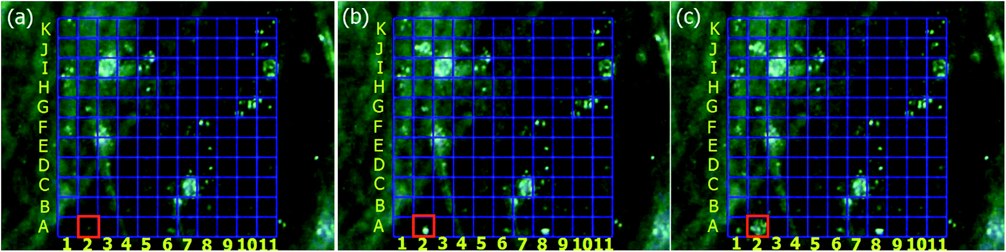 | ||
| Fig. 1 The entire process of the light emission and the Coulomb explosion at the site A-2: (a) a FE spot generated; (b) a light emission occurs; (c) an explosion occurs. | ||
Similar phenomena are observed from other FE sites. The difference is that the light emission duration and intensity varies from emitter to emitter. Fig. 2 presents the entire process of a light emission followed by an explosion from the CNF emitter at site F-5 in chronological sequence captured from video recording. A light emission from the CNF emitter at site F-5 occurs (Fig. 2(b)) and then fades away. A dot is left on the PMMA thin film due to FE exposure (Fig. 2(c)). After 217 seconds, the light emission re-occurs (Fig. 2(d)). In the next 5 seconds, an explosion is observed (Fig. 2(e)).
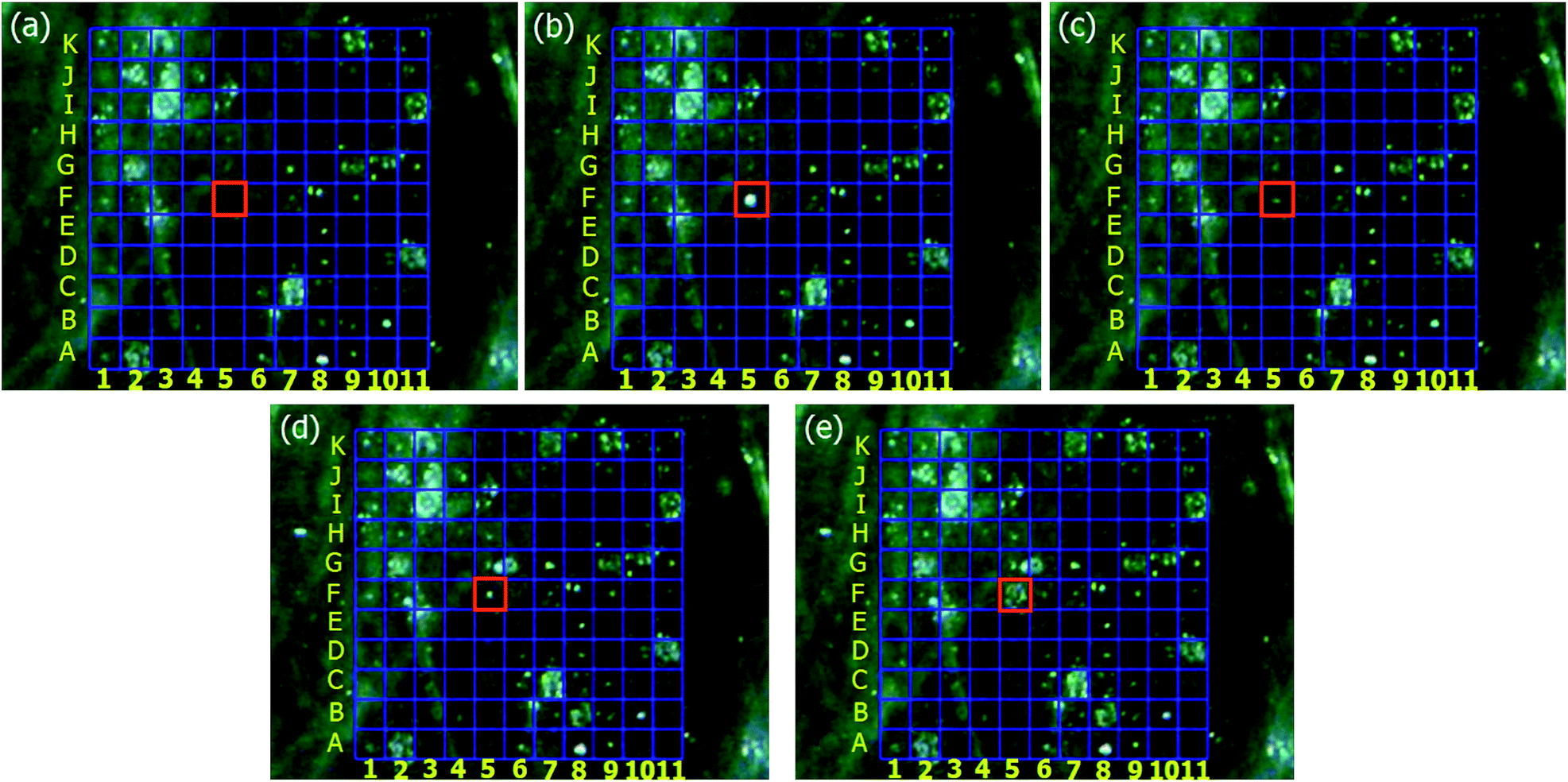 | ||
| Fig. 2 The entire process of a light emission followed by an explosion at the site F-5: (a) nothing; (b) a bright light emission occurs; (c) FE exposed dot is generated; (d) the light emission re-occurs; (e) CNF emitter explosion. | ||
Fig. 3 shows the entire process of the light emission and Coulomb explosion at site G-9. The light emission from the CNF emitter increases from nothing (Fig. 3(a)) to a maximum intensity (Fig. 3(b) and (c)). Then an explosion of the CNF emitter occurs within the next 2 seconds (Fig. 3(d)).
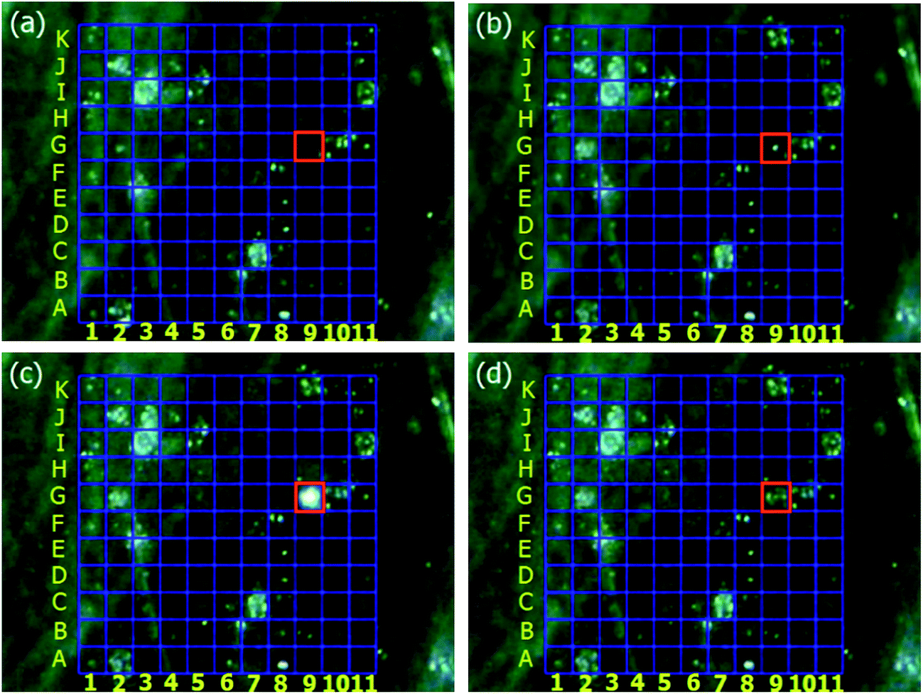 | ||
| Fig. 3 The entire process of the light emission and the Coulomb explosion at the site G-9: (a) nothing; (b) a light emission occurs; (c) a maximum light emission; (d) an explosion occurs. | ||
3.2 Characterization of the light emission and Coulomb explosion of CNF emitters
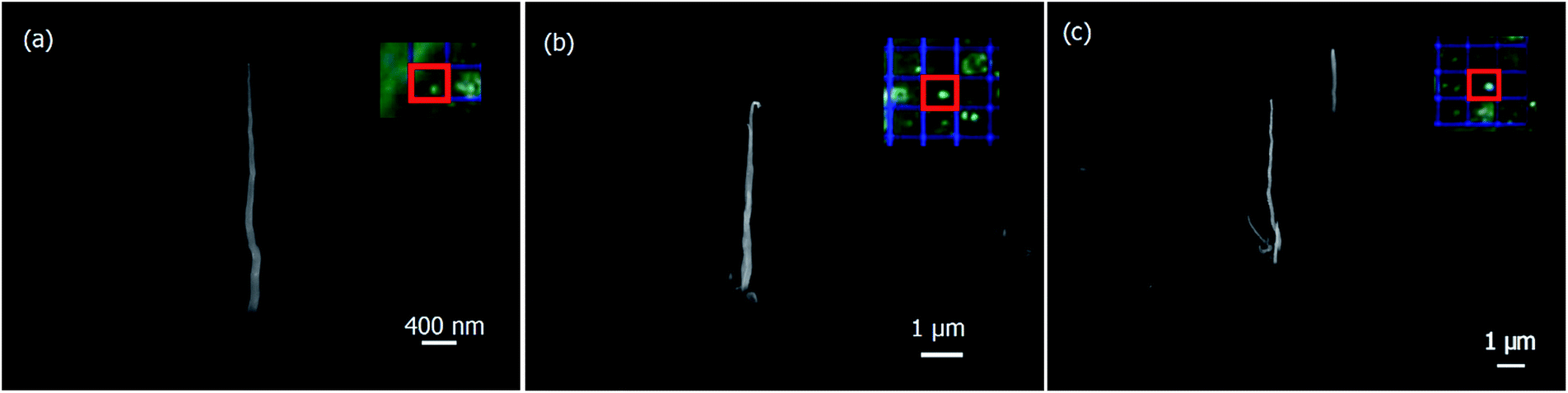
Another FE test is performed using a 10 × 10 CNF FEA under the same conditions except for no PMMA thin film on the ITO coated glass. This experiment confirms that it is the CNF emitters rather than PMMA thin film or other particles that explode. (Detailed experimental validation is available in the ESI†). SEM is used to locate the CNF emitters at site A-2 (Fig. 4(a)), F-5 (Fig. 4(b)), and G-9 (Fig. 4(c)). However, in the place of the emitters, melted substrate and explosion debris are found at the each corresponding site. The melted area in the explosion site has a diameter of 10–20 μm. Fig. 4(d) shows the magnified SEM image of the burnt area in the explosion site at site A-2. The thin TiN layer and silicon substrate are damage showing a history of substrate melt. Silicon is exposed according to EDS analysis (ESI†). The explosion debris points outward in the radial direction from the explosion centre. The debris, considering the experiment set-up and EDS analysis, is believed to be PMMA. The PMMA thin film is blasted away from the anode surface by the CNF emitter explosion. Fig. 4(e) shows four neighbouring emission sites after the experiment: B-6, B-7, C-6, and C-7 from the lower left to the upper right. CNF emitters at site B-7 and C-7 exploded during the emitter failure test while CNF emitters at site B-6 and B-7 remain intact. Fig. 4(f) shows the site A-10, A-11, B-10, and B-11 from the lower left to the upper right. An explosion crater is found at site A-10 and three CNF emitters are at the other three sites. According to Fig. 4(e) and (f), the explosion range on the substrate is about 100–120 μm in diameter, which does not affect its neighbouring emitters. | ||
| Fig. 4 SEM images of CNF emitter explosion impact on the substrate at different sites: (a) site A-2, (b) site F-5, and (c) site G-9 after the experiment. No CNF emitter but a melted area in the centre and debris is found at each site. (d) Melted substrate at site A-2. (e) B-6, B-7, C-6, and C-7 from the lower left to the upper right; (f) site A-10, A-11, B-10, and B-11 from the lower left to the upper right. Explosion debris and craters are found at site B-7, C-7, and A-10. While intact CNF emitters are at site B-6, C-6, A-11, B-10, and B-11. The explosion range on the substrate is about 100–120 μm in diameter and the melted area has a diameter of 10–20 μm. The SEM images are taken at a tilted angle of 45°. | ||
Fig. 5 shows the optical microscopy images of the explosion impact patterns on the PMMA thin film from site A-2, F-5, and G-9. It can be seen from Fig. 5 that CNF explosions damage the PMMA thin film at the corresponding sites. Each damaged area has an annular pattern, whether continuous or disconnected, with a diameter of 60–70 μm. PMMA pieces everted on the edge of the annular patterns can be clearly identified. Around the damaged centre, there is a circumferential light area at each site indicating the history of FE exposure. Fig. 5(a) labels the FE exposure area around the explosion impact. The upper left corner of the explosion area on the PMMA thin film at site F-5, which is highlighted in Fig. 5(b), is further studied by atomic force microscopy (AFM). Fig. 5(c) highlights the annular pattern of the explosion impact at site G-9. Fig. 5(d) shows the AFM scanned area which is a 30 μm square containing a quarter of the annular pattern, PMMA pieces on the edge of the annular pattern and PMMA outside the annular pattern. The vertical distance between the intact PMMA thin film surface and the annular pattern marked by two red triangles is about 240 nm. This distance is consistent with the thickness of the PMMA thin film spin coated on the ITO glass. This result indicates that the annular patterns are impact craters created by the disintegrated CNF emitters. The PMMA pieces are shattered by the explosion impact. According to the annular craters that have a diameter of 60–70 μm, we believe that the repulsive force disintegrates the tubular cone shell of CNFs.
 | ||
| Fig. 5 Optical microscope images of the explosion patterns on the PMMA thin film: (a) site A-2, (b) site F-5, and (c) site G-9. Each explosion damaged area has an annular pattern with a diameter of 60–70 μm. PMMA pieces can be clearly identified on the edge of the annular pattern. Around the damaged centre, there is a circumferential light area at each site indicating the history of FE exposure. (d) AFM analysis of explosion impact on the PMMA thin film at sit F-5, which shows that annular is about 240 nm lower than the intact PMMA thin film surface. | ||
In this CNF array, as many as 28 CNF emitters exploded according to the video recording (ESI videos†) and the explosion patterns on the PMMA thin film on the anode surface. Fig. 6(a) shows the optical microscope image of the FEM patterns and the explosion patterns. A current drop right after the explosions is recorded. By considering the 28 exploded CNF emitters, the current drops of the first eight CNF emitters is missing due to the previous tentative experiment to find a proper voltage to cause the emitter failure. The current drops of the other 20 CNF emitters are illustrated in Fig. 6(b).
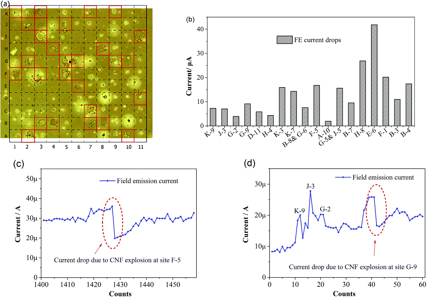 | ||
| Fig. 6 (a) The optical microscope image of the FEM patterns and 28 explosion patterns of the 11 × 11 freestanding CNF array on the PMMA thin film during the FE failure test. The FEM patterns left by the CNF emitter explosion are highlighted. The other FEM patterns are left by the FE electron exposure. (b) FE current drops right after explosions of CNF emitters of 20 sites. (c) An overall FE current drop of 16.76 μA is recorded right after the CNF emitter explosion at the site F-5. (d) An overall FE current drop of 9.14 μA is recorded right after the CNF emitter explosion at the site G-9. The impact of explosions of three other sites on the overall FE emission current is also shown. | ||
The current drop varies from emitter to emitter, ranging from a minimum 1.95 μA to a maximum 41.82 μA. The average current drop of the 20 disintegrated CNF emitters is 11.82 μA. Majority of current drops is around the average. Since CNF emitters at site B-8 and G-6 explode at almost the same moment, only one current drop of 7.59 μA is found. The same situation is found for the emitters at site G-5 and J-5, which have a current drop of 15.60 μA. We believe these current drops are the critical currents that cause the light emission and explosion of the corresponding CNF emitters. Due to the individual difference of CNF emitters in the array, the critical current that CNF emitters can withstand varies. An average emission current of 11.82 μA that causes CNF emitter failure agrees well with the maximum emission current of 10–20 μA from individual CNF that was investigated previously.35 Fig. 6(c) and (d) show the overall FE current drop right after the explosion of CNT emitter at the site F-5 and the site G-9, respectively. The overall FE current slightly increased before the explosion at the site F-5 occurs and then decreases by 16.76 μA right after the explosion. The explosion at the site G-9 occurs at an early stage of the FE test. The overall FE current shows a tendency of increase due to warm-up of the FEA. The FE current increased drastically before the explosion occurs at the site G-9 and then decreases by 9.14 μA after the explosion. We believe that the abrupt current increase and drop cause the CNF emitter at the site G-9 failure. Since the FEA is working at a constant voltage continuously, after the explosions the overall FE current tends to increase as the Joule heat accumulates.
4. Discussions
4.1 Coulomb explosion of CNF emitters induced by FE
Based on the above study, we attribute the disintegration of CNF emitters and the blasting of PMMA to Coulomb explosion.36 It is defined classically by Rayleigh instability limit, above which an excessively charged cluster becomes unstable and explodes into smaller fragments.37,38 In this case, we model the CNF emitter as a cylinder with a height of 5 μm and a diameter of 100 nm. The quantity of charges that a CNF emitter can hold is given by the Rayleigh limit.37,38| QR2 = 6π2ε0γl2r | (1) |
In the eqn (1), ε0 = 8.85 × 10⁻¹² F m−1 is the vacuum permittivity; γ = 40.3 mN m−1 is the surface tension coefficient of CNF;39 r = 50 nm is the radius of the CNF; l = 5 μm is the height of the CNF. The charges to overcome the Rayleigh limit are calculated to be 5.14 × 10⁻¹⁵ C. The charge on a CNF emitters during FE can be calculated from the relationship between the current and the charge:
| I = nAve | (2) |
In the eqn (2), I is the current; n is number of charged particles per unit volume; A is the cross-sectional area of the CNF emitter; v is the drift velocity; e is the charge on each particle. The drift velocity is a function of electron mobility, μ, and electric field, E.
| v = μE | (3) |
Since CNF is composed of stacked curved graphene layers, CNF has the similar properties as graphite.15 We choose the electron mobility of multi-layer graphene, which is 3000 cm2 V−1 s−1.40 Using eqn (2), the total charges on the CNF is 3.13 × 10⁻¹⁵ C. The linear charge density of is 6.25 × 10⁻¹⁰ C m−1, corresponding to 4.04e nm−1, which is comparable with that overcomes the van der Waals force among SWNT bundles.41 The charge on the CNF emitter is just the same order of magnitude as that of the Rayleigh limit. However, considering the size of annular crater on the PMMA thin film and the size of sputtered PMMA on the substrate, Coulomb energy not only overcomes the surface energy of CNF but also provides kinetic energy for the CNF fragments. Heating and chemical reaction is able to aid the Coulomb explosion.42,43 In this case, only Joule heating helps break the carbon chains at a lower electric field at the CNF surface. Besides, we also find that Joule heating alone cannot disintegrate CNF emitters. At site A-1, site J-7, and site B-10, there is only light emission observed at each site during the test. However, no damage is found in the SEM images of each CNF emitter at the three sites. Therefore, it is the Coulomb force of excessive charging with the aid of Joule heating that disintegrates the CNF. Fig. 7 presents the SEM images of the CNF emitters at the three sites after the FE test together with the video recording of light emission at each site.
 | ||
| Fig. 7 SEM images of CNF emitters at (a) site A-1, (b) site J-7, and (c) site B-10 after the experiment. Only light emission is observed at each site during the FE test. However no damage of each CNF emitter is found after the FE test. The insert of each SEM image is the video recording of the light emission at each corresponding site. The SEM images are taken at a tilted angle of 45°. | ||
Similar structure damage has been reported that electrical charging cause the outer layer of repelling from the main nanotube of MWNT emitters.22,23 After the CNF disintegrated, the fragments accelerated by the bias voltage touch the PMMA thin film surface. In the meantime, since the CNF has a tubular cone structure (Fig. S4†), the charged fragments retain an annular pattern of the CNF shell while expanding and flying towards the anode. When the charged fragments reach the PMMA thin film surface, an almost immediate release of electrons, from charged CNF fragments through the PMMA thin film to the anode, occurs and results in sputtering PMMA all around and an annular crater with PMMA pieces on the PMMA thin film surface due to the almost immediate electrons migration from CNF fragments to the PMMA thin film. This step is similar to the Coulomb explosion phenomenon of a piece of alkali metal drops into water.33 Considering the size of annular crater on the PMMA thin film and the size of a CNF emitter, such an impact is astonishing. The entire process is like firing a shotgun combined with pellets exploding on the target.
4.2 Joule heating of CNF emitters induced by FE
Joule heating is often reported in FE studies as a potential degradation of CNF emitters operating at large current.20,23,44 Moderate Joule heating can cause a rise in the overall FE current on the account of temperature dependence of FE.45,46 However, too much Joule heating causing the rise of emission current would cause more heat generated. The phenomenon of FE-induced light emission is previously observed when CNF emitter temperature is above 1500 K or a FE current of 20 μA, which increases in intensity as temperature rises.46,47 Considering the melted substrate and the light intensity variation observed at the corresponding CNF emitter failure sites, the light emission is an incandescence effect due to Joule heating, indicating that CNF emitters are working at a very high temperature. Therefore, the effect of temperature due to Joule heating during FE should be taken into account. Thermal equilibrium of Joule heating on CNF emitter can be obtained by heat dissipation. The maximum temperature of the CNF emitter due to Joule heating is determined by several parameters such as emission current, resistance, and size. Finite element analysis method is used to simulate this process. The transient study of CNF Joule heating during FE is performed by COMSOL Multiphysics software. The PECVD synthesized CNF has a thermal conductivity of around 80 W m−1 K−1.48 The specific heat is reported to be 713 J kg−1 K−1 and the mass density is around 1300 kg m−3. The resistance of PECVD CNF is reported to be 10−6 to 10−5 Ω m.35,49 The model here studied is a hollow cone structure with a base diameter of 100 nm, tip diameter of 35 nm, cone wall thickness of 20 nm, and a length of 5 μm. Heat loss in the simulation is caused by thermal radiation. Since the fabrication randomness that would cause the deviation of emitter size, two different CNF base diameters are compared. Fig. 8 presents finite element analysis of the effect of Joule heating on maximum temperature of CNF emitters during FE under different conditions.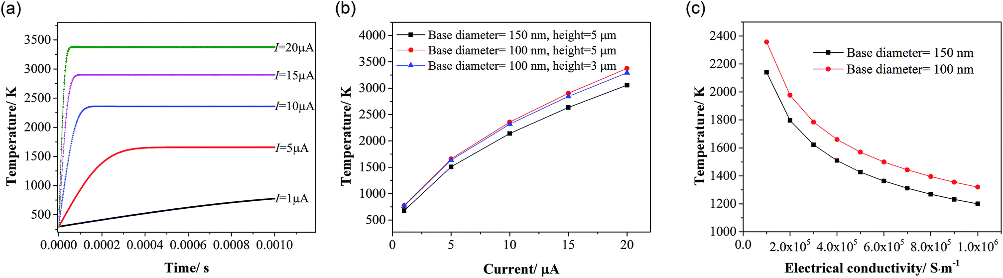 | ||
| Fig. 8 Finite element analysis results of the effect of Joule heating on maximum temperature of CNF emitters during FE. (a) CNF emitter temperature varies with time at different FE current. (b) Maximum temperature of CNF emitters of different base diameters and height varies with different FE current levels. (c) Temperature varies with electrical conductivity at 10 μA FE current. | ||
Fig. 8(a) shows that temperature of a CNF emitter at higher FE current reaches maximum temperature faster at the same conditions. However, it takes very short time (1 ms) for FE current to reach thermal equilibrium even at a FE current of 1 μA. Therefore, Joule heating of CNF emitters during FE at a certain critical current is almost an instantaneous process. Fig. 8(b) shows the maximum temperature of a CNF emitter can reach with different FE current levels. A thicker emitter is able to withstand higher critical FE current compared with a thinner one. While the CNF emitter height influences the critical FE current negatively compared with the effect of the CNF diameter. Fig. 8(c) illustrates the electrical conductivity of CNF emitters on the temperature of CNF at a constant current of 10 μA. A CNF emitter of higher electrical conductivity reaches lower temperature. The results also show that a FE current of 5 μA is able to heat a CNF emitter to over 1500 K. The average current drop of 11.82 μA can heat a CNF emitter to over 2500 K. Considering the melting point of Si and TiN which is 1687 K and 3203 K, respectively, a temperature over 2000 K is able to melt the silicon beneath the contact area, which would lose the support of CNF emitters. In practical situations, defects in CNF reduce the melting temperature of atoms around the defects.50
Theoretical analyses of electron emission over a wide range of temperatures and fields have been studied previously.51–53 Such thermal enhanced FE is defined as Schottky emission. Since this type of electron emission is a combined effect of electric field and heat, mathematical description of Schottky emission contains both effect of the electric field (E in volts per centimeter) and the temperature (T in Kelvin).51 For E ≤ 160T,1,33 the electron emission is classified as “Schottky emission”. For E ≤ 1100T,1,33 the electron emission is classified as “extended Schottky emission”. In our case, the bias voltage applied on the CNF FEA is 450 V. The distance between the anode and the cathode is 25 μm. Considering the our CNF emitter has an aspect ratio of 100, an enhanced electric field of 1.8 × 10⁷ V cm−1 is applied at the CNF emitter tip. Therefore, under such an electric field, extended Schottky emission is achieved at a temperature of 1447 K. Higher temperature causes the thermal induced electron emission becoming prominent and converts FE into Schottky emission regime. Therefore, the increasing electron emission current increases the CNF emitter temperature and generates more heat. Consequently, the high temperature weakens the CNF carbon bonds. As a result, the excessive charging on CNF emitters ultimately disintegrates the CNF emitters.
4.3 Mechanism of light emission and Coulomb explosion of CNFs induced by FE
Based on above study, the entire process of CNF emitter explosion can be represented in detail. At high FE current, Joule heating heats the CNF emitter to a high temperature. The high temperature increase the thermal induced electron emission and cause more electron emitted. In the meantime, light emission occurs and substrate begins to melt. With the aid of high temperature, excessive charging overcomes the van der Waals forces among graphite basal planes and CNF carbon bonds. Since the CNF has a tubular cone structure (Fig. S4†), the shell is broken apart by the charging on the CNF into charged fragments at high temperature. The charged fragments retain an annular pattern of the CNF shell while expanding and flying towards the anode. When the charged fragments reach the PMMA thin film surface, an almost immediate release of electrons, from charged CNF fragments through the PMMA thin film to the anode, occurs and results in another Coulomb explosion. The explosion blast away and sputter the PMMA debris and leaves an annular crater with PMMA pieces on the PMMA thin film surface.Due to the individual difference of CNF emitters in the array, the critical current that disintegrates CNF emitters varies. Finite element study shows that a thicker emitter is able to withstand higher critical FE current compared with a thinner one. While the CNF emitter height influences the critical FE current negatively compared with the effect of the CNF diameter. A CNF emitter of higher electrical conductivity reaches lower temperature. In practical situations, defects in CNF reduce the melting temperature of atoms around the defects. Therefore, thinner and taller CNF emitters with lower electrical conductivity and more defects are more likely to explode during FE.
In order to illustrate the mechanism of the Coulomb explosion of CNF induced by FE and the difference between normal FE and Coulomb explosion, we take four neighbouring CNF FE sites in the lower right corner of the 11 × 11 CNF FEA as an example. The four neighbouring sites are A-10, A-11, B-10, and B-11. The explosion sites on the substrate of these four sites is already shown in Fig. 4(f). Fig. 9 shows the illustration of the CNF Coulomb explosion process and a normal FE process from CNF emitters. These four sites contain all the FE status during the CNF emitter failure test. From the video recording and the FEM patterns (Fig. 9(c)) on the PMMA thin film surface, Coulomb explosion occurs at site A-10, a strong FE with light emission occurs at site B-10, and weak FE occurs at site A-11 and B-11. Explosion craters at site A-10 are clearly shown on the PMMA thin film. FE performance of the other three sites are distinguishable from the FEM patterns on the PMMA thin film.
 | ||
| Fig. 9 Illustration of the CNF Coulomb explosion process and a normal FE process from a CNF emitter: (a) a normal FE process; (b) a Coulomb explosion process of a CNF; (c) FEM patterns at site A-10, site A-11, site B-10, and site B-11 with a video recording of the corresponding sites inserted. The inserted video screenshot shows an explosion at site A-10 and a light emission at site B-10, which is also clearly reflected on the PMMA thin film. FEM patterns also indicate lighter FE performance from the site A-11 and B-11. | ||
5. Conclusions
This study represents the process of a light emission and Coulomb explosion induced by FE and demonstrates the CNF field emitter failure mechanism. The Coulomb explosion of CNF induced by FE is systematically characterized by the direct observation of the phenomenon using a microscopic camera, optical imaging and AFM study of the permanently damaged patterns of the PMMA thin film, and SEM imaging and EDS analysis of the explosion sites. The light emission, an incandescence effect due to Joule heating, is further investigated by finite element analysis and theoretical calculation. The light emission followed by the Coulomb explosion that causes CNF emitter failure is due to a combined effect of Joule heating and massive charging at high FE current. The FE current levels that disintegrate the CNF emitters range from 1.96 μA to 41.82 μA with an average of 11.82 μA. Joule heating is able to heat a CNF emitter to over 2500 K within a very short period, melt the contact area, and weaken the carbon bond and van der Waals force of graphite basal planes in the CNF. With the aid of Joule heating, extended Schottky emission is achieved at a temperature of 1447 K and excessive charging disintegrates the CNF emitters into charge fragments. Then an instantaneous release of electrons from CNF fragments through the PMMA thin film leading to the annular crater and the sputter of PMMA all around in a range of about 100 μm. The explosion generates an annular crater on the PMMA thin film of about 60–70 μm indicating a strong Coulomb energy that causes the Rayleigh instability. Besides, finite element study shows that during FE thinner and taller CNF emitters with lower electrical conductivity and more defects is likely to explode than others. This study successfully explains the mechanisms behind the absence of CNF emitters after FE, which is often simply attributed to uprooting or burning out of the emitter. The detailed study of Coulomb explosion of CNF induced by FE allows an insight of destruction of other nanowires during electrical transport and a systematic design of FE devices for long-lasting operation in practical applications. In addition, although Coulomb explosion destroys CNF emitters, considering such astonishing destruction, potential application of blasting and bombardment using CNF FE at micro-/nano-scale can be expected.Conflicts of interest
There are no conflicts to declare.Acknowledgements
This research was supported by Natural Sciences and Engineering Research Council of Canada, Canada Research Chair Grant, and University Health Network.References
- J. Jung, Y. Jin, J. Choi, Y. Park, T. Ko, D. Chung, J. Kim, J. Jang, S. Cha and W. Yi, Phys. B, 2002, 323, 71–77 CrossRef CAS.
- W. Milne, K. Teo, E. Minoux, O. Groening, L. Gangloff, L. Hudanski, J. Schnell, D. Dieumegard, F. Peauger and I. Bu, J. Vac. Sci. Technol., B: Microelectron. Nanometer Struct., 2006, 24, 345–348 CrossRef CAS.
- K. Teo, M. Chhowalla, G. Amaratunga, W. Milne, P. Legagneux, G. Pirio, L. Gangloff, D. Pribat, V. Semet and V. T. Binh, J. Vac. Sci. Technol., B: Microelectron. Nanometer Struct., 2003, 21, 693–697 CrossRef CAS.
- Y. Sun, D. A. Jaffray and J. T. W. Yeow, IEEE Trans. Electron Devices, 2013, 60, 464–470 CrossRef CAS.
- Y. Li, Y. Sun and J. Yeow, Nanotechnology, 2015, 26, 242001 CrossRef PubMed.
- R. J. Parmee, C. M. Collins, W. I. Milne and M. T. Cole, Nano Convergence, 2015, 2, 1 CrossRef.
- M. Chhowalla, C. Ducati, N. Rupesinghe, K. Teo and G. Amaratunga, Appl. Phys. Lett., 2001, 79, 2079–2081 CrossRef CAS.
- Y. Sun, J. T. W. Yeow and D. A. Jaffray, Small, 2013, 9, 3385–3389 CrossRef CAS PubMed.
- K. Teo, M. Chhowalla, G. Amaratunga, W. Milne, G. Pirio, P. Legagneux, F. Wyczisk, D. Pribat and D. Hasko, Appl. Phys. Lett., 2002, 80, 2011–2013 CrossRef CAS.
- L. Nilsson, O. Groening, C. Emmenegger, O. Kuettel, E. Schaller, L. Schlapbach, H. Kind, J. Bonard and K. Kern, Appl. Phys. Lett., 2000, 76, 2071–2073 CrossRef CAS.
- Z. F. Ren, Z. P. Huang, J. W. Xu, J. H. Wang, P. Bush, M. P. Siegal and P. N. Provencio, Science, 1998, 282, 1105–1107 CrossRef CAS PubMed.
- Z. Ren, Z. Huang, D. Wang, J. Wen, J. Xu, J. Wang, L. Calvet, J. Chen, J. Klemic and M. Reed, Appl. Phys. Lett., 1999, 75, 1086–1088 CrossRef CAS.
- K. Teo, S. Lee, M. Chhowalla, V. Semet, V. T. Binh, O. Groening, M. Castignolles, A. Loiseau, G. Pirio and P. Legagneux, Nanotechnology, 2003, 14, 204 CrossRef CAS.
- M. Chhowalla, K. Teo, C. Ducati, N. Rupesinghe, G. Amaratunga, A. Ferrari, D. Roy, J. Robertson and W. Milne, J. Appl. Phys., 2001, 90, 5308–5317 CrossRef CAS.
- A. V. Melechko, V. I. Merkulov, T. E. McKnight, M. Guillorn, K. L. Klein, D. H. Lowndes and M. L. Simpson, J. Appl. Phys., 2005, 97, 041301 CrossRef.
- M. Meyyappan, J. Phys. D: Appl. Phys., 2009, 42, 213001 CrossRef.
- G. Zhang, J. Chen, S. Z. Deng, J. C. She and N. S. Xu, Ultramicroscopy, 2009, 109, 385–389 CrossRef CAS PubMed.
- C. Li, Y. Zhang, M. T. Cole, S. G. Shivareddy, J. S. Barnard, W. Lei, B. Wang, D. Pribat, G. A. Amaratunga and W. I. Milne, ACS Nano, 2012, 6, 3236–3242 CrossRef CAS PubMed.
- M. Wang, L. Peng, J. Wang and Q. Chen, J. Phys. Chem. B, 2005, 109, 110–113 CrossRef CAS PubMed.
- J. Bonard, C. Klinke, K. A. Dean and B. F. Coll, Phys. Rev. B: Condens. Matter Mater. Phys., 2003, 67, 115406 CrossRef.
- J. Cumings, P. G. Collins and A. Zettl, Nature, 2000, 406, 586 CrossRef CAS PubMed.
- Z. L. Wang, R. P. Gao, W. A. de Heer and P. Poncharal, Appl. Phys. Lett., 2002, 80, 856–858 CrossRef CAS.
- M. Doytcheva, M. Kaiser and N. De Jonge, Nanotechnology, 2006, 17, 3226 CrossRef CAS.
- K. A. Dean and B. R. Chalamala, Appl. Phys. Lett., 2000, 76, 375–377 CrossRef CAS.
- J. Bonard, M. Croci, C. Klinke, R. Kurt, O. Noury and N. Weiss, Carbon, 2002, 40, 1715–1728 CrossRef CAS.
- Y. Li, Y. Sun, D. A. Jaffray and J. T. Yeow, Nanotechnology, 2017, 28, 155704 CrossRef PubMed.
- T. Döppner, T. Fennel, T. Diederich, J. Tiggesbäumker and K. Meiwes-Broer, Phys. Rev. Lett., 2005, 94, 013401 CrossRef PubMed.
- S. Shimizu, V. Zhakhovskii, F. Sato, S. Okihara, S. Sakabe, K. Nishihara, Y. Izawa, T. Yatsuhashi and N. Nakashima, J. Chem. Phys., 2002, 117, 3180–3189 CrossRef CAS.
- B. Manschwetus, T. Nubbemeyer, K. Gorling, G. Steinmeyer, U. Eichmann, H. Rottke and W. Sandner, Phys. Rev. Lett., 2009, 102, 113002 CrossRef CAS PubMed.
- X. Wei, D. Tang, Q. Chen, Y. Bando and D. Golberg, ACS Nano, 2013, 7, 3491–3497 CrossRef CAS PubMed.
- M. Lenner, A. Kaplan and R. Palmer, Appl. Phys. Lett., 2007, 90, 153119 CrossRef.
- H. Thomas, C. Bostedt, M. Hoener, E. Eremina, H. Wabnitz, T. Laarmann, E. Plönjes, R. Treusch, A. De Castro and T. Möller, J. Phys. B: At., Mol. Opt. Phys., 2009, 42, 134018 CrossRef.
- P. E. Mason, F. Uhlig, V. Vaněk, T. Buttersack, S. Bauerecker and P. Jungwirth, Nat. Chem., 2015, 7, 250–254 CrossRef CAS PubMed.
- R. Neutze, R. Wouts, D. van der Spoel, E. Weckert and J. Hajdu, Nature, 2000, 406, 752–757 CrossRef CAS PubMed.
- W. Milne, K. Teo, M. Chhowalla, G. Amaratunga, S. Lee, D. Hasko, H. Ahmed, O. Groening, P. Legagneux and L. Gangloff, Diamond Relat. Mater., 2003, 12, 422–428 CrossRef CAS.
- S. G. Kim, Y. H. Lee, P. Nordlander and D. Tománek, Chem. Phys. Lett., 1997, 264, 345–350 CrossRef CAS.
- L. Rayleigh, London, Edinburgh Dublin Philos. Mag. J. Sci., 1882, 14, 184–186 Search PubMed.
- O. Echt, P. Scheier and T. D. Märk, C. R. Phys., 2002, 3, 353–364 CrossRef CAS.
- S. Nuriel, L. Liu, A. Barber and H. Wagner, Chem. Phys. Lett., 2005, 404, 263–266 CrossRef CAS.
- K. Nagashio, T. Nishimura, K. Kita and A. Toriumi, Appl. Phys. Express, 2009, 2, 025003 CrossRef.
- G. Liu, Y. Zhao, K. Zheng, Z. Liu, W. Ma, Y. Ren, S. Xie and L. Sun, Nano Lett., 2008, 9, 239–244 CrossRef PubMed.
- J. Widmann, C. Aardahl and E. Davis, Aerosol Sci. Technol., 1997, 27, 636–648 CrossRef CAS.
- I. Last, Y. Levy and J. Jortner, Proc. Natl. Acad. Sci. U. S. A., 2002, 99, 9107–9112 CrossRef CAS PubMed.
- T. Ragab and C. Basaran, J. Appl. Phys., 2009, 106, 063705 CrossRef.
- Y. Sun, D. A. Jaffray and J. T. Yeow, Carbon, 2013, 58, 87–91 CrossRef CAS.
- S. Purcell, P. Vincent, C. Journet and V. T. Binh, Phys. Rev. Lett., 2002, 88, 105502 CrossRef CAS PubMed.
- J. M. Bonard, J. P. Salvetat, T. Stockli, L. Forro and A. Chatelain, Appl. Phys. A: Mater. Sci. Process., 1999, 69, 245–254 CrossRef CAS.
- X. J. Hu, A. A. Padilla, J. Xu, T. S. Fisher and K. E. Goodson, J. Heat Transfer, 2006, 128, 1109–1113 CrossRef CAS.
- L. Zhang, D. Austin, V. I. Merkulov, A. V. Meleshko, K. L. Klein, M. A. Guillorn, D. H. Lowndes and M. L. Simpson, Appl. Phys. Lett., 2004, 84, 3972–3974 CrossRef CAS.
- K. Zhang, G. M. Stocks and J. Zhong, Nanotechnology, 2007, 18, 285703 CrossRef.
- C. H. Hinrichs, W. A. Mackie, P. A. Pincosy and P. Poulsen, IEEE Trans. Electron Devices, 1990, 37, 2575–2580 CrossRef.
- L. Marton and C. Marton, Advances in electronics and electron physics, Academic Press, 1980 Search PubMed.
- M. Kiziroglou, X. Li, A. Zhukov, P. De Groot and C. De Groot, Solid-State Electron., 2008, 52, 1032–1038 CrossRef CAS.
Footnote |
| † Electronic supplementary information (ESI) available. See DOI: 10.1039/c7ra07474c |
| This journal is © The Royal Society of Chemistry 2017 |