
 Open Access Article
 This Open Access Article is licensed under a Creative Commons Attribution-Non Commercial 3.0 Unported Licence
Characteristics of an oxide/metal/oxide transparent conducting electrode fabricated with an intermediate Cu–Mo metal composite layer for application in efficient CIGS solar cell
San Kang†
,
R. Nandi†,
Jae-Kwan Sim,
Jun-Yong Jo,
Uddipta Chatterjee and
Cheul-Ro Lee *
*
Semiconductor Materials Process Laboratory, School of Advanced Materials Engineering, Engineering College, Research Center for Advanced Materials Development (RCAMD), Chonbuk National University, Baekje-daero 567, Jeonju 54896, Republic of Korea. E-mail: crlee7@jbnu.ac.kr
First published on 13th October 2017
Abstract
In order to improve the performance of Al-doped ZnO (AZO) based transparent conducting oxide (TCO) films, a metal Cu–Mo composite layer has been introduced between two AZO films to form an oxide/metal/oxide structure. The AZO/Cu–Mo/AZO (ACMA) multilayer film was prepared at room temperature by direct current magnetron sputtering equipped with multi-targets. To evaluate the performance of ACMA film as transparent conductors, the optical and electrical properties have been studied. These studies have shown the introduction of Cu–Mo composite layer significantly improves the performance of transparent conducting ACMA film compared to the AZO film as well as AZO/Cu/AZO (ACA) and AZO/Mo/AZO (AMA) multilayer films. The opto-electrical properties of the ACMA film critically depend on the thickness of the Cu–Mo composite layer. The highest figure of merit ∼7.96 × 10⁻⁴ Ω−1 is obtained for the ACMA film with a 10 nm thick Cu–Mo composite layer, indicating optimum conditions for the fabrication of transparent conducting electrodes. The CIGS solar cell fabricated with the ACMA electrode exhibits substantially higher efficiency (11.59%), compared to ACA or AMA electrodes. The gain in the cell efficiency is attributed to the improved opto-electrical characteristics of the ACMA electrode, resulting from the optimum optical transmittance and charge carrier collections.
1. Introduction
Transparent conducting oxide (TCO) materials are widely used in a variety of optoelectronic devices, such as flat-panel displays, thin-film transistors, electrochromic devices, gas sensors, liquid crystal displays, light emitting devices and solar cells owing to high optical transmittance in the visible region (>80%) and low electrical resistivity (<10−3 Ω cm).1–3 Indium tin oxide is the most commonly used TCOs for many years, which offers commercially acceptable performance in terms of high conductivity and optical transparency.4–6 However, the In element is toxic, less stable in hydrogen plasma and expensive due to the rapid depletion of the elemental indium sources.7,8 Thus it is essential to develop alternative indium-free or indium-reduced TCO thin films for optoelectronic applications. Various alternative TCOs, such as SnO2:F (FTO), SnO2:Sb (ATO) and ZnO:Al (AZO) have attracted considerable attention for the fundamental studies and optoelectronics, especially in photovoltaics.9–12Al-doped zinc oxide (AZO) thin film offers the advantages of low cost, nontoxicity, high transparency in visible region and reaction stability in hydrogen plasma.10,13 AZO is a n-type TCO has wide direct bandgap of 3.37 eV and large exciton binding energy of 60 meV. However, the conductivity of the AZO thin film is not high enough for practical application, and therefore limits the application in transparent conductors. Metal thin films display very low optical transparency in the visible region, but exhibit good conductivity. Therefore, various metal thin films, such as Ag, Au, Al, Mo and Cu metals in the form of thin films or nanostructures have been inserted between AZO films in order to improve the conductivity and maintain high optical transparency.14–19 Copper is a low cost high conductive material and is being widely used in VLSI technology. Yang et al.20 reported that the AZO/Cu/AZO film exhibited a figure of merit of 1.94 × 10⁻² Ω−1 and an average transmittance of 84% for a Cu thickness of 8 nm. Molybdenum is an ideal back electrode material which has been used in photovoltaic devices due to its high chemical stability, conductivity and melting point. Lin et al.21 has shown AZO/Mo/AZO film achieves a highest figure of merit of 2.23 × 10⁻⁴ Ω−1 by optimizing AZO and Mo layer thickness. In addition, bilayer metal films (Cu layer/Mo layer) or Cr–Cu metal composite layer also have been used to enhance the performance of AZO based TCOs.17,19
Copper indium gallium selenide (CIGS) based thin film solar cells are receiving worldwide attention for solar energy conversions in view of sustainable and renewable energy production.22,23 AZO based TCOs, act as a front contact (known as window layer), are already being used in the fabrication of CIGS solar cell at the industrial level.13,24 The conductivity, transparency and stability play an important role in the performance of solar cells. Recent studies have shown the efficiency of photovoltaic devices have been significantly improved by using oxide/metal/oxide based transparent conducting electrodes, in contrast to a simple oxide based electrodes.7,25,26 Therefore, AZO/metal/AZO based transparent conducting films with improved optical, electrical or structural properties promise an essential prerequisite for high efficient CIGS solar cells.
In the present work, we have investigated the performance of AZO based TCOs using an intermediate Cu–Mo composite layer. The AZO/Cu–Mo/AZO (ACMA) multilayer films with different Cu–Mo layer thickness were deposited by direct current (dc) magnetron sputtering. The structural, electrical and optical properties of the ACMA multilayer films have been studied. In order to examine the performance of ACMA films as a transparent conductor, CIGS solar cell has been fabricated with ACMA electrode. The opto-electrical properties and performance in CIGS solar cell fabricated with ACMA electrode also have been compared with the device fabricated with AZO/Cu/AZO (ACA) and AZO/Mo/AZO (AMA) electrodes.
2. Experimental
The ACMA films were deposited on PET (polyethylene terephthalate) substrate at room temperature by dc magnetron sputtering system equipped with multi-targets. Prior to the deposition, PET substrates were ultrasonically rinsed in de-ionized water, acetone and ethanol for 10 minutes each. The substrates were then dried in N2 flow and used for deposition. The target to substrate distance was ∼10 cm, and the base pressure was ∼2 × 10⁻⁶ Torr. In order to obtain a uniform deposition, the substrate holder was rotated at a frequency of 15 rpm. The deposition was carried out in argon (99.99%) atmosphere at a constant sputtering pressure of 3 × 10⁻³ Torr. The transparent conducting oxide films studied in the present work (ACMA, ACA and AMA) are consisted of three consecutive depositions. First, AZO films were deposited on PET substrate by magnetron sputtering of ceramic ZnO![[thin space (1/6-em)]](https://www.rsc.org/images/entities/char_2009.gif) :Al2O3 target (weight ratio ∼ (49:1)) in argon atmosphere at 150 W dc power for 6 minutes. Subsequently, the Cu–Mo composite layers were deposited on AZO films by co-sputtering of Cu and Mo targets (99.99%) in argon ambient at a dc power of 50 W at room temperature. The deposition time was varied from 10 to 60 seconds to optimize the thickness of Cu–Mo films. Finally, AZO films were deposited on Cu–Mo/AZO films by dc sputtering, as described above. The entire deposition process of ACMA film on PET substrate is schematically represented in Fig. 1. The details of the fabrication and characterization processes of CIGS solar cell have been reported earlier.27 Molybdenum (Mo) back contact electrode for CIGS solar cell was deposited on soda lime glass substrate by dc sputtering. The CIGS absorber layer was deposited on Mo film following the steps as described in ref. 27. About 65 nm thick n-type CdS buffer layer was then deposited on top of the CIGS absorption layer using chemical bath deposition. Then the transparent conducting electrodes (ACMA, ACA or AMA films) were deposited on CdS buffer layer by magnetron sputtering, as described above. Finally, Ag metal contacts were deposited by magnetron-sputtering to complete the fabrication of CIGS solar cells.
:Al2O3 target (weight ratio ∼ (49:1)) in argon atmosphere at 150 W dc power for 6 minutes. Subsequently, the Cu–Mo composite layers were deposited on AZO films by co-sputtering of Cu and Mo targets (99.99%) in argon ambient at a dc power of 50 W at room temperature. The deposition time was varied from 10 to 60 seconds to optimize the thickness of Cu–Mo films. Finally, AZO films were deposited on Cu–Mo/AZO films by dc sputtering, as described above. The entire deposition process of ACMA film on PET substrate is schematically represented in Fig. 1. The details of the fabrication and characterization processes of CIGS solar cell have been reported earlier.27 Molybdenum (Mo) back contact electrode for CIGS solar cell was deposited on soda lime glass substrate by dc sputtering. The CIGS absorber layer was deposited on Mo film following the steps as described in ref. 27. About 65 nm thick n-type CdS buffer layer was then deposited on top of the CIGS absorption layer using chemical bath deposition. Then the transparent conducting electrodes (ACMA, ACA or AMA films) were deposited on CdS buffer layer by magnetron sputtering, as described above. Finally, Ag metal contacts were deposited by magnetron-sputtering to complete the fabrication of CIGS solar cells.
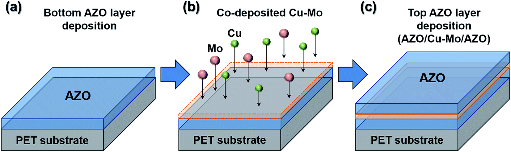 | ||
| Fig. 1 Schematic representation of the deposition processes of ACMA transparent conducting films. | ||
The surface morphology of the ACMA film was analyzed by using field-emission scanning electron microscopy (FE-SEM, Hitachi S-7400, Hitachi, Japan) with an operating voltage of 15 kV and atomic force microscopy (AFM, Parlo System XE-100). Crystal structure and orientation of the ACMA film were studied by X-ray diffraction (XRD) measurements using a Rigaku diffractometer equipped with a Cu-Kα radiation source. The optical transmittance spectra were recorded at room temperature by UV-VIS spectroscopy (UV/VIS-NIR spectrophotometer Shimadzu UV-3600). Electrical property of the films was determined by Hall measurements (Ecopia HMS 3000). CIGS solar cells were characterized by current–voltage measurements in dark and under illumination of Xenon lamp.
3. Results and discussion
The crystal structure and orientation of the sputter deposited ACMA multilayer films with different thickness of intermediate Cu–Mo composite layer were investigated by X-ray diffraction (XRD). The XRD patterns of the ACMA multilayer films are shown in Fig. 2(a). All the ACMA multilayer films exhibit a strong (002) reflections from hexagonal wurtzite AZO, indicating c-axis orientation of the films. The variation of full width at half maximum (FWHM) and the grain size of ACMA films with the thickness of Cu–Mo composite layer is shown in Fig. 2(a). FWHM values of the (002) diffraction peak gradually decreases with increase in the thickness of Cu–Mo composite layer of ACMA films. The grain size of the AZO films were calculated from the (002) reflections using Scherrer's formula.28 It is observed that the grain size of the AZO increases from 12 nm to 25 nm with increase in the thickness of Cu–Mo composite layer from 6 nm to 31 nm. These results imply that the introduction of metal composite layer improves the crystalline quality of top AZO film. | ||
| Fig. 2 (a) XRD patterns of ACMA multilayer films with different thickness of Cu–Mo composite layer; (b) grain size and FWHM of (002) reflection of ACMA multilayer films with different thickness of Cu–Mo composite layer; (c) optical transmittance spectra of ACMA multilayer films with different thickness of Cu–Mo composite layer; (d) dependence of sheet resistance and figure of merits of ACMA multilayer films on the thickness of Cu–Mo composite layer. | ||
Fig. 2(c) displays the optical transmittance spectra in the wavelength range of 300–1000 nm of the ACMA multilayer films with different thickness of Cu–Mo composite layer. The average optical transmittance (%) at wavelength of ∼500 nm for all the ACMA films is summarized in Table 1. The average optical transmittance of the AZO film without the Cu–Mo composite layer is ∼85%. Introduction of a ∼6 nm thick intermediate Cu–Mo composite layer results in a decrease in the optical transmittance to ∼82%. Further increase in the thickness of the Cu–Mo composite layer leads to a monotonous decrease in the optical transmittance and the average optical transmittance is ∼62% for ∼31 nm thick Cu–Mo composite layer. Decrease in optical transmittance with the thickness of Cu–Mo composite layer is primarily attributed to the increase in the absorption as well as reflection losses from the ACMA film. However, the enhancement in light scattering due to the larger grain size of AZO films may also contribute to the lower optical transmittance of ACMA films with thicker Cu–Mo layer.
| AZO/Cu–Mo/AZO deposition time (min2 s−1) | 6/0/6 | 6/10/6 | 6/15/6 | 6/20/6 | 6/30/6 | 6/45/6 | 6/60/6 |
|---|---|---|---|---|---|---|---|
| Cu–Mo thickness (nm) | 0 | 6 | 10 | 12 | 17 | 23 | 31 |
| Average transmittance (%) | 85.07 | 81.70 | 77.95 | 76.96 | 73.28 | 67.48 | 62.66 |
| Sheet resistance (Ω sq−1) | 20000 |
232 | 104 | 91 | 64 | 53 | 42 |
| Figure of merit (×10−4 Ω−1) | 0.09 | 5.71 | 7.96 | 7.67 | 6.97 | 3.69 | 2.22 |
The sheet resistances of the ACMA films as a function of the thickness of Cu–Mo composite layer are presented in Table 1. From the tabular data it is observed that the presence of Cu–Mo composite layer significantly influences the sheet resistance of the ACMA films. The sheet resistance is found to decrease with in the thickness of Cu–Mo composite layers. Following the parallel circuit model, the total sheet resistance (Rs) of the ACMA multilayer film is approximately equal to the parallel resistance of the AZO (RAZO) and metal (RCu–Mo) films.27
 | (1) |
Introduction of ∼6 nm thick Cu–Mo layer in ACMA film results in a drastic decrease of sheet resistance from 20000 Ω sq−1 to 232 Ω sq−1. Further increase in the thickness of Cu–Mo layer leading to a monotonous decrease in the sheet resistance and attains a lowest value of 42 Ω sq−1 for ∼31 nm thick Cu–Mo layer. It is well known that the conductivity of metal film is several orders of magnitude higher than that of AZO film. Therefore, the conductivity of the ACMA multilayer films is mainly dominated by the conductivity of the Cu–Mo composite layer. As a result, the sheet resistance of the AZO films decreases with the introduction of metal Cu–Mo composite layer.
The performance of transparent conducting films is well known to be affected by the optical transmittance and sheet resistance. Ideally, both optical transmittance and electrical conduction of transparent conductors should be as high as possible. However, above results reveal that the optical transmittance decreases in contrast to the increase in the conductivity of ACMA multilayer films. In order to optimize the performance of transparent conducting ACMA films, the figure of merit (FOM) of the ACMA films is calculated from the optical transmittance and sheet resistance.29 The calculated FOM values of ACMA films with different thickness of Cu–Mo composite layers are listed in Table 1. The AZO film without the Cu–Mo composite layer exhibit lower FOM values, due to the high sheet resistance of the AZO film. Decrease in sheet resistance with introduction of ∼6 nm thick Cu–Mo composite layer in ACMA films results in an increase in the FOM value. However, in spite of inferior optical transmittance and sheet resistance, ACMA films achieves the highest FOM value of 7.96 × 10⁻⁴ Ω−1 for ∼10 nm thick Cu–Mo composite layer, indicating the best electrical and optical performance among all the ACMA films. A gradual decrease in FOM values is observed when the thickness of Cu–Mo composite layer increases from 12 nm to 31 nm, due to declined optical transmittance. These results indicate that the ACMA film with ∼10 nm Cu–Mo composite layer exhibits optimum optical transparency and electrical conductivity for the application in transparent electrodes.
The surface morphology of the sputtered ACMA multilayer films was examined by the FE-SEM and AFM. Fig. 3(a) shows the cross-sectional FE-SEM image of a typical ACMA multilayer film deposited on PET substrate with a ∼10 nm thick Cu–Mo composite layer. It is observed that all the three layers are uniform and compact in nature. The AFM image of the AZO film deposited on ∼10 nm thick Cu–Mo composite layer is shown in Fig. 3(b). AFM image displays the AZO grains are uniformly distributed over the Cu–Mo layer and the average lateral grain size is 30 ± 5 nm. The root mean square surface roughness of the AZO film is found to be 10.0 ± 0.1 nm. These results are in accordance with the FE-SEM image (top surface) of AZO film, as shown in the inset of Fig. 3(b).
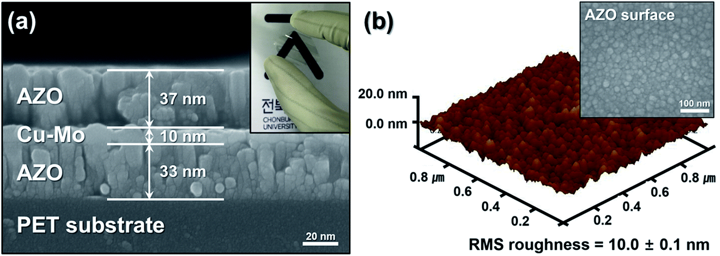 | ||
| Fig. 3 (a) Cross-sectional FE-SEM image of the sputtered ACMA multilayer film deposited on PET substrate (inset shows the optical image of ACMA film showing high optical transparency); (b) AFM image of AZO film deposited on 10 nm thick Cu–Mo composite layer/AZO. Inset shows the top surface of AZO film (FE-SEM image). | ||
The surface morphology and elemental compositions of the sputtered Cu–Mo composite film deposited on bottom AZO film were also analyzed by FE-SEM and energy-dispersive X-ray spectroscopy (EDS), and these results are presented in Fig. 4. FE-SEM image (Fig. 4(a)) reveals that the sputtered Cu–Mo composite film is uniform, compact and exhibits remarkably smooth surface. The EDS elemental mapping of Cu and Mo (Fig. 4(b) and (c)) showed that both the elements are uniformly distributed over the AZO film. The intensity signal counts and mass ratios between Cu and Mo of the Cu–Mo composite film are shown in Fig. 4(d). The Cu–Mo composite film is found to be considerably Cu rich. This is associated with the higher sputtering rate of copper due to its higher sputtering yield than that of molybdenum.
 | ||
| Fig. 4 (a) FE-SEM image of the sputtered Cu–Mo composite layer deposited on AZO film; (b) and (c) elemental mapping of Cu–Mo composite layer; (d) elemental analysis report of Cu–Mo composite layer. | ||
Furthermore, the electrical and optical properties of the ACMA films were also compared with the ACA and AMA films with identical thickness (∼10 nm) of metal layers. Fig. 5 depicts the optical transmittance spectra of ACA and AMA films, in which the transmittance spectrum of ACMA film is also included. A comparison of the optical transmittance, sheet resistance, resistivity and FOM values of the proposed AZO/metal/AZO films from the recent literatures are listed in Table 2. The corresponding values for the ACA, AMA and ACMA films obtained from the present work are also listed Table 2. The tabulated data shows that the ACMA film exhibits higher optical transmittance (∼78%), compared to the ACA and AMA films. On the other hand the sheet resistance of the ACMA film is inferior (104 Ω sq−1) to the ACA or AMA films. Nevertheless, the FOM value of ACMA film is substantially higher than that of ACA and AMA films. From a comparison with Tables 1 and 2, it is also seen that the ACMA film with ∼6 nm thick Cu–Mo composite layer displays superior opto-electrical performance than that of ACA or AMA films with thicker (∼10 nm) metal layers (Cu or Mo). Therefore, it can be concluded that the introduction of Cu–Mo composite layer between the AZO films significantly improves the performance of transparent conducting ACMA films compared to the AZO films as well as AZO film sandwiched with simple Cu or Mo metal layer. It is worthwhile to mention, the FOM value for the ACMA film is quite comparable to the recently reported for AZO/3 nm Cu/6 nm Mo/AZO films.19
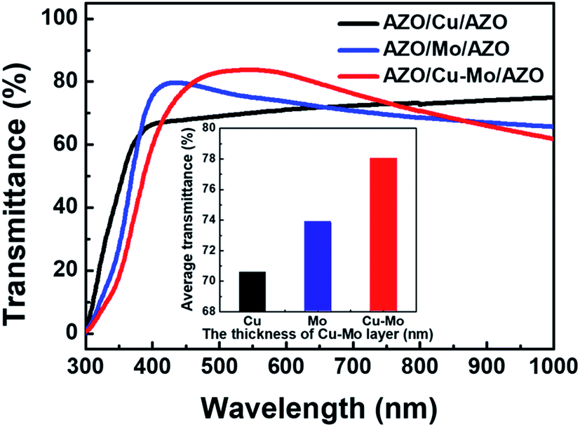 | ||
| Fig. 5 Optical transmittance spectra of ACA, AMA and ACMA transparent conducting films. | ||
| AZO/Metal/AZO | Thickness (nm) | Average transmittance (%) | Sheet resistance (Ω sq−1) | Resistivity (Ω cm) | Figure of merit (Ω−1) | Ref. |
|---|---|---|---|---|---|---|
| AZO/Ag/AZO | 37/10/37 | 87.4 | 6 | — | 5.29 × 10⁻² | 30 |
| AZO/Au/AZO | 45/8/45 | 80.8 | 8 | — | 1.46 × 10⁻² | 31 |
| AZO/Ni/AZO | 50/5/50 | 84.7 | 493 | 4.86 × 10⁻³ | 3.14 × 10⁻⁴ | 32 |
| AZO/Pd/AZO | 50/7/50 | 83.2 | 45 | 4.8 × 10⁻⁴ | 3.53 × 10⁻³ | 33 |
| AZO/Mo/AZO | 30/15/30 | 80 | 13 | 9 × 10⁻⁵ | 5.95 × 10⁻² | 34 |
| AZO/Cu/AZO | 40/8/40 | 84 | 9 | 7.92 × 10⁻⁵ | 1.94 × 10⁻² | 35 |
| AZO/Zr–Cu/AZO | 50/2/50 | 80 | 43 | — | 1.42 × 10⁻³ | 36 |
| AZO/Ag–Ti/AZO | 70/10/70 | 83 | — | 4.95 × 10⁻⁴ | 8.93 × 10⁻³ | 37 |
| AZO/Cu–Cr/AZO | 55/9/55 | 85 | 94 | — | 2.1 × 10⁻³ | 38 |
| AZO/Cu/Mo/AZO | 50/3/6/50 | 78 | 45 | — | 9.78 × 10⁻⁴ | 19 |
| AZO/Cu/AZO (ACA) | 37/10/33 | 70.6 | 65 | — | 4.73 × 10⁻⁴ | This work |
| AZO/Mo/AZO (AMA) | 37/10/33 | 73.8 | 276 | — | 1.74 × 10⁻⁴ | |
| AZO/Cu–Mo/AZO (ACMA) | 37/10/33 | 77.9 | 104 | — | 7.96 × 10⁻⁴ |
In order to investigate the performance of ACMA film as transparent conductor in CIGS solar cell, a CIGS solar cell has been fabricated utilizing ACMA film deposited under optimized condition. A typical device structure of the fabricated CIGS solar cell is schematically shown in Fig. 6(a). CIGS solar cells also have been fabricated with transparent conducting ACA and AMA electrodes for the comparison. Fig. 6(b) illustrates the J–V characteristic curves of the CIGS solar cells fabricated with ACA, AMA and ACMA electrodes. The device parameters of all the CIGS solar cells are tabulated in Table 3. The CIGS solar cell fabricated with ACMA electrode exhibits the highest efficiency of 11.59% with short circuit current density (Jsc) of 30.16 mA cm−2, open circuit voltage (Voc) of 535 mV and fill factor (FF) of 71%. However, the obtained Voc and FF values are nearly identical for all the devices, suggests no significant change in the recombination characteristics and series resistances of the solar cells resulting from electrode choice. From a comparison with Tables 1 and 2, it is also noticed that the cell efficiency is strongly depends on the electrical and optical properties of transparent conductors in terms of figure of merits. It is only the short circuit current density (Jsc) which primarily determines the performance of the solar cells. In other words, the cell efficiency is predominantly depends on the carrier generation in the absorber layers and collection at the electrodes. The solar cell fabricated with AMA electrode displays low efficiency (9.01%), arising from the poor performance of the AMA electrode due to the smaller FOM (1.74 × 10⁻⁴ Ω−1). ACA based device shows an improvement in cell efficiency over AMA based device increasing from 9.01% to 10.83%. The AMA films exhibit higher optical transmittance thus higher carrier generation in the absorber layers, but the cell efficiency is limited by the poor carrier collections due to high sheet resistance. The marginal improved device performance in the case of ACA films is attributed to the better collections at the electrodes because of the smaller sheet resistance. Interestingly, the ACMA film with highest FOM (7.96 × 10⁻⁴ Ω−1) value displays substantially enhanced cell efficiency of 11.59%. It is also important to mention that, the efficiency of CIGS solar cell fabricated with AMA, ACA and ACMA electrodes is significantly higher than the our recent demonstration of AZO (without any metal layer) electrode based device.27 It has also been reported that the efficiency of photovoltaic devices can be improved by using oxide/metal/oxide electrodes, in contrast to simple oxide electrodes.7,25,26 Therefore, it is believed that the gain in the efficiency of the solar cell is attributed to the improved opto-electrical characteristics, resulting from the optimum optical transmittance and charge carrier collections of the transparent conducting ACMA electrodes. These studies suggest that the device performance of CIGS solar cell can be significantly improved by using the Cu–Mo composite layer with optimum thickness in contrast to a simple Cu or Mo metal layers stacked between AZO films.
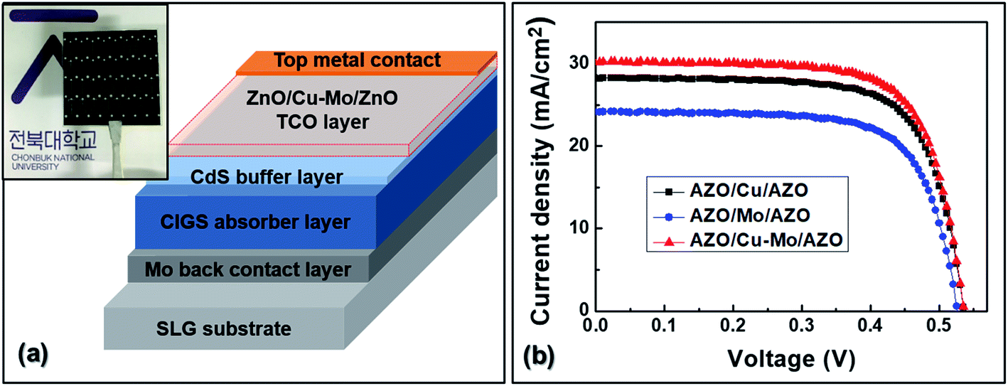 | ||
| Fig. 6 (a) Schematic diagram of the fabricated CIGS solar cell (inset shows optical image of the device); (b) current density vs. voltage graph of CIGS solar cell fabricated with different transparent conducting films. | ||
| Electrodes | Voc (mV) | Jsc (mA cm−2) | Fill factor (%) | Efficiency (%) |
|---|---|---|---|---|
| AZO/Cu/AZO | 535 | 28.21 | 71.73 | 10.83 |
| AZO/Mo/AZO | 525 | 24.09 | 71.14 | 9.01 |
| AZO/Cu–Mo/AZO | 535 | 30.16 | 71.73 | 11.59 |
4. Conclusion
In summary, the opto-electrical characteristics of AZO based TCOs have been improved by using an intermediate Cu–Mo composite layer stacked between AZO films. The transparent conducting ACMA films with different thickness of Cu–Mo composite layer were prepared by direct current magnetron sputtering. The ACMA films are consisted of uniformly distributed three distinct layers (top AZO, intermediate Cu–Mo composite and bottom AZO layer) displaying compact morphology. The AZO film without any metal layer exhibits higher optical transmittance, but the large sheet resistance limits the performance as transparent conductor. Introduction of metal layer (Cu or Mo) significantly improves the transparent conducting properties of AZO film. The performance of the AZO film was further improved by introducing intermediate Cu–Mo metal composite layers, instead of simple Cu or Mo layers. The ACMA (AZO/Cu–Mo/AZO) film showed superior transparent conducting properties compared to the AZO film as well as ACA or AMA films by means of figure of merit. The thickness of the Cu–Mo composite layer has a great influence in the opto-electrical properties of ACMA film. The highest figure of merit value of ∼7.96 × 10⁻⁴ Ω−1 is obtained for ACMA film with ∼10 nm thick Cu–Mo composite layer, indicating optimum conditions for the fabrication of transparent conducting electrodes. The ACMA film with thin Cu–Mo composite layer is also displayed superior opto-electrical performance than the ACA or AMA films with thicker metal layers (Cu or Mo). The superior transparent conducting properties of the ACMA film is attributed to the high optical transmittance and inferior sheet resistance compared to the ACA and AMA films. The cell efficiency of CIGS solar cell fabricated with ACMA electrode (11.59%) is substantially higher than the ACA or AMA electrodes. The gain in the cell efficiency of CIGS solar cell using ACMA electrode is attributed to the improved opto-electrical characteristics, resulting from the optimum optical transmittance and charge carrier collections of the electrodes. The performance of the ACMA transparent conducting electrodes can be further improved by optimizing thickness, composition and structural properties of Cu–Mo composite layer for future high efficient CIGS solar cell.Conflicts of interest
The authors declare no competing financial interest.Acknowledgements
This work was supported by the National Research Foundation of Korea (NRF) grant funded by the Korea government (MSIP) (No. 2015R1A2A2A01002877) and (No. 2015R1A4A1042417).References
- C. G. Granqvist, Sol. Energy Mater. Sol. Cells, 2007, 91, 1529–1598 CrossRef CAS.
- L. He and S. C. Tjong, Mater. Sci. Eng., R, 2016, 109, 1–101 CrossRef.
- A. Mirzaei and G. Neri, Sens. Actuators, B, 2016, 237, 749–775 CrossRef CAS.
- D. S. Hecht, L. Hu and G. Irvin, Adv. Mater., 2011, 23, 1482–1513 CrossRef CAS PubMed.
- G. Haacke, Annu. Rev. Mater. Sci., 1977, 7, 73–94 CrossRef CAS.
- A. Kumar and C. Zhou, ACS Nano, 2010, 4, 11–14 CrossRef CAS PubMed.
- W. Tsai, S. R. Thomas, C. Hsu, Y. Huang, J. Tseng, T. Wu, C. Chang, Z. M. Wang, J. Shieh, C. Shen and Y. Chueh, J. Mater. Chem. A, 2016, 4, 6980–6988 CAS.
- E. M. Bomhard, Environ. Toxicol. Pharmacol., 2016, 45, 282–294 CrossRef CAS PubMed.
- J. Tian and G. Cao, Coord. Chem. Rev., 2016, 320–321, 193–215 CrossRef CAS.
- R. M. Pasquarelli, S. Ginley and R. O. Hayre, Chem. Soc. Rev., 2011, 40, 5406–5441 RSC.
- S. C. Dixon, D. O. Scanlon, J. Carmalt and I. P. Parkin, J. Mater. Chem. C, 2016, 4, 6946–6961 RSC.
- E. Fortunato, D. Ginley, H. Hosono and D. C. Paine, MRS Bull., 2007, 32, 242–247 CrossRef CAS.
- J. Rousset, F. Donsanti, P. Genevée, G. Renou and D. Lincot, Sol. Energy Mater. Sol. Cells, 2011, 95, 1544–1549 CrossRef CAS.
- T. Dimopoulos, M. Bauch, R. A. Wibowo, N. Bansal, R. Hamid, M. Auer, M. Jäger and E. J. W. List-kratochvil, Mater. Sci. Eng., B, 2015, 200, 84–92 CrossRef CAS.
- J. Ho, D. Kim, S. Kim, Y. Yoo, J. Hwan, S. Kim and T. Seong, Ceram. Int., 2016, 42, 3473–3478 CrossRef.
- Y. L. Y. Huang, J. Mater. Sci.: Mater. Electron., 2013, 24, 3058–3062 CrossRef.
- T. Lin, W. Huang and F. Tsai, Thin Solid Films, 2015, 589, 446–450 CrossRef CAS.
- S. Yu, L. Li, X. Lyu and W. Zhang, Sci. Rep., 2016, 6, 20399 CrossRef CAS PubMed.
- Y. Guo, W. Cheng, J. Jiang, S. Zuo and F. Shi, Vacuum, 2016, 131, 164–169 CrossRef CAS.
- T. Yang, Z. Zhang, S. Song and Y. Li, Vacuum, 2009, 83, 257–260 CrossRef.
- T. Lin, W. Huang and F. Tsai, Int. J. Mater. Sci. Appl., 2014, 3, 205–209 Search PubMed.
- J. Ramanujam and U. P. Singh, Energy Environ. Sci., 2017, 10, 1306–1319 CAS.
- M. Theelen and F. Daume, Sol. Energ., 2016, 133, 586–627 CrossRef CAS.
- F. Tsin, A. Venerosy, J. Vidal, S. Collin, J. Clatot, L. Lombez, M. Paire, S. Borensztajn, C. Broussillou, P. P. Grand, S. Jaime, D. Lincot and J. Rousset, Sci. Rep., 2015, 5, 8961 CrossRef CAS PubMed.
- Z. Zhao and T. L. Alford, Sol. Energy Mater. Sol. Cells, 2016, 157, 599–603 CrossRef CAS.
- J. Qi, Y. Li, T. Duong, H. Choi and S. Yoon, J. Alloys Compd., 2013, 556, 121–126 CrossRef CAS.
- S. Lee, J. Sim, N. J. S. Kissinger, I. Song, J. Kim, B. Baek and C. Lee, J. Alloys Compd., 2015, 633, 31–36 CrossRef CAS.
- A. L. Patterson, Phys. Rev., 1939, 56, 978–982 CrossRef CAS.
- G. Haacke, J. Appl. Phys., 1976, 47, 4086 CrossRef CAS.
- A. Bingel, M. Steglich, P. Naujok, R. Müller, U. Schulz, N. Kaiser and A. Tünnermann, Thin Solid Films, 2016, 616, 594–600 CrossRef CAS.
- T. Van Dang, S. V. N. Pammi, J. Choi and S. G. Yoon, Sol. Energy Mater. Sol. Cells, 2017, 163, 58–65 CrossRef.
- M. M. D. Kumar, S. Mi Baek and J. Kim, Mater. Lett., 2014, 137, 132–135 CrossRef CAS.
- W. Zhang, J. Xiong, L. Liu, X. Zhang and H. Gu, Sol. Energy Mater. Sol. Cells, 2016, 153, 52–60 CrossRef CAS.
- H. W. Wu and C. H. Chu, Mater. Lett., 2013, 105, 65–67 CrossRef CAS.
- S. Song, T. Yang, M. Lv, Y. Li, Y. Xin, L. Jiang, Z. Wu and S. Han, Vacuum, 2010, 85, 39–44 CrossRef CAS.
- J. Cheng, G. Cao, H. Zong, C. Kang, E. Jia and B. Zhang, Results Phys., 2017, 7, 910–913 CrossRef.
- W. C. Shih, K. S. Kao, D. L. Cheng, C. J. Chung, P. T. Hsieh and S. L. Ou, Surf. Coat. Technol., 2013, 219, 139–143 CrossRef CAS.
- T. Lin, W. Huang and F. Tsai, Microelectron. Eng., 2017, 167, 85–89 CrossRef CAS.
Footnote |
| † Equal contributor. |
| This journal is © The Royal Society of Chemistry 2017 |