
 Open Access Article
 This Open Access Article is licensed under a
 Creative Commons Attribution 3.0 Unported Licence
Use of a passivation layer to improve thermal stability and quality of a phosphorene/AZO heterojunction diode
Sushil Kumar Pandeya,
Nezhueyotl Izquierdoa,
Rick Liptakb and
Stephen A. Campbell *a
*a
aDepartment of Electrical and Computer Engineering, University of Minnesota, 200 Union Street, Minneapolis, Minnesota 55455, USA. E-mail: campb001@umn.edu
bPhysics and Optical Engineering, Rose–Hulman Institute of Technology, 5500 Wabash Ave, Terre Haute, IN 47803, USA
First published on 28th September 2017
Abstract
Herein, we report the effect of passivation layer composition on thermal stability as measured by Raman spectra of a phosphorene/Al-doped ZnO (AZO) heterostructure. Few-layer phosphorene was formed using micromechanical exfoliation on an AZO film/Si substrate. Samples were passivated by Al2O3, Si3N4, or an Al2O3/Si3N4 stack. Both films were deposited by atomic layer deposition. When these samples were annealed at temperatures in the range from 100 to 550 °C, the nitride-only structure was found to have highest thermal sustainability, demonstrating phonon peaks of out-of-plane (Ag1) and in-plane (B2g and Ag2) modes up to the highest temperature tested (550 °C). This was 100 °C higher than that for the samples with the conventionally used Al2O3 coating. An oxide/nitride stack permitted anneals up to 500 °C. For anneals up to 200 °C, the nitride-only passivated phosphorene film was found to have a significant red shift in all the three peaks. This is attributed to the effects of tensile strain. At annealing temperatures higher than 200 °C, the spectra blue shifted, attaining values close to the bulk peak position; this suggested strain relaxation in the film at higher temperatures. This relaxation was also evident from a reduction in the full-width at half maximum of the Raman phonon peaks at higher annealing temperatures. Further study suggests that this shift may be due to a reduction in the stress of the passivation layer. The improvement in thermal stability is believed to be due to silicon nitride acting as a diffusion barrier, blocking phosphorus out-diffusion. To demonstrate the utility of higher temperature annealing, a phosphorene/AZO heterojunction diode was fabricated with a Si3N4 passivation layer. The passivated device shows a significant improvement of the diode ideality factor with an increased annealing temperature. The improvement of the diode ideality factor is due to the significant reduction of defect concentration at high annealing temperatures. These findings will promote the development of high-performance phosphorene-based heterojunction devices.
I. Introduction
Atomically thin two-dimensional (2D) materials, such as graphene and transition metal dichalcogenides (TMDs), have made a significant impact in the field of electronic and optoelectronic devices.1–6 Graphene, however, has no band gap; this creates hurdles for its many device applications.7 Similarly, the modest carrier mobility of TMD materials makes them less suitable for high performance electronic and optoelectronic device applications.2,8,9 Phosphorene has attracted significant interest owing to its unique anisotropic manner, layer-dependent direct band gaps, high carrier mobility, and quasi-one dimensional (1D) excitonic nature that are not present in the abovementioned 2D materials.10–18 Phosphorene has a band gap of ∼0.3 eV in the bulk form, which increases with the reducing layer thickness, approaching ∼2 eV for the monolayer.10–18 As a result, there have been numerous reports on FETs and inverters fabricated in the material system. Phosphorene is also becoming an interesting material in the fabrication of solar cells and photodetectors. Theoretical studies predict that phosphorene bilayer-based solar cells have the capacity to produce an external quantum efficiency (EQE) of up to 18% in a flexible format.14 Phosphorene heterojunction p–n diodes, although embryonic, have also been reported.18–20 These heterojunctions are generally made with other 2D materials (i.e. TMDs) and thus use van der Waals junctions. The van der Waals interface plays an important role in electronic and optoelectronic devices. Researchers are also trying to realize 2D/3D heterojunction-based devices because the processing technology for 3D materials is well established. ZnO is generally recognized as a promising 3D material for short-wavelength optoelectronics devices due to its direct wide band gap of 3.37 eV and a large exciton binding energy of 60 meV.21–23 Thus, the heterostructure of phosphorene/ZnO can be potentially used for devices such as wide-band photodetectors.Often, 2D heterostructures exhibit poor interfaces, especially when formed with a 3D material. The device fabrication process characteristically requires a thermal annealing process to improve this interface. However, improved thermal stability after 2D material deposition provides additional flexibility to deposit subsequent layers needed for a device. However, this annealing process is rarely investigated in the reported phosphorene/3D material-based devices. The selection of the annealing conditions is estimated to influence both the properties of phosphorene film and the ultimate device performance. Herein, we investigated the effect of annealing temperature on the Raman phonon peaks of a phosphorene/Al-doped ZnO (AZO) heterostructure having different types of passivation layers. We have also made heterostructure diodes and studied the effect of annealing temperature on the ideality factor to point out the utility of this passivation.
II. Methods
Bulk black phosphorus crystals were prepared using red phosphorus, Sn, and SnI4 in the mass ratio 42![[thin space (1/6-em)]](https://www.rsc.org/images/entities/char_2009.gif) :2:1 following the method developed by Nilges.24 The materials were loaded into a 25 cm long fused silica ampoule. The ampoule was then evacuated to 10−5 Pa and sealed using an oxyacetylene torch. In the next step, the ampoule was loaded into a furnace, and temperature was slowly ramped to the growth condition, where the temperatures of the source and growth ends of the ampoule were kept at 650 °C and 600 °C, respectively. This temperature condition was maintained for two hours and then ramped down, and the ampoule was allowed to cool down to room temperature. After the completion of cooling, the black phosphorus crystals were obtained by breaking the ampoule in a glove box. Few-layer black phosphorene flakes were deposited by mechanically exfoliating the bulk black phosphorus crystal onto AZO/Si at room temperature. A 20 nm AZO thin film was deposited on a Si substrate by atomic layer deposition (Savannah series from Cambridge Nano Tech Inc.). Prior to AZO deposition, the Si substrates were rinsed thoroughly with trichloroethylene, acetone, isopropanol, and deionized (DI) water and purged by 99.999% pure nitrogen gas to remove dust particles and other contaminants. Finally, these phosphorene/AZO/Si samples were passivated by Al2O3, Si3N4, and Al2O3/Si3N4 stack deposited by plasma-enhanced atomic layer deposition (PE-ALD) (Fiji 200 Gen 2 from UltraTech). The thicknesses of the Al2O3 and Si3N4 passivation layers were kept constant, 6.5 nm in all the samples. Annealing was carried out in RTP-600S for 60 seconds under a flow of Ar at 10 sccm.
:2:1 following the method developed by Nilges.24 The materials were loaded into a 25 cm long fused silica ampoule. The ampoule was then evacuated to 10−5 Pa and sealed using an oxyacetylene torch. In the next step, the ampoule was loaded into a furnace, and temperature was slowly ramped to the growth condition, where the temperatures of the source and growth ends of the ampoule were kept at 650 °C and 600 °C, respectively. This temperature condition was maintained for two hours and then ramped down, and the ampoule was allowed to cool down to room temperature. After the completion of cooling, the black phosphorus crystals were obtained by breaking the ampoule in a glove box. Few-layer black phosphorene flakes were deposited by mechanically exfoliating the bulk black phosphorus crystal onto AZO/Si at room temperature. A 20 nm AZO thin film was deposited on a Si substrate by atomic layer deposition (Savannah series from Cambridge Nano Tech Inc.). Prior to AZO deposition, the Si substrates were rinsed thoroughly with trichloroethylene, acetone, isopropanol, and deionized (DI) water and purged by 99.999% pure nitrogen gas to remove dust particles and other contaminants. Finally, these phosphorene/AZO/Si samples were passivated by Al2O3, Si3N4, and Al2O3/Si3N4 stack deposited by plasma-enhanced atomic layer deposition (PE-ALD) (Fiji 200 Gen 2 from UltraTech). The thicknesses of the Al2O3 and Si3N4 passivation layers were kept constant, 6.5 nm in all the samples. Annealing was carried out in RTP-600S for 60 seconds under a flow of Ar at 10 sccm.
The fabrication process for a phosphorene/AZO p–n heterojunction diode is shown in Fig. 5(a). Initially, 60 nm of SiO2 was deposited on a cleaned Si substrate by high density plasma enhanced chemical vapor deposition (Apex SLR ICP). Then, a 20 nm AZO thin film was deposited on the sample by atomic layer deposition. Subsequently, phosphorene (∼15 nm) was deposited by mechanically exfoliating the bulk black phosphorus. Then, this sample was passivated with a Si3N4 thin film (6.5 nm) deposited by PE-ALD. To reduce the pin-hole in the device, the Al2O3 film of 90 nm was deposited on top of the nitride. Then, a three-step direct write lithography process was used. In the first step, the alignment marks were patterned on the sample and then dry etched by an Oxford etcher (180-ICP). In the second step, two holes: one in AZO and the other in phosphorene, were made by dry etching the Si3N4/Al2O3 stack. Next, the patterning of contact pads was carried out. Finally, Ti (30 nm)/Au (60 nm) electrodes were deposited by metal physical vapor deposition and lift-off.
A micro-zone optical microscope with a CCD camera was used to place the few layer phosphorene on the AZO/Si substrate during the exfoliation process. The thickness and surface image of few layer phosphorene were obtained by a Bruker Nanoscope atomic force microscope (AFM) in the contact mode. The Raman spectra of these samples were obtained using confocal Raman spectroscopy (Witec Alpha300R) with an Ar laser at 514.5 nm as the excitation source. The Raman spectroscopy system had a CCD detector. To focus the laser beam and to obtain the Raman signal, a 50× objective lens was used. The spot size of laser beam was 0.5 μm. Identical conditions were employed to obtain the Raman spectra for all the samples. A Keithley source meter (2611A) was used to measure the current–voltage characteristics of the fabricated phosphorene/AZO diodes.
III. Results
The thicknesses of the phosphorene flakes in heterostructure samples were determined by AFM. Fig. 1 shows the AFM height image and height profile of phosphorene flake passivated by the Si3N4 layer. The height profiles confirm that all the samples have phosphorene flake thicknesses in the range of 8–16 nm.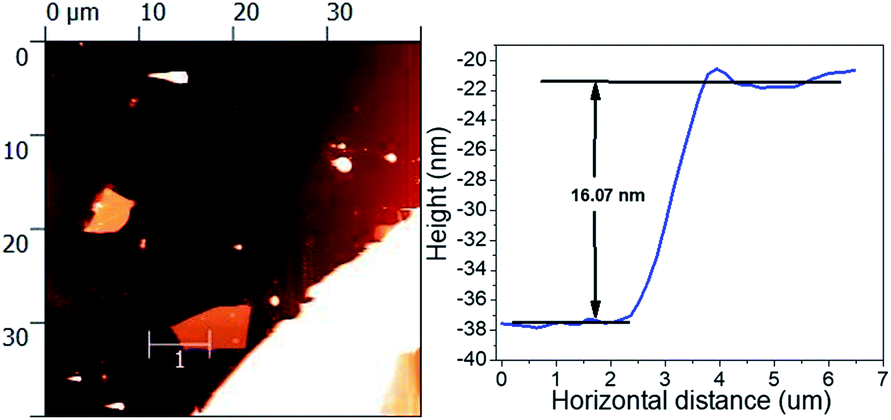 | ||
| Fig. 1 AFM image and the corresponding AFM height profile of the typical phosphorene nanosheet. | ||
Raman peaks are related to the in-plane (Ag2 and B2g) and out-of-plane (Ag1) vibrational modes. Probe power was found to be an important parameter herein. Powers in excess of 23 mW cm−2 were found to damage phosphorene, leading to peak position shifts, even with the passivation layers. Power densities in the range from 2 to 5 mW cm−2 were used to avoid the damage. The effect of annealing temperature on the Raman spectra is shown in Fig. 2(a–c) for Si3N4, Al2O3, and Al2O3/Si3N4 passivation layers, respectively. Raman spectroscopy was performed on the same sample in the as-deposited state (un-annealed) as well as after each step in a series of increasing temperature anneals from 100 °C to 600 °C. The sample with a Si3N4 passivation layer demonstrated clear phonon peaks of in-plane (Ag2 and B2g) and out-of-plane (Ag1) vibrational modes. Peak heights started to degrade at 450 °C, with visible peaks up to 550 °C annealing. In comparison, samples passivated by Al2O3 show degradation at temperature as low as 300 °C and also exhibit loss of peaks at 450 °C; samples with Al2O3/Si3N4 hybrid layers have intermediate results with degradation beginning at 400 °C and peaks persisting up to a 500 °C anneal.
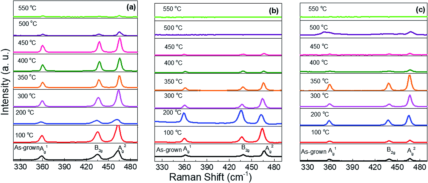 | ||
| Fig. 2 Raman spectra of the phosphorene/AZO samples passivated by (a) Si3N4, (b) Al2O3, and (c) Si3N4/Al2O3 layers, annealed at different temperatures. | ||
Shifts in the Raman peak position are typically attributed to the effect of stress. Blue shifts indicate increase in the compressive stress or decrease in the tensile stress. Phosphorene has a puckered honeycomb structure; thus, so biaxial strain can be present in both the zigzag and armchair directions.25 The peak positions are plotted in Fig. 3(a–c). To help evaluate this shift, the peak positions for a similar flake without a passivation layer are shown as a dashed line. The results obtained for the unannealed samples show the effect of the passivation layer stress on phosphorene; the out-of-plane mode shows that the effects of annealing is similar to that in the case of the in-plane peaks; the effects are less pronounced for in-plane peaks as can be expected.
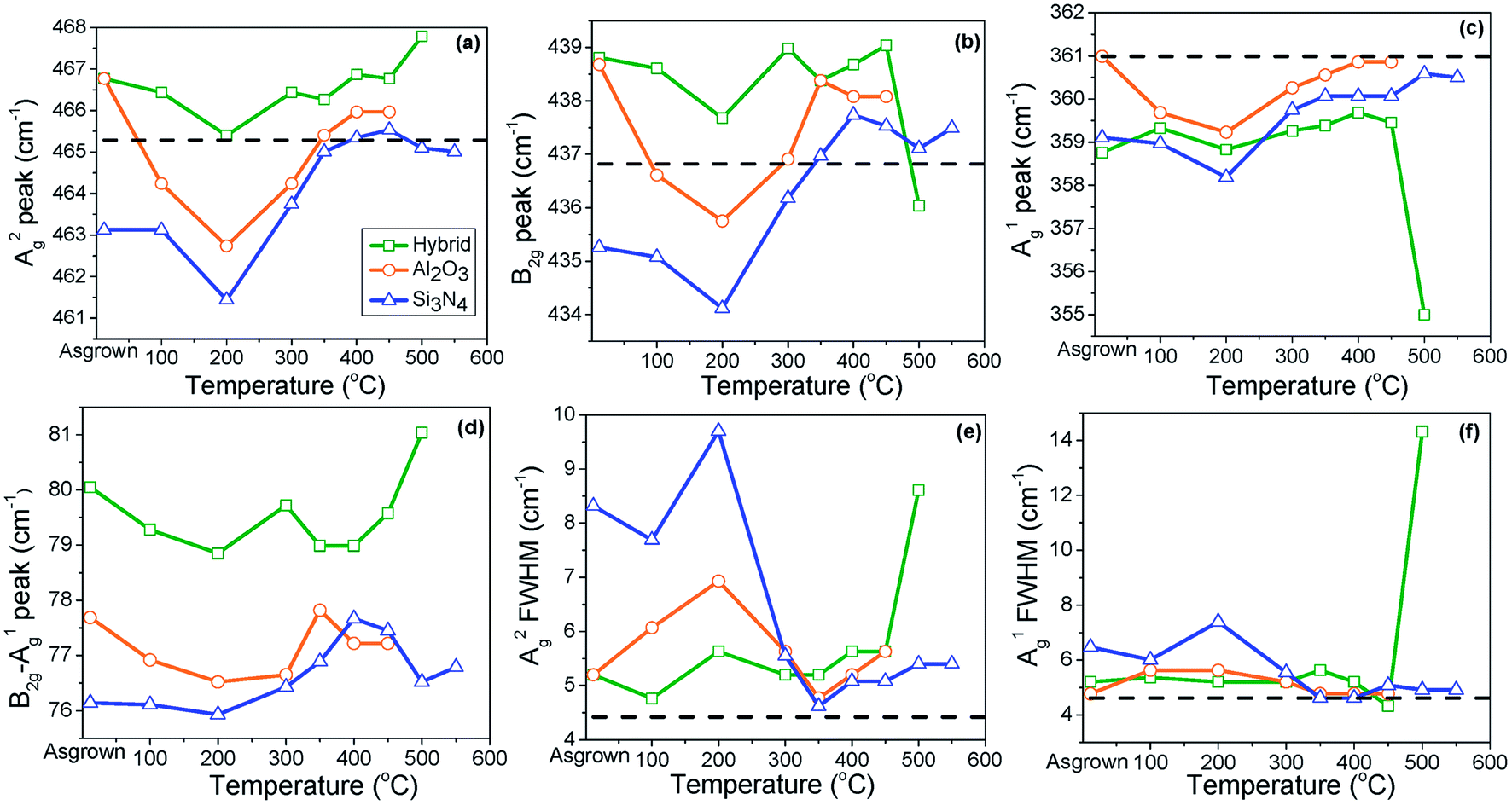 | ||
| Fig. 3 Raman shifts of (a) Ag2, (b) B2g, and (c) Ag1 vibrational modes at different annealing temperatures. (d) The delta Raman shift between B2g and Ag1 vibrational modes at different annealing temperatures. The full-width at half maximum (FWHM) variation of (e) Ag2 and (f) Ag1 phonon modes with annealing temperature for different samples. | ||
The annealing results can be divided into three regimes: a low temperature red shift, a medium temperature blue shift, and high temperature degradation. The red shift occurs for anneals up to 200 °C. It is especially pronounced for the Si3N4 passivated sample. The blue shift occurs between 200 and 400 °C anneals. Peak positions slightly change between 400 °C and 450 °C. The behavior of the samples for high temperature (>400 °C) anneals was strongly passivation dependent. As abovementioned, Al2O3 and Al2O3/Si3N4 samples did not show Raman peaks once annealed at 550 and 500 °C, respectively, due to deterioration of phosphorene. Peak positions were erratic at the highest anneal temperatures for each sample. Presumably, this was due to the extensive crystal degradation. The energy spacing between the Ag1 and B2g modes decreases when the material is stretched, but increases under compression.25 In our study, the energy spacing between Ag2 and B2g modes returns to its low temperature value at higher annealing temperatures for the Si3N4 passivated structure, as shown in Fig. 3(d). These observations differ from those reported in a previous study by Late, which indicated a linear red shift with the increasing temperatures up to 400 °C on a SiO2/Si substrate.26 This could be due to sample differences. In Late's report, no passivation layer was used on the phosphorene flakes; this allowed free expansion of phosphorene by annealing.26 The red shift in phosphorene is due to stretch in the zigzag direction.27 The energy spacing is higher for Al2O3 and Si3N4/Al2O3 passivation layers as compared to that for the Si3N4 passivation layer, as shown in Fig. 3(d). This indicates lower Raman peak intensities for Al2O3 and Si3N4/Al2O3 passivation layers as compared to those for the Si3N4 passivation layer.25
There are two possible reasons for the behavior observed in Fig. 3(a–d). The first is out-diffusion of Zn atoms from the AZO film. The atomic radius of the Zn atoms (1.42 Å) is larger than the radius of P atoms (0.98 Å). Thus, the incorporation of Zn in phosphorene can result in a lattice distortion, generating a compressive strain that compensates the already present tensile strain in phosphorene.22,26 Since diffusion coefficients increase exponentially with temperature, the amount of Zn incorporation into the phosphorene layer would increase sharply with annealing temperature. The second possible explanation is that the stress in the passivation layers is decreased by thermal annealing; this reduces the stress in phosphorene. To further study this, we deposited the passivation layers directly on 4′′ silicon wafers and used wafer bowing to determine the average film stress. We replicated the anneals applied to the phosphorene samples, and the stress after each anneal was measured. The results are shown in Fig. 4. Because the deposition was directly conducted on silicon rather than on the sample structure (phosphorene on AZO), the absolute values of the stress in these films may be different in this measurement. However, the annealing trends should show similar effects. Both films show a pronounced change in stress upon anneals of 300–450 °C. This effect has been reported elsewhere.28 It is believed to be due to a densification caused by the loss of hydrogen from the films. This leads to tensile strain in the passivation layer when it is deposited on conventional materials. When it is deposited on a 2D material, the weak inter-plane forces will permit significant strain relaxation, but some degree of tensile strain will still exist. Thus, the densification of the passivation layer leads to compressive strain in phosphorene, producing the blue shift observed in Fig. 3.
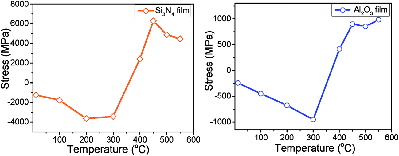 | ||
| Fig. 4 Stress in the passivation layers as a function of annealing temperature. | ||
It is tempting to ascribe the medium temperature shift in the Raman position (Fig. 2), which occurs from 200 to 400 °C, with this H2 loss in the passivation layers, but there is an apparent difference in temperature. However, there are a few reasons to be skeptical of this apparent temperature difference. As described in the methods section, the samples were annealed in an optically heated rapid thermal processing system. The observed temperature in this system is the read out for a thermocouple in contact with a 4′′ silicon wafer. For the work summarized in Fig. 4, this is the actual coated wafer, whereas the work described in Fig. 3 was conducted on small samples (∼1 cm2) that were placed on top of the monitored 4′′ silicon wafer in the RTP system. Poor thermal contact could be responsible for some of this difference. More significant, however, is the fact that we are heating optically. Phosphorene has a short absorption length in the optical region, and the thin layer provides a very small thermal mass.29 Therefore, it is possible that the temperature of phosphorene and adjacent passivation layer significantly exceeds the measured temperature during heating transients due to the poor thermal contact of the system.
The crystalline properties of phosphorene were also investigated for different annealing temperatures by calculating FWHM of Ag2 and Ag1 phonon peaks, as shown in Fig. 3(e and f), respectively. The FWHM of phonon peaks is a good indicator of the crystalline quality. It is noteworthy to mention that the heights of peaks decrease abruptly between 100 °C and 200 °C, as shown in Fig. 2(a). The highest decrement is observed for 200 °C annealing temperature. The FWHM values of these peaks are large for this temperature range (from as-grown to 200 °C), as shown in Fig. 3(e and f). This indicates that the quality of the phosphorene flake is low in this temperature range; this results in the lower heights of peaks. It was observed that annealing at 350 °C produced phonon peaks with a much lower FWHM. Measurements of bulk black phosphorus indicated a FWHM of about 5 cm−1, comparable to the annealing results. Nitride-passivated films show marginally better results than the other samples. The decomposition of the Al2O3/Si3N4 passivated structure at 500 °C is clearly visible in this plot. The return of the FWHM to the bulk value is an interesting result. If the strain relaxation was driven by the Zn up-diffusion, an increase in the in the peak width would be expected due to alloy broadening effects related to the disorder in the crystal. The fact that this was not seen suggested that this was not the case for our samples. The small FWHM in the high temperature-annealed Si3N4-coated samples strongly suggests that the nitride acts as a diffusion barrier for phosphorus, allowing the crystalline layer to not only remain intact but actually improve its crystallinity for anneals that would otherwise destroy the material through sublimation. The upper limit for this effect is not known, but is likely to exceed the maximum temperature of 550 °C studied herein.
Finally, we have investigated that why the Si3N4 passivation layer allows annealing at higher temperatures. Black phosphorus is known to be most stable of the various allotropes. However, it is also known to sublime at high temperatures. While the bulk material (black phosphorous) remains reasonably stable up to 550 °C, phosphorene degrades at temperatures as low as 400 °C, as noted by Liu.30 This is common for many nanostructures, including nanoparticles, nanotubes, and nanowires, and is believed to be due to the large surface to volume ratio. It is reasonable to suspect that the nitride layer acts as a diffusion barrier, blocking phosphorene decomposition by impeding the subliming flux of phosphorus atoms. Ito et al. studied the high temperature diffusion of phosphorus in thin nitride on top of silicon.31 For 30 minute anneals at 1000 °C, the dose of phosphorus in the wafer is reduced by three orders of magnitude for a 3.4 nm nitride and nearly five orders of magnitude for a 9.2 nm nitride layer as compared to that of a SiO2 layer. Since the dose is proportional to the flux, it is clear that at this temperature, nitride is an effective diffusion barrier. Caution should be exercised while extrapolating from processes occurring at 1000 °C to processes occurring under the conditions used here, but note that reduction in the temperature will only reduce the diffusion coefficient further and nitride deposited is amorphous; thus, there will be no grain boundary diffusion effect at low temperatures.
Fig. 5 shows the schematic of the fabricated phosphorene/AZO heterojunction p–n diode. Fig. 5(b) illustrates the current–voltage (I–V) characteristics of device measured at different annealing temperatures. To ensure that the diode represents the heterojunction and not a contact, resistors of both phosphorene and AZO with the same Ti/Au contacts were tested as well. These show low resistance ohmic behavior, as shown in Fig. 5(c). It is well known that AZO has n-type conductivity; this indicates the p-type nature of phosphorene. The forward bias ideality factor was determined after annealing at different temperatures, as shown in Fig. 5(d). The series resistance at 1.2 V dropped slightly with annealing, from 24 kΩ to 15 kΩ, suggesting an improvement in layer conductivity or a reduction in the contact resistance. The ideality factor decreased with an increase of annealing temperature; this indicated improved quality, achieving a minimum value of 3.3 after annealing at 500 °C (Fig. 5(d)). Rectifying I–V characteristics disappear and ohmic behavior is observed after annealing at 550 °C.
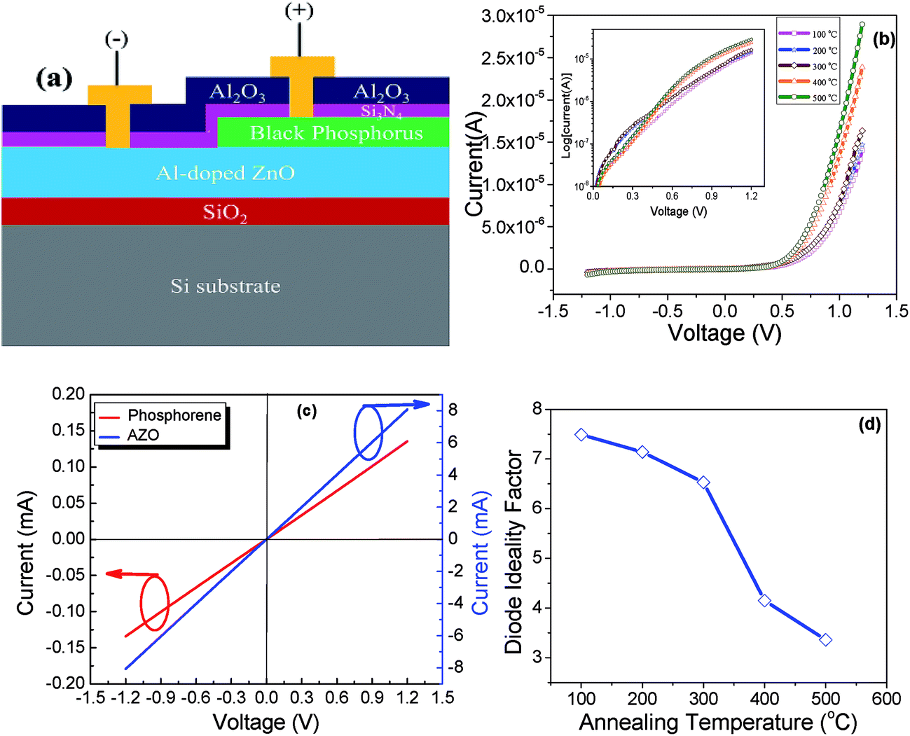 | ||
| Fig. 5 (a) Device structure. (b) I–V characteristics of the phosphorene/AZO heterojunction diode at different annealing temperatures. Inset shows the semilog scale. (c) I–V characteristics showing ohmic behavior by the Ti/Au contact on phosphorene and AZO layers. (d) Ideality factor versus annealing temperature. | ||
Annealing can have multiple effects including change in the conductivity of the films by changing the carrier concentration or mobility, change in the specific resistance of the contacts, and change in the defect density in the bulk or at the interface.19 The series resistance of the device can be inferred from the slope of the I–V characteristics at large forward bias. Herein, we see only a modest difference and thus rule out the first two possible effects. We, therefore, believe that annealing reduces the defect concentration and therefore the recombination current. This can be seen most easily in the small-value (100 mV to 300 mV) of forward bias characteristics shown in the inset of Fig. 5(b). A reduction of the current in this region, along with a drop in the ideality factor, is a clear indication that annealing is reducing the recombination rate. At higher bias values, carriers are injected from the n-region to the p-region and vice versa. Therefore, the current is due to the diffusion of carriers in the quasi-neutral regions. The diffusion coefficient improves after higher temperature annealing due to the reduction of the defect concentration. Perhaps more importantly, however, the forward current is proportional to exp(VA/nkT). As the ideality factor (n) decreases, the value of the exponent increases for a given applied voltage, and thus, the current increases exponentially. Raman measurements showed that the phosphorene crystalline quality was improved for anneals at higher temperature; this resulted in a reduction of the defect concentration. We cannot tell from this data if this improvement is at the interface or in the bulk. The loss of rectifying behavior after annealing at 550 °C corresponds to the reduction in the Raman peak intensities and the increase in the peak width for the nitride-passivated samples at this temperature. All these observations suggest a sharp drop in the crystal quality.
IV. Conclusions
Herein, three samples having a few-layer phosphorene/AZO heterostructure were passivated by Al2O3, Si3N4, and Al2O3/Si3N4 layers separately using PE-ALD. These phosphorene/AZO heterostructures were annealed at different temperatures, and the thermal stability was measured by Raman spectroscopy. AFM measurements confirmed that all samples had phosphorene flakes with thicknesses in the range of 8–16 nm. The Si3N4-passivated structure demonstrated highest thermal sustainability, showing clear vibrational modes for annealing temperature in the range of 100–550 °C. The phonon peaks red shifted after annealing up to 200 °C; this suggested the generation of tensile strain and/or reduction of compressive strain. For annealing temperatures above 200 °C, phosphorene produced a blue shift in the in-plane (B2g and Ag2) and out-of-plane (Ag1) vibrational modes, returning to the peak positions for the unannealed sample. Thus, strain relaxation took place at higher annealing temperature for the Si3N4 structure. We believe that the effect of annealing on the strain of the passivation layers plays a critical role in these shifts. The fabricated phosphorene/AZO heterojunction diode shows improvement in the quality of diode at higher annealing temperatures. Herein, we present a study that has the potential to accelerate further developments in the field of high-performance phosphorene/ZnO heterojunction-based wide-band devices such as photodetectors.Conflicts of interest
There are no conflicts to declare.Acknowledgements
Part of this work was carried out at the Nano Center of University of Minnesota, which was supported by the National Science Foundation through NNCI (Award ECCS-1542202). SKP and NI also received support through this award. We are also grateful to the atomic force microscopy (AFM) and Raman spectroscopy facilities equipped at the Characterization Facility at the University of Minnesota.References
- K. Kim, J. Y. Choi, T. Kim, S. H. Cho and H. J. Chung, Nature, 2011, 479, 338–344 CrossRef CAS PubMed.
- Q. H. Wang, K. K. Zadeh, A. Kis, J. N. Coleman and M. S. Strano, Nat. Nanotechnol., 2012, 7, 699–712 CrossRef CAS PubMed.
- F. H. L. Koppens, T. Mueller, P. Avouris, A. C. Ferrari, M. S. Vitiello and M. Polini, Nat. Nanotechnol., 2014, 9, 780–793 CrossRef CAS PubMed.
- F. Schwierz, Nat. Nanotechnol., 2010, 5, 487–496 CrossRef CAS PubMed.
- G. Fiori, F. Bonaccorso, G. Iannaccone, T. Palacios, D. Neumaier, A. Seabaugh, S. K. Banerjee and L. Colombo, Nat. Nanotechnol., 2014, 9, 768–779 CrossRef CAS PubMed.
- K. S. Novoselov, V. I. Fal’ko, L. Colombo, P. R. Gellert, M. G. Schwab and K. Kim, Nature, 2012, 490, 192–200 CrossRef CAS PubMed.
- P. Avouris, Z. Chen and V. Perebeinos, Nat. Nanotechnol., 2007, 2, 605–615 CrossRef CAS PubMed.
- M. K. Jana, A. Singh, D. J. Late, C. R. Rajamathi, K. Biswas, C. Felser, U. V. Waghmare and C. N. R. Rao, J. Phys.: Condens. Matter, 2015, 27, 285401 CrossRef PubMed.
- D. J. Late, S. N. Shirodkar, U. V. Waghmare, V. P. Dravid and C. N. Rao, ChemPhysChem, 2014, 15, 1592–1598 CrossRef CAS PubMed.
- L. Li, Y. Yu, G. J. Ye, Q. Ge, X. Ou, H. Wu, D. Feng, X. H. Chen and Y. Zhang, Nat. Nanotechnol., 2014, 9, 372–377 CrossRef CAS PubMed.
- Y. Cai, G. Zhang and Y. W. Zhang, Sci. Rep., 2014, 4, 6677–6683 CrossRef CAS PubMed.
- H. Liu, A. T. Neal, Z. Zhu, Z. Luo, X. Xu, D. Tomanek and P. D. Ye, ACS Nano, 2014, 8, 4033–4041 CrossRef CAS PubMed.
- H. Liu, Y. Du, Y. Deng and P. D. Ye, Chem. Soc. Rev., 2015, 44, 2732–2743 RSC.
- J. Dai and X. Zeng, J. Phys. Chem. Lett., 2014, 5, 1289–1293 CrossRef CAS PubMed.
- F. Xia, H. Wang, D. Xiao, M. Dubey and A. Ramasubramaniam, Nat. Photonics, 2014, 8, 899–907 CrossRef CAS.
- K. W. Ang, Z. P. Ling and J. Zhu, IEEE International Conference on Digital Signal Processing, 2015, p. 1223 Search PubMed.
- P. K. Kannan, D. J. Late, H. Morgan and C. S. Rout, Nanoscale, 2015, 7, 13293–13312 RSC.
- P. J. Jeon, Y. T. Lee, J. Y. Lim, J. S. Kim, D. K. Hwang and S. Im, Nano Lett., 2016, 16, 1293–1298 CrossRef CAS PubMed.
- Y. Deng, Z. Luo, N. J. Conrad, H. Liu, Y. Gong, S. Najmaei, P. M. Ajayan, J. Lou, X. Xu and P. D. Ye, ACS Nano, 2014, 8, 8292–8299 CrossRef CAS PubMed.
- P. Gehring, R. Urcuyo, D. L. Duong, M. Burghard and K. Kern, Appl. Phys. Lett., 2015, 106, 233110 CrossRef.
- S. K. Pandey, S. K. Pandey, C. Mukherjee, P. Mishra, M. Gupta, S. R. Barman, S. W. D'Souza and S. Mukherjee, J. Mater. Sci.: Mater. Electron., 2013, 24, 2541–2547 CrossRef CAS.
- S. K. Pandey, S. K. Pandey, U. P. Deshpande, V. Awathi, A. Kumar, M. Gupta and S. Mukherjee, Semicond. Sci. Technol., 2013, 28, 085014 CrossRef.
- S. J. Pearton, D. P. Norton, K. Ip, Y. W. Heo and T. Steiner, J. Vac. Sci. Technol., B: Microelectron. Nanometer Struct.--Process., Meas., Phenom., 2004, 22, 932–948 CrossRef CAS.
- M. Köpf, N. Eckstein, D. Pfister, C. Grotz, I. Krüger, M. Greiwe, T. Hansen, H. Kohlmann and T. Nilges, J. Cryst. Growth, 2014, 405, 6–17 CrossRef.
- R. Fei and L. Yang, Appl. Phys. Lett., 2014, 105, 083120 CrossRef.
- D. J. Late, ACS Appl. Mater. Interfaces, 2015, 7, 5857–5862 CAS.
- Z. P. Ling and K. W. Ang, APL Mater., 2015, 3, 126104 CrossRef.
- A. Bagolini, A. S. Savoia, A. Picciotto, M. Boscardin, P. Bellutti, N. Lamberti and G. Caliano, J. Micromech. Microeng., 2015, 25, 015012 CrossRef.
- S. Zhang, J. Yang, R. Xu, F. Wang, W. Li, M. Ghufran, Y. W. Zhang, Z. Yu, G. Zhang, Q. Qin and Y. Lu, ACS Nano, 2014, 8, 9590–9596 CrossRef CAS PubMed.
- X. Liu, J. D. Wood, K. S. Chen, E. K. Cho and M. C. Hersam, J. Phys. Chem. Lett., 2015, 6, 773–778 CrossRef CAS PubMed.
- T. Ito, S. Hijiya, T. Nozaki, H. Arakawa, M. Shinoda and Y. Fukukawa, J. Electrochem. Soc., 1978, 125, 448–452 CrossRef CAS.
| This journal is © The Royal Society of Chemistry 2017 |