
 Open Access Article
 This Open Access Article is licensed under a
 Creative Commons Attribution 3.0 Unported Licence
Investigation on the properties of Ta doped Ti3SiC2 as solid oxide fuel cell interconnects
Lili Zheng *ab,
Qingsong Huaa,
Xichao Li*bc,
Meishuan Lib,
Yuhai Qianb,
Jingjun Xub,
Zuoqiang Daia,
Tao Chena,
Jianmin Zhanga and
Hongxin Zhanga
*ab,
Qingsong Huaa,
Xichao Li*bc,
Meishuan Lib,
Yuhai Qianb,
Jingjun Xub,
Zuoqiang Daia,
Tao Chena,
Jianmin Zhanga and
Hongxin Zhanga
aPower & Energy Storage System Research Center, College of Mechanical & Electronic Engineering, Qingdao University, Qingdao, 266071, China
bShenyang National Laboratory for Materials Science, Institute of Metal Research, Chinese Academy of Sciences, Shenyang 110016, China
cQingdao Institute of Bioenergy and Bioprocess Technology, Chinese Academy of Sciences, Qingdao, 266101, China. E-mail: lixc@qibebt.ac.cn
First published on 1st September 2017
Abstract
The oxidation behaviours and electrical properties of 5 at% Ta doped Ti3SiC2 solid solution have been investigated at 800 °C in air for up to 500 h. The oxidation kinetics of (Ti0.95Ta0.05)3SiC2 follows a parabolic law. The oxidation rate constant is 7.33 × 10⁻¹⁴ g2 cm−4 s−1, which is lower than those of Ti3SiC2, (Ti0.95Nb0.05)3SiC2 and Crofer 22 APU. Ta doped r-TiO2 formed (Ti0.95Ta0.05)3SiC2 during the oxidation process. Ta doping can limit the outward diffusion of Ti by decreasing the native Ti interstitials concentration and simultaneously restraining the inward diffusion of oxygen by decreasing the O vacancy concentration. As a result, the oxidation resistance is significantly improved and the oxide scale structure of Ti3SiC2 changes from a double-layer to a monolithic layer. The ASR of (Ti0.95Ta0.05)3SiC2 after oxidation at 800 °C in air for 500 h is 29.5 mΩ cm2, which is much lower than that of Ti3SiC2. Ta doping can increase the electron concentration in r-TiO2 and thereby increase the electrical conductivity of r-TiO2. Therefore, the ASR of (Ti0.95Ta0.05)3SiC2 after oxidation is lower compared to that of Ti3SiC2.
1. Introduction
Due to concerns relating to the energy crisis and environmental deterioration, solid oxide fuel cells (SOFC), as one of the promising clean energy technologies, have drawn much attention. SOFC possesses many advantages, such as high efficiency, fuel flexibility, and low contribution towards pollution. It is an electrochemical device which generates electricity and heat from fuel and produces chemical energy without combustion.1,2 For SOFC commercialization, interconnects are an essential part. Interconnects are used to build up multiple cell-stacks from the single cell. It plays two roles: (1) acts as the physical separator of fuels in the anode cavity and air or oxygen in the cathode cavity; (2) acts as the bipolar plate electrically connecting adjacent cells in series.3 The requirements for interconnect materials are strict and include the following: good electrical conductivity; good oxidation, corrosion, and carburization resistance; adequate stability in terms of dimension, microstructure, chemistry and phase at operating temperature in oxidizing and reduction environments; gas tightness; appropriate thermal expansion coefficient, and no reaction and inter-diffusion with adjacent components.2–4 Over the past decades, LaCrO3 and doped LaCrO3 have been widely studied as interconnects for SOFC. However, there are many native defects, which hinder its extensive development, such as difficulty in sintering and machining of compact chromite parts and high manufacturing costs.2 As the working temperature of SOFC decreases to intermediate temperature (600–800 °C),5–7 metal becomes the main material used as the interconnect. Metallic interconnects have many advantages, such as high electrical and thermal conductivity, low cost, easy manufacture and good workability.8,9 However, all metallic interconnects have the “chromium oxide poison” problem. The main oxide formed on the metallic interconnect is Cr2O3. Cr species evaporation can poison the cathode and the cathode/electrolyte interface and result in the degradation of performance of SOFC.10 Also, the stepwise increase in area specific resistance (ASR) of surface scale hinders the development of metallic interconnects. To overcome these problems, various new kinds of alloys11–20 and coatings21–28 have been explored. However, these issues have not been completely resolved. Therefore, more efforts are needed to develop a novel Cr-free interconnect material. It should possess good oxidation resistance as well as post-oxidation superficial electrical conductivity.MAX phases are a group of layered ternary compounds, marked as Mn+1AXn (M: early transition metal, A: IIIA or IVA element, X: C and/or N). They have attracted significant attention due to the merits of both ceramics and metals. Ti3SiC2, one of the most typical MAXs, possesses unique properties, such as low density, high modulus and fracture toughness, high electrical and thermal conductivity, easy machinability, good resistance to oxidation and thermal shock below 1100 °C.29,30 However, the oxidation resistance of pure Ti3SiC2 at a working temperature cannot satisfy the requirements of interconnects. One of the most effective methods to improve the oxidation resistance of Ti3SiC2 is the substitution of a transition metal element for Ti. For example, our previous works31,32 show that the Nb doped Ti3SiC2 solid solutions significantly improve the oxidation resistance of Ti3SiC2. What's more, these solutions possess better oxidation resistance and lower ASR than two typical metallic interconnects, Crofer 22APU and E-brite. (Ti1−xNbx)3SiC2 is a great potential material in the application as an interconnect for IT-SOFC. After Nb doping, the oxidation rate of (Ti,Nb)3SiC2 decreases remarkably. The reduction concentration of oxygen vacancies and titanium interstitials in rutile TiO2 (r-TiO2) by Nb doping is the main reason. Interestingly, the post-oxidation ASR of (Ti,Nb)3SiC2 is also decreased greatly.31
As in the same transition element group with Nb, Ta ion also possesses penta-valence after ionization. The ionic radium for Ti4+, Nb5+, and Ta5+ is 0.068 nm, 0.069 nm, and 0.070 nm, respectively. The ionic radium difference of Ta with Ti is larger than that of Nb with Ti. It is reasonable to believe that Ta doped Ti3SiC2 may exhibit more suitable performance than Nb doped any other metallic interconnect. In this paper, the Ta doped Ti3SiC2 solution is successfully synthesized, and the oxidation behaviours and electrical property of this solid solution are investigated at 800 °C in air up to 500 h. We aim to not only explore a novel and promising interconnects for SOFC, but also study the effect mechanism of Ta on the oxidation behaviours and electrical property of Ti3SiC2.
2. Experimental
5 at% Ta doped Ti3SiC2 bulk material was fabricated by in situ solid–liquid reaction/hot pressing process. The raw powders of titanium, tantalum, silicon and graphite were selected at a molar ratio of 2.85![[thin space (1/6-em)]](https://www.rsc.org/images/entities/char_2009.gif) :0.15:1:2. The final solid solution was denoted as (Ti0.95Ta0.05)3SiC2 according to the nominal apportions of the raw powders. To avoid the appearance of a second phase of TiC, a little Al powder was also added to the raw powders. All raw powders were mixed and milled in a polypropylene jar for 24 h. After ball milling, the powders were cool pressed uniaxially under 5 MPa in a graphite die with a diameter of 50 mm. The in situ reaction/hot press sintering was carried out at 1580 °C under a pressure of 30 MPa for 1 h in flowing Ar atmosphere. The predominant phase for the as-synthesized solid solution was Ti3SiC2, and small quantities of (Ti,Ta)Si2 and (Ti,Ta)5Si2 impurities also appeared. Compared to that of pure Ti3SiC2, the peak corresponding to the (101) lattice plane of (Ti0.95Ta0.05)3SiC2 shifted to a lower angle (about 0.036°). It revealed that the rutile lattice parameter corresponding to (101) plane had increased. The EDS surface scanning on the (Ti0.95Ta0.05)3SiC2 crystal grain (not shown here for abbreviation) showed that Ta was in the grain, and the atomic ratio of Ta/(Ti + Ta) was about 5%. From the above results, it was deduced that Ta had been doped into Ti3SiC2 lattice, and the lattice parameter of Ti3SiC2 had been changed because Ta had a larger radius than Ti. The density of the solid solution was determined by the Archimedes method in which three parallel samples were tested to acquire the mean value. The density of this solid solution was 4.92 ± 0.02 g cm−3, and the relative density was ∼99.2%.
:0.15:1:2. The final solid solution was denoted as (Ti0.95Ta0.05)3SiC2 according to the nominal apportions of the raw powders. To avoid the appearance of a second phase of TiC, a little Al powder was also added to the raw powders. All raw powders were mixed and milled in a polypropylene jar for 24 h. After ball milling, the powders were cool pressed uniaxially under 5 MPa in a graphite die with a diameter of 50 mm. The in situ reaction/hot press sintering was carried out at 1580 °C under a pressure of 30 MPa for 1 h in flowing Ar atmosphere. The predominant phase for the as-synthesized solid solution was Ti3SiC2, and small quantities of (Ti,Ta)Si2 and (Ti,Ta)5Si2 impurities also appeared. Compared to that of pure Ti3SiC2, the peak corresponding to the (101) lattice plane of (Ti0.95Ta0.05)3SiC2 shifted to a lower angle (about 0.036°). It revealed that the rutile lattice parameter corresponding to (101) plane had increased. The EDS surface scanning on the (Ti0.95Ta0.05)3SiC2 crystal grain (not shown here for abbreviation) showed that Ta was in the grain, and the atomic ratio of Ta/(Ti + Ta) was about 5%. From the above results, it was deduced that Ta had been doped into Ti3SiC2 lattice, and the lattice parameter of Ti3SiC2 had been changed because Ta had a larger radius than Ti. The density of the solid solution was determined by the Archimedes method in which three parallel samples were tested to acquire the mean value. The density of this solid solution was 4.92 ± 0.02 g cm−3, and the relative density was ∼99.2%.
For oxidation tests, 10 × 10 × 2 mm square coupons were cut from the as-synthesized bulk by the electrical discharge method. Prior to oxidation, the surfaces of the samples were grounded down to 2000 SiC paper, chamfered, polished using 1 μm diamond paste, and then degreased in ethanol and distilled water.
Oxidation tests were carried out in a tube furnace at 800 °C in air for up to 500 h. In the whole oxidation period, the step sequence was as follows: (1) the samples were heated up to 800 °C with furnace heating; (2) after every 100 h of isothermal oxidation at 800 °C, the samples were cooled down rapidly to room temperature in air; (3) the samples were weighed using a microbalance with an accuracy of 1 × 10⁻⁵ g; (4) the samples were then put into the hot furnace again.
The oxidation products were identified by X-ray diffraction (XRD) in a D/max -2500PC diffractometer (Rigaku, Tokyo, Japan) with Cu Kα radiation. The morphologies of the surface and the cross-section of the oxide scale formed on the matrix were observed by the SUPRA35 scanning electron microscope (SEM, LEO, Oberkochen, Germany). This SEM is equipped with an energy-dispersive spectroscopy (EDS, INCA, Oxford Instrument, Oxford, U.K.) system. Before SEM examination, a thin layer of Au was evaporated on the surface of the oxidized sample.
The electrical conductivity of (Ti0.95Ta0.05)3SiC2 after oxidation was determined by the 2-probe 4-point method in static air. The ASR was adopted to evaluate the electrical property of the oxidized coupons. ASR can reflect the integrated effect of both electrical resistivity and thickness of the oxide scale. To ensure the tight surface contact, Pt mesh was used, and Pt-paste was applied as a high temperature conductive adhesive. A constant current with 10 mA was supplied by the Precision Programmable Current Source (YL4012), and the corresponding voltage drop was recorded continuously by the FLUKE 8845A 6-1/2 Digit Programmable Multimeter.
3. Results and discussion
3.1 Oxidation behaviour
| (Δw/A)2 = kpt | (1) |
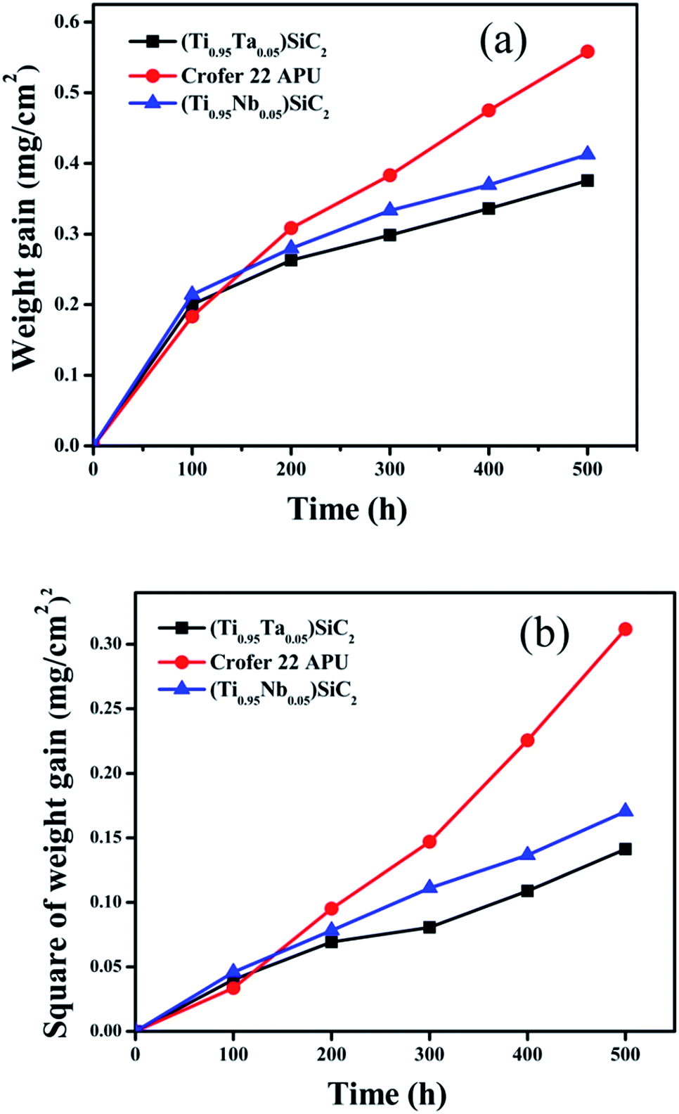 | ||
| Fig. 1 Weight gain per unit area vs. time (a) and square of weight gain per unit area vs. time (b) of (Ti0.95Ta0.05)3SiC2, (Ti0.95Nb0.05)3SiC2 and Crofer 22 APU at 800 °C in air. | ||
| Material | Mass gain after 500 h oxidation (g cm−2) | kp (g2 cm−4 s−1) |
|---|---|---|
| Ti3SiC2 | 1.01 | 5.64 × 10⁻¹³ |
| (Ti0.95Ta0.05)3SiC2 | 0.38 | 7.33 × 10⁻¹⁴ |
| (Ti0.95Nb0.05)3SiC2 | 0.41 | 9.18 × 10⁻¹⁴ |
| Crofer 22 APU | 0.56 | 1.71 × 10⁻¹³ |
From Table 1, it can be seen that after Ta doping, the oxidation resistance of Ti3SiC2 is improved. And its oxidation rate constant is decreased by approximate one order of magnitude than that of Ti3SiC2. Compared with Nb doping, Ta doping exhibits a better effect on improving the oxidation resistance of Ti3SiC2.
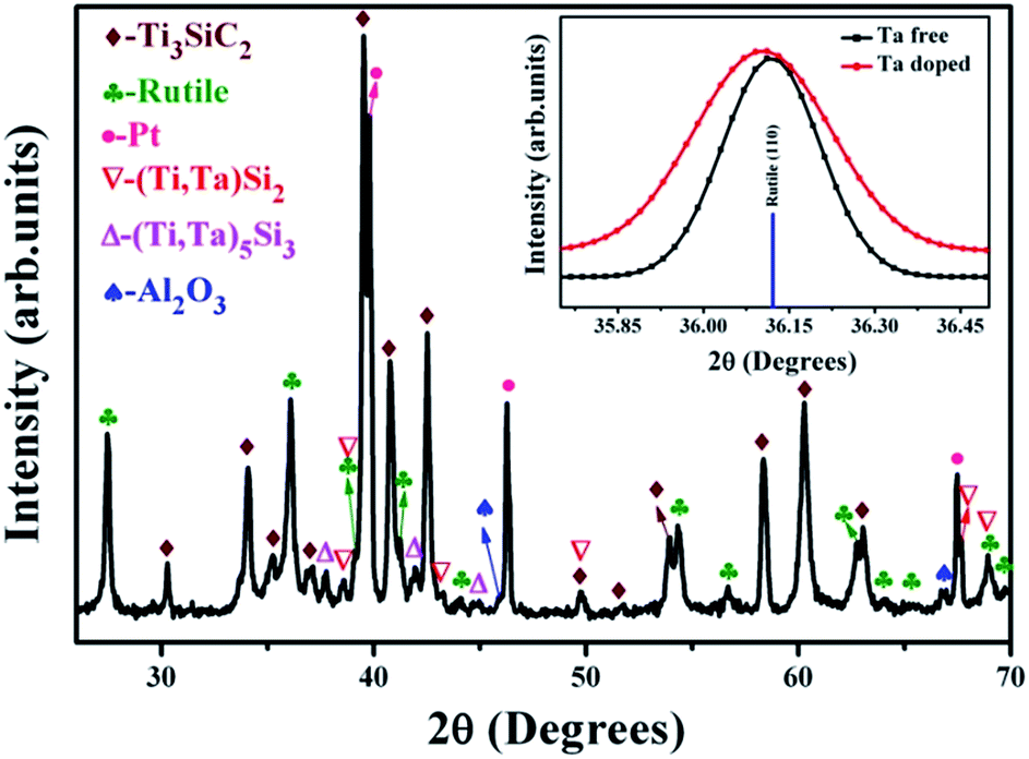 | ||
| Fig. 2 XRD pattern of (Ti0.95Ta0.05)3SiC2 after oxidation at 800 °C in air for 500 hours; the inserted figure is comparison of (101) peak position of r-TiO2 formed on (Ti0.95Ta0.05)3SiC2 and Ti3SiC2 after oxidation at 800 °C in air for 500 hours. | ||
Fig. 3 exhibits the surface morphologies of (Ti0.95Ta0.05)3SiC2 after oxidation. The contour of the substrate is clearly visible, which indicates that the oxide scale is very thin. This is in accordance with the XRD results. Meanwhile, some abnormal areas exist on the surface marked in the rectangular portion in Fig. 3. It is the oxide scale formed on (Ti,Ta)Si2 and (Ti,Ta)5Si2 identified by EDS (the EDS results are not shown here for abbreviate). These impurities possess different oxidation rates from that of the matrix phase, leading to the rough surface on the oxidized sample.
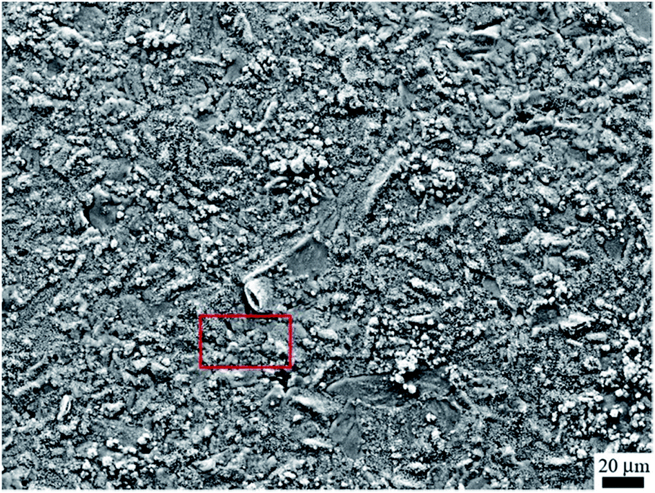 | ||
| Fig. 3 Surface morphology of (Ti0.95Ta0.05)3SiC2 after oxidation at 800 °C in air for 500 hours. | ||
Fig. 4 illustrates the cross-section morphology of the oxide scales formed on (Ti0.95Ta0.05)3SiC2 and corresponding with EDS elements line-scanning profiles along the red line. It clearly shows that the oxide scale formed on (Ti0.95Ta0.05)3SiC2 is a monolithic layer, and the thickness is approximate 3 μm. No void or local spallation is found at the oxide/substrate interface, implying good adherence between the oxide monolithic layer and the substrate. The samples have experienced five thermal cycles from room temperature to 800 °C in air. The fine interface can avoid electron scattering and allows for electron transportation through the interface. From the EDS line scanning, it can be known that the monolithic oxide layer is rich in Ti, Si, O and shows traces of Ta. Because the content is negligible, Al is not detected. Ti and Ta elements are distributed uniformly in the oxide layer. For Si, however, a higher content is found near the substrate than near the outer surface of the oxide layer. While a notable amount of Si element is detected in the oxide layer, no Si-containing oxide is identified by XRD. Therefore, it can be deduced that SiO2 exists in an amorphous form in the oxide layer. The formation of amorphous SiO2 has also been found during the oxidation of Ti3SiC2,34–37 Ti5Si3,38 MoSi2,39 and Si3N4.40 Therefore, it can be concluded that the single oxide layer consists of a mixture of Ta doped r-TiO2, amorphous SiO2 and a little of Al2O3. The previous works31 present that the oxide scale formed on Ti3SiC2 is composed of a double-layer and the thickness of the oxide layers is about 7 μm. The above results reveal that like Nb, Ta addition can also enhance the oxidation resistance of Ti3SiC2 and change the oxide layer structure from a duplex-layer to a monolithic layer structure. In addition, it is found that the morphology of plate-like grain in the matrix is clearly visible, which reveals that the (Ti0.95Ta0.05)3SiC2 structure is stable without phase and grain morphology change.
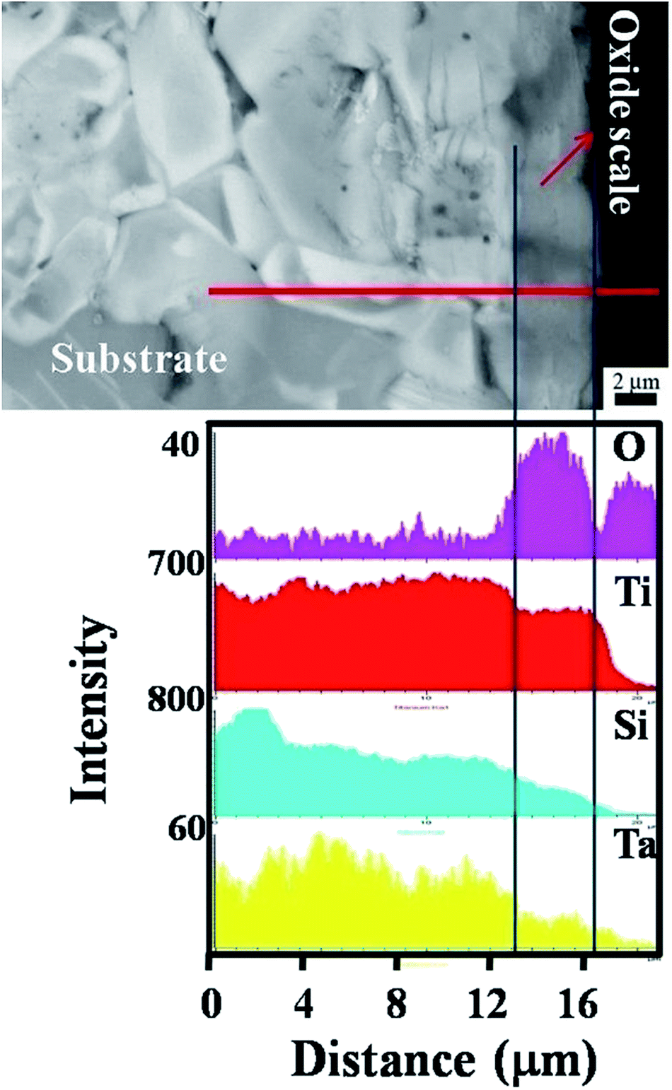 | ||
| Fig. 4 Cross-section morphology and EDS line scanning taken across the oxide scale formed on (Ti0.95Ta0.05)3SiC2 after oxidation at 800 °C in air for 500 hours. | ||
3.2 Electrical conductivity
The electrical conductivity of the interconnect under the SOFC atmosphere is significant, because the interconnect electrically connects adjacent cells. Like metallic interconnects, (Ti0.95Nb0.05)3SiC2 and Ti3SiC2, the substrates of (Ti0.95Ta0.05)3SiC2 ceramics, have much higher electrical conductivity than its corresponding oxide scales even at 800 °C.41 Therefore, the electrical resistance of (Ti0.95Ta0.05)3SiC2 after oxidation is mainly contributed from the oxide scale formed on the surface. Fig. 5 presents the ASR of (Ti0.95Ta0.05)3SiC2 after oxidation at 800 °C in air for 500 h. For comparison, the results for (Ti0.95Nb0.05)3SiC2, Ebrite and Crofer 22 APU33 are also presented. It can be seen that the curve for (Ti0.95Ta0.05)3SiC2 is in agreement with a line law, and the slope of the curve changes at 700 °C. When the temperature is higher than 600 °C and 650 °C, the ASR of (Ti0.95Ta0.05)3SiC2 is larger than that of Ebrite and Crofer 22 APU, respectively. The main oxide formed on Crofer 22 APU is Cr2O3. As the electrical resistance vs. temperature of Cr2O3 nearly obeys the line law, it is deduced that the ASR of (Ti0.95Ta0.05)3SiC2 after oxidation is smaller than that of Ebrite and Crofer 22 APU below 600 °C and 650 °C, respectively. It is suggested that the electrical conductivity of (Ti0.95Ta0.05)3SiC2 as an interconnect is better than Ebrite and Crofer 22 APU when SOFC service temperature is lower than 600 °C and 650 °C, respectively. The ASR of (Ti0.95Ta0.05)3SiC2 is larger than that of (Ti0.95Nb0.05)3SiC2 in the temperature range of 500–800 °C. The Ta doping effect on reducing ASR for the oxide scale is not as good as that of Nb. It may be caused by the higher electrical resistance of Ta doped TiO2 than that of the Nb doped one.42 The ASR of (Ti0.95Ta0.05)3SiC2 at 800 °C after oxidation at the same temperature in air for 500 h is 29.5 mΩ cm2, which is lower than that of Ti3SiC2 (85.0 mΩ cm2) treated under the same conditions for 20 h. This suggests that Ta addition greatly improved the electrical conductivity of post-oxidized Ti3SiC2.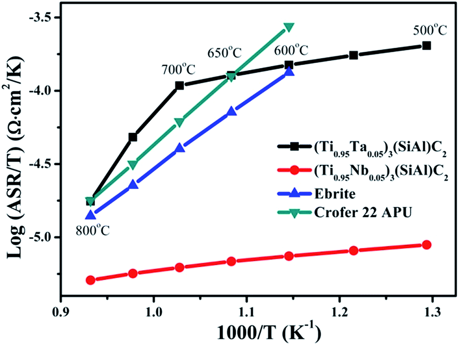 | ||
| Fig. 5 Temperature dependencies of ASR of (Ti0.95Ta0.05)3SiC2, (Ti0.95Nb0.05)3SiC2, Ebrite, and Crofer 22 APU after oxidation at 800 °C in air. | ||
3.3 Mechanism of Ta doping effect
From the previous results, it is known that after Ta doping, the oxidation resistance of Ti3SiC2 is enhanced and becomes even better than that of Nb. Furthermore, after Ta doping, the oxide scale layer of Ti3SiC2 is changed from a duplex-layer to a monolithic layer of Ta doped r-TiO2, amorphous SiO2 and a small amount of Al2O3.The oxygen diffusion coefficient of TiO2 and the electronic conductivity of TiO2 are much higher than those of SiO2. The oxidation of (Ti0.95Ta0.05)3SiC2 is controlled by the diffusion of ions though the oxide scale. The ion diffusion through the oxide scale, especially through the lattice of TiO2, is the control step. For the electrical conductivity of the oxidized (Ti0.95Ta0.05)3SiC2, the ASR depends on the formed oxide scale (r-TiO2 and amorphous SiO2), which especially depends on the electron diffusion through the r-TiO2. Therefore, it is deduced that Ta addition increases the oxidation resistance and the electrical conductivity of Ti3SiC2 after oxidation, mainly by affecting the transmission of ions and electrons through r-TiO2.
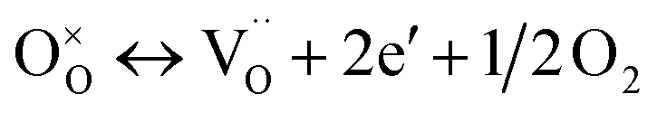
TiO2 is an n-type semiconductor and oxygen vacancies, tri- and quadri-valent Ti interstitials exist as native defects. When penta-valent Ta ions are doped into r-TiO2 lattice, the donation energy level of Ta produces an energy band. According to the defect chemistry theory, the following defect chemistry reaction will be proposed in an air atmosphere43–45 (expressed as Kröger and Vink's defect symbols46,47):
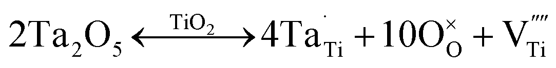 | (2) |
This means that after Ta is doped into the r-TiO2 lattice, the vacancy of Ti is produced. As there are oxygen vacancies, tri- and quadri-valent Ti interstitials in the r-TiO2 lattice, after the vacancy of Ti is generated, the following equilibrium will take place:
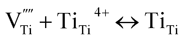 | (3) |
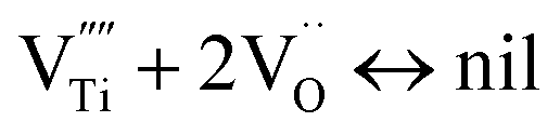 | (4) |
Furthermore, the following reaction will happen after reaction (4):
 | (5) |
The equilibrium constant of reaction (5) can be expressed as:
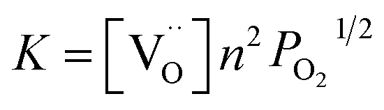 | (6) |
The above equilibriums (3) and (4) mean that after vacancy of Ti is produced, the Ti interstitial and oxygen vacancy will react with the vacancy of Ti. This will lead to a decrease in the concentration of Ti interstitial as well as oxygen vacancy in r-TiO2. Therefore, it is deduced that Ta doping decreases the outward diffusion of Ti by decreasing the concentration of native Ti interstitials and simultaneously restraining the inward diffusion of oxygen by decreasing the concentration of O vacancies. As a result, after Ta doping in Ti3SiC2, the oxidation resistance of Ti3SiC2 enhances remarkably, the oxidation rate constant decreases about one order of magnitude, and the oxide structure changes from a duplex-layer to a single mixture layer.
At the same time, when reaction (4) happens, the 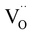 decreases. Then, according to equilibrium (6), the electron concentration of “n” in r-TiO2 correspondingly increases. This means that the electrical conductivity of the Ta doped TiO2 will increase. This can be the main reason for the lower ASR of (Ti0.95Ta0.05)3SiC2 after oxidation compared to that of the un-doped Ti3SiC2.
4. Conclusions
The oxidation behaviours and electrical property of 5 at% Ta doped Ti3SiC2 solid solution has been investigated at 800 °C in air up to 500 h. The following conclusions are drawn:(1) The oxidation kinetics of (Ti0.95Ta0.05)3SiC2 follows parabolic law, and the oxidation rate constant is 7.33 × 10⁻¹⁴ g2 cm−4 s−1, which is lower than that of Ti3SiC2, (Ti0.95Nb0.05)3SiC2 and Crofer 22 APU.
(2) The ASR of (Ti0.95Ta0.05)3SiC2 at 800 °C after oxidation at 800 °C in air for 500 h is 29.5 mΩ cm2, which is much lower than that of Ti3SiC2. Ta addition greatly improved the electrical conductivity of Ti3SiC2 after oxidation. The ASR of (Ti0.95Ta0.05)3SiC2 will be smaller than that of Ebrite and Crofer 22 APU when the temperature is lower than 600 °C and 650 °C, respectively.
(3) Ta doping can decrease the outward diffusion of Ti by decreasing the concentration of native Ti interstitials. Meanwhile, this restrains the inward diffusion of oxygen by decreasing the concentration of O vacancies. This results in the enhanced oxidation resistance of Ti3SiC2 and the changed oxide layer structure from a double-layer to a single mixture layer.
(4) The increased concentration of electrons in r-TiO2 by Ta doping results in increased electrical conductivity of the –TiO2. This is the main reason for the lower ASR of (Ti0.95Ta0.05)3SiC2 after oxidation compared to that of Ti3SiC2.
Conflicts of interest
There are no conflicts to declare.Acknowledgements
This work was financially supported by the National Science Foundation of China (Grant No. 51271191, 51571205 and 41406106), and the Scientific Research Start-up Fund of Qingdao University (Grant No. 41117010089).Notes and references
- N. Q. Minh, J. Am. Ceram. Soc., 1993, 76, 563 CrossRef CAS.
- J. W. Fergus, Mater. Sci. Eng., A, 2005, 397, 271 CrossRef.
- Z. G. Yang, K. S. Weil, D. M. Paxton and J. W. Stevenson, J. Electrochem. Soc., 2003, 150(9), A1188 CrossRef CAS.
- W. Z. Zhu and S. C. Deevi, Mater. Sci. Eng., A, 2003, 348, 227 CrossRef.
- T. Ishihara, H. Matsuda and Y. Takita, J. Am. Chem. Soc., 1994, 116, 3801 CrossRef CAS.
- S. D. Souza, S. J. Visco and L. C. D. Jonghe, J. Electrochem. Soc., 1997, 144, L35 CrossRef.
- P. Huang and A. Petric, J. Electrochem. Soc., 1996, 143, 1644 CrossRef CAS.
- M. Dokiya, Solid State Ionics, 2002, 152, 383 CrossRef.
- M. F. Han, S. Peng, Z. Wang, Z. Yang and X. Chen, J. Power Sources, 2007, 164, 278 CrossRef CAS.
- S. P. S. Badwal, R. Deller, K. Foger, Y. Ramprakash and J. P. Zhang, Solid State Ionics, 1997, 99, 297 CrossRef CAS.
- K. H. Joa, J. H. Kimb, K. M. Kimb, I. S. Leec and S. J. Kim, Int. J. Hydrogen Energy, 2015, 40, 9523 CrossRef.
- Z. G. Yang, M. S. Walker, P. Singh, J. W. Stevenson and T. Norby, J. Electrochem. Soc., 2004, 151(12), B669 CrossRef CAS.
- R. Sachitanand, M. Sattari, J. E. Svensson and J. Froitzheim, Int. J. Hydrogen Energy, 2013, 38, 15328 CrossRef CAS.
- S. J. Geng, J. H. Zhu and Z. G. Lu, Solid State Ionics, 2006, 177, 559 CrossRef CAS.
- P. Piccardo, S. Anelli, V. Bongiorno, R. Spotorno, L. Repetto and P. Girardon, Int. J. Hydrogen Energy, 2015, 40, 3726 CrossRef CAS.
- J. Froitzheim, G. H. Meier, L. Niewolak, P. J. Ennis, H. Hattendorf, L. Singheiser and W. J. Quadakkers, J. Power Sources, 2008, 178, 163 CrossRef CAS.
- B. Hua, J. Pu, F. S. Lu, J. F. Zhang, B. Chi and L. Jian, J. Power Sources, 2010, 195, 2782 CrossRef CAS.
- S. Swaminathan, Y. S. Lee and D. I. Kim, J. Power Sources, 2016, 327, 104 CrossRef CAS.
- P. D. Jablonski and D. E. Alman, J. Power Sources, 2008, 180, 433 CrossRef CAS.
- S. J. Geng, J. H. Zhu, M. P. Brady, H. U. Anderson, X. D. Zhou and Z. G. Yang, J. Power Sources, 2007, 172, 775 CrossRef CAS.
- B. K. Park, D. W. Kim, R. H. Song, S. B. Lee, T. H. Lim, S. J. Park, C. O. Park and J. W. Lee, J. Power Sources, 2015, 300, 318 CrossRef CAS.
- W. J. Shong, C. K. Liu, S. H. Wua, H. C. Liu and P. Yang, Int. J. Hydrogen Energy, 2014, 39, 19737 CrossRef CAS.
- X. N. Hosseini, M. H. Abbasi, F. Karimzadeh and G. M. Choi, J. Power Sources, 2015, 273, 1073 CrossRef.
- J. G. Grolig, P. Alnegren, J. Froitzheim and J. E. Svensson, J. Power Sources, 2015, 297, 534 CrossRef CAS.
- Z. G. Yang, G. G. Xi and J. W. Stevenson, Electrochem. Solid-State Lett., 2005, 8(3), A168 CrossRef CAS.
- A. Harthoj, T. Holt and P. Møller, J. Power Sources, 2015, 281, 227 CrossRef.
- A. M. Ruiz, K. Vidal, A. Larrañaga, J. M. P. Vázquez, P. R. Slater and M. I. Arriortua, Int. J. Hydrogen Energy, 2015, 40, 8407 CrossRef.
- N. Shaigana, W. Qua, D. G. Iveyb and W. X. Chen, J. Power Sources, 2010, 195, 1529 CrossRef.
- M. W. Barsoum and T. El-Raghy, J. Am. Ceram. Soc., 1996, 79, 1953 CrossRef CAS.
- Y. C. Zhou and Z. M. Sun, Mater. Res. Innovations, 1999, 2, 360 CrossRef CAS.
- L. L. Zheng, X. C. Li, Q. S. Hua, Z. Q. Dai, T. Z. Zhang, Y. H. Qian, J. J. Xu and M. S. Li, J. Am. Ceram. Soc., 2017, 100, 1 CrossRef.
- L. L. Zheng, J. J. Li, M. S. Li and Y. C. Zhou, Int. J. Hydrogen Energy, 2012, 37, 1084 CrossRef CAS.
- S. J. Geng, J. H. Zhu and Z. G. Lu, Scr. Mater., 2006, 55, 239 CrossRef CAS.
- Z. M. Sun, Y. C. Zhou and M. S. Li, Corros. Sci., 2001, 43, 1095 CrossRef CAS.
- Z. M. Sun, Y. C. Zhou and M. S. Li, Acta Mater., 2001, 49, 4347 CrossRef CAS.
- M. W. Barsoum, T. El-Raghy and L. U. J. T. Ogbuji, J. Electrochem. Soc., 1997, 144, 2508 CrossRef CAS.
- C. Racault, F. Langlais and R. Naslain, J. Mater. Sci., 1994, 29, 3384 CrossRef CAS.
- H. Jiang, C. S. Petersson and M. A. Nicolet, Thin Solid Films, 1986, 140, 115 CrossRef CAS.
- C. G. Mckamey, P. F. Tortorelli, J. H. DeVan and C. A. Carmichael, J. Mater. Res., 1992, 7, 2747 CrossRef CAS.
- Y. G. Gogotsi and F. Porz, Corros. Sci., 1992, 33, 627 CrossRef CAS.
- M. W. Barsoum, Prog. Solid State Chem., 2000, 28, 201 CrossRef CAS.
- D. M. Chen, G. Xu, L. Miao, S. Nakao and P. Jin, Surf. Coat. Technol., 2011, 206, 1020 CrossRef CAS.
- T. Bak, J. Nowotny, M. Rekas and C. C. Sorrell, J. Phys. Chem. Solids, 2003, 64, 1043 CrossRef CAS.
- T. Bak, J. Nowotny, M. Rekas and C. C. Sorrell, J. Phys. Chem. Solids, 2003, 64, 1057 CrossRef CAS.
- T. Bak, J. Nowotny, M. Rekas and C. C. Sorrell, J. Phys. Chem. Solids, 2003, 64, 1069 CrossRef CAS.
- F. A. Kröger and H. J. Vink, Solid State Phys., 1956, 3, 307 Search PubMed.
- M. F. Yan and W. W. Rhodes, Additives and interfaces in electronic ceramics, in Advances in Ceramics, ed. M. F. Yan and A. H. Heuer, American Ceramic Society, Columbus, OH, 1983, pp. 226–238 Search PubMed.
| This journal is © The Royal Society of Chemistry 2017 |