
 Open Access Article
 This Open Access Article is licensed under a Creative Commons Attribution-Non Commercial 3.0 Unported Licence
Enhanced light out-coupling efficiency and reduced efficiency roll-off in phosphorescent OLEDs with a spontaneously distributed embossed structure formed by a spin-coating method
Shuqing Yuana,
Yuying Hao *a,
Yanqin Miaob,
Qinjun Suna,
Zhanfeng Lia,
Yanxia Cuia,
Hua Wangb and
Bingshe Xub
*a,
Yanqin Miaob,
Qinjun Suna,
Zhanfeng Lia,
Yanxia Cuia,
Hua Wangb and
Bingshe Xub
aKey Lab of Advanced Transducers and Intelligent Control System of Ministry of Education, College of Physics and Optoelectronics, Taiyuan University of Technology, Taiyuan 030024, China. E-mail: haoyuyinghyy@sina.com
bKey Laboratory of Interface Science and Engineering in Advanced Materials, Taiyuan University of Technology, Taiyuan 030024, China
First published on 12th September 2017
Abstract
A simple and low-cost spin-coating method was proposed to form a spontaneously distributed embossed structure. With such an embossed structure produced by Al2O3 nanospheres (NPs) with different diameters, the out-coupling efficiency is increased in all viewing directions without introducing significant spectral changes and the efficiency roll-off is suppressed at the same time. When the concentration of Al2O3 ethanol solution is chosen as 0.08 mg ml−1, a peak current efficiency (CE) of 52.1 cd A−1, peak power efficiency (PE) of 32.7 l m W−1, and peak external quantum efficiency (EQE) of 20.9% are obtained. From the maximum efficiency value to the case where the brightness is 3000 cd m−2, the roll-off of CE, PE and EQE for device B are only 6.53%, 26.30% and 6.22%, respectively. The improved properties are attributed to greatly enhanced light extraction and an enlarged charge carrier recombination region.
1. Introduction
OLEDs hold great promise for both large area displays and lighting due to their excellent light-emitting performance.1–9 Especially, phosphorescent OLEDs (PHOLEDs) have received considerable attention compared with fluorescent OLEDs, owing to their almost 100% internal quantum efficiency (IQE) by efficiently utilizing both singlet and triplet excitons.1 However, one of the major drawbacks of conventional OLEDs is poor light extraction efficiency. Although the IQE of PHOLEDs can be close to 100%, their maximum EQE is only 20%,10–12 as a large proportion of spontaneous emission is trapped as different kinds of optical modes within the device,13–17 e.g., the substrate mode due to total internal reflection (TIR) caused by the mismatch of refractive indices between air (n = 1) and glass substrate (n = 1.5), the waveguide mode for the TIR at the glass/ITO layer (n ≈ 1.9) interface, or surface plasmon polariton (SPP) mode on the metal surface.Therefore, many methods have been done around increasing the out-coupling efficiency of OLEDs, including: using microlens array,18–20 large half sphere lens,21 surface roughness at the glass/air interface,22 periodic photonic crystal,23–25 microcavity OLEDs,26–28 high index substrates,29 metal free OLED,30 and spontaneously formed buckles.31–34 Among all these techniques, introducing spontaneously formed buckles in OLEDs have been proved to be an effective approach because of the enhanced light extraction without introducing spectral changes and directionality. This means the color gamut does not alter along the viewing direction, which is important for information displays.
However, the spontaneously formed buckles were usually fabricated by the techniques such as multiplexing light interference32 or nano-imprinting,33,34 which require more complicated and expensive fabrication processes and thus are not cost-effective for commercial applications. Thus, further studies are still required to increase out-coupling efficiency without spectral changes through a simple and cost-effective process.
In this letter, a randomly distributed scattering structure was developed by a simple low-cost solution based method. Herein the Al2O3 ethanol solution was spin-coated on the annealed PEDOT:PSS/ITO/glass film, then randomly placed Al2O3 NPs were obtained as a single layer. All the function layers deposited on Al2O3 NPs single layer were conformably patterned in such an OLED. Some substrate, waveguide and SPP modes which are confined in flat device can be extracted out into the air by such an embossed structure with color stability over all viewing angles. As a result, the prominent enhancement of 52.3%, 94.6%, and 52.6% in peak CE, PE, and EQE is achieved and the efficiency roll-off is improved relative to the planar device. We have attributed this effect to the enlarged charge carrier recombination region and decreased triplet exciton density. This method is expected to be useful for low-cost, large scale manufacturing of PHOLEDs with high efficiency and low efficiency roll-off.
2. Experimental
2.1 Preparation of embossed PHOLED using Al2O3 NPs
Fig. 1(a) shows the schematic diagram of the embossed PHOLED. The proposed embossed PHOLED has the structure of ITO/PEDOT:PSS/Al2O3 NPs/NPB (30 nm)/CBP:6 wt% Ir(ppy)3 (30 nm)/Bphen (40 nm)/LiF (1 nm)/Al (150 nm), where PEDOT:PSS [poly(3,4-ethylenedioxythiophene):polystyrenesulfonate] is used as the hole injection layer, NPB [N,N′-bis(naphthalen-1-yl)-N,N′-bis(phenyl)benzidine] as hole-transport-layer (HTL), CBP [4,4′-bis(carbazol-9-yl)-biphenyl] as the host of emitting layer (EML), Ir(ppy)3 [tris(2-phenylpyridine) iridium(III)] as phosphorescent dopant, Bphen [4,7-diphenyl-1,10-phenanthroline] as hole blocking layer (HBL) and electron transporting layer (ETL), respectively. | ||
| Fig. 1 The schematic diagrams of (a) the embossed PHOLED and (b) the planar PHOLED. | ||
The PEDOT:PSS aqueous solution was commercially purchased from Heraeus with concentration of 1 g ml−1. Al2O3 NPs powder was purchased from Shanghai ST-nano Science & Technology Co., Ltd. The mean diameters of the received Al2O3 NPs are 300 and 500 nm, respectively. These two kinds of Al2O3 NPs were firstly mixed according to the weight ratio of 1![[thin space (1/6-em)]](https://www.rsc.org/images/entities/char_2009.gif) :1, and then diluted with ethanol. The resulting concentrations of Al2O3 in ethanol solution are 0.2, 0.08 and 0.04 mg ml−1 for devices A, B and C, respectively, which is the only difference among the three devices. Other organic materials were purchased from Nichem Fine Technology Co., Ltd., and all materials were used as received.
:1, and then diluted with ethanol. The resulting concentrations of Al2O3 in ethanol solution are 0.2, 0.08 and 0.04 mg ml−1 for devices A, B and C, respectively, which is the only difference among the three devices. Other organic materials were purchased from Nichem Fine Technology Co., Ltd., and all materials were used as received.
The preparation process of embossed PHOLEDs is as follows. Glass substrates coated by indium tin oxide (ITO) with a sheet resistance of 10 Ω sq−1 were pre-cleaned in turn by ultrasonic treatment in deionized water and acetone, and then treated by UV ozone for 15 min. Subsequently, aqueous solution of PEDOT:PSS was spin-coated onto ITO at the spin rate of 3000 rpm for 60 s, then annealed at 120 °C for 15 min in the air ambient. Continuously, the Al2O3 ethanol solution after being stirred for 4 h at the temperature of 60 °C was spin-coated at the spin rate of 3000 rpm for 60 s on the annealed PEDOT:PSS films, then randomly placed Al2O3 NPs were obtained as a single layer. The following layers, including 30 nm-thick NPB, 30 nm-thick CBP:Ir(ppy)3, 40 nm-thick Bphen, 1 nm-thick LiF, and 150 nm-thick Al were in turn deposited on randomly placed Al2O3 NPs layer using thermal evaporation in high vacuum system with base pressure <5 × 10⁻⁴ Pa at deposition rates of 0.1 nm s−1 for organic materials, 0.01 nm s−1 for LiF and 0.5 nm s−1 for Al, respectively. The doped layers were performed by co-evaporating host and dopant loaded in the separate heating sources. The thickness and the evaporating rate of individual layers were monitored by quartz crystal monitors, which have been cross-calibrated with ellipsometry measurements for ensuring high accuracy.
For comparison, a planar structure named device D was designed and prepared, of which Al2O3 NPs layer was free, which was the only difference between the planar and the embossed structure. The schematic diagram of the planar PHOLED is shown in Fig. 1(b).
2.2 Characterization
The scanning electron microscopy (SEM) images of the emitting layer were investigated by SEM/FIB Crossbeam Workstation LYRA 3 XMH. The luminance–current–voltage (L–C–V) characteristics of the devices were measured by KEITHLEY 2400 and ST-900 M. The transmission spectra were measured by Shimadzu UV-2600 UV-vis spectrophotometer. The electroluminescent (EL) and photoluminescent (PL) spectra were recorded by SpectraScan PR 655 and Fluoromax-4 spectrophotometer, respectively. All the measurements were carried out at room temperature under ambient conditions.3. Results and discussion
The SEM image of the surface of the embossed CBP:Ir(ppy)3 EML based on Al2O3 NPs is shown in Fig. 2(a). For comparison, the SEM image of the planar CBP:Ir(ppy)3 EML is also given in Fig. 2(b). It can be seen clearly from Fig. 2(a) that on the surface of CBP:Ir(ppy)3/NPB/Al2O3 NPs/PEDOT:PSS/ITO/glass film, there are many randomly distributed globular bulges with different diameters induced by Al2O3 nanoparticles embedded in the bottom of NPB layer. In contrast, the surface morphology of CBP:Ir(ppy)3/NPB/PEDOT:PSS/ITO/glass film without Al2O3 NPs in Fig. 2(b) is extremely smooth.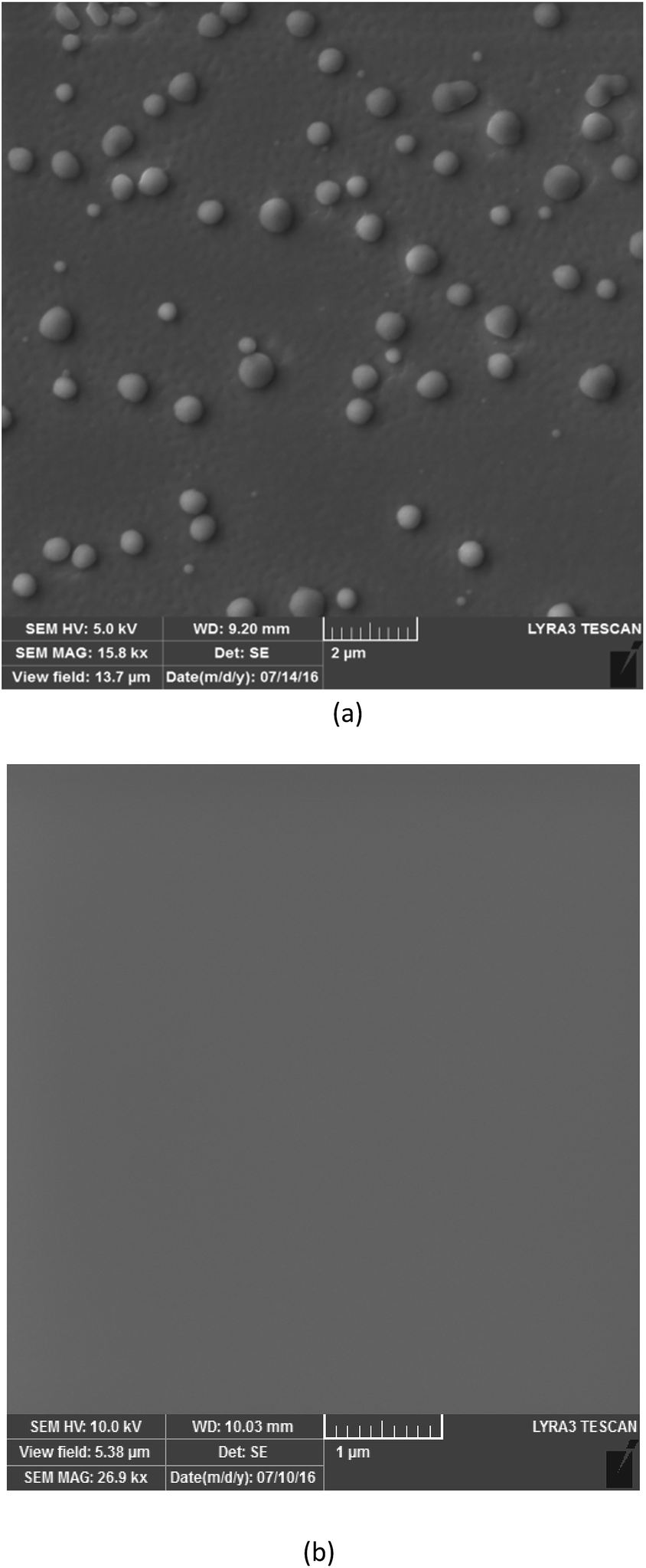 | ||
| Fig. 2 SEM images of the surfaces of (a) the embossed CBP:Ir(ppy)3 EML based on Al2O3 NPs, and (b) the planar CBP:Ir(ppy)3 EML. | ||
Fig. 3(a) shows the current density versus voltage characteristics of all devices. It is observed that the driving voltages of devices A–D at current density of 100 mA cm−2 are 6.5, 7.8, 8.5 and 11.5 V, respectively. This means all embossed devices have much lower driving voltages than planar one at the same current density. What's more, the driving voltages of the embossed devices decrease with the increase of the concentration of Al2O3 NPs solution. The driving voltage of device A was the lowest among all the devices, as seen in Fig. 3(a), in spite of the largest amount of insulating Al2O3 NPs. The distinctly lower driving voltage of device A may result from the partially reduced organic layer thicknesses and the enhanced electric field just because the structural change by the introduce of Al2O3 NPs.34–37 To verify this conclusion, we fabricated another device named device E with the same structure with device D except thinner thickness of NPB layer (15 nm). The current density–voltage characteristics of devices D and E are shown in Fig. 3(b). It can be seen clearly that the driving voltage of device E is obviously lower than that of device D at the same current density, which proves that the reduced organic layer thickness can cause remarkably decrease in device driving voltage.
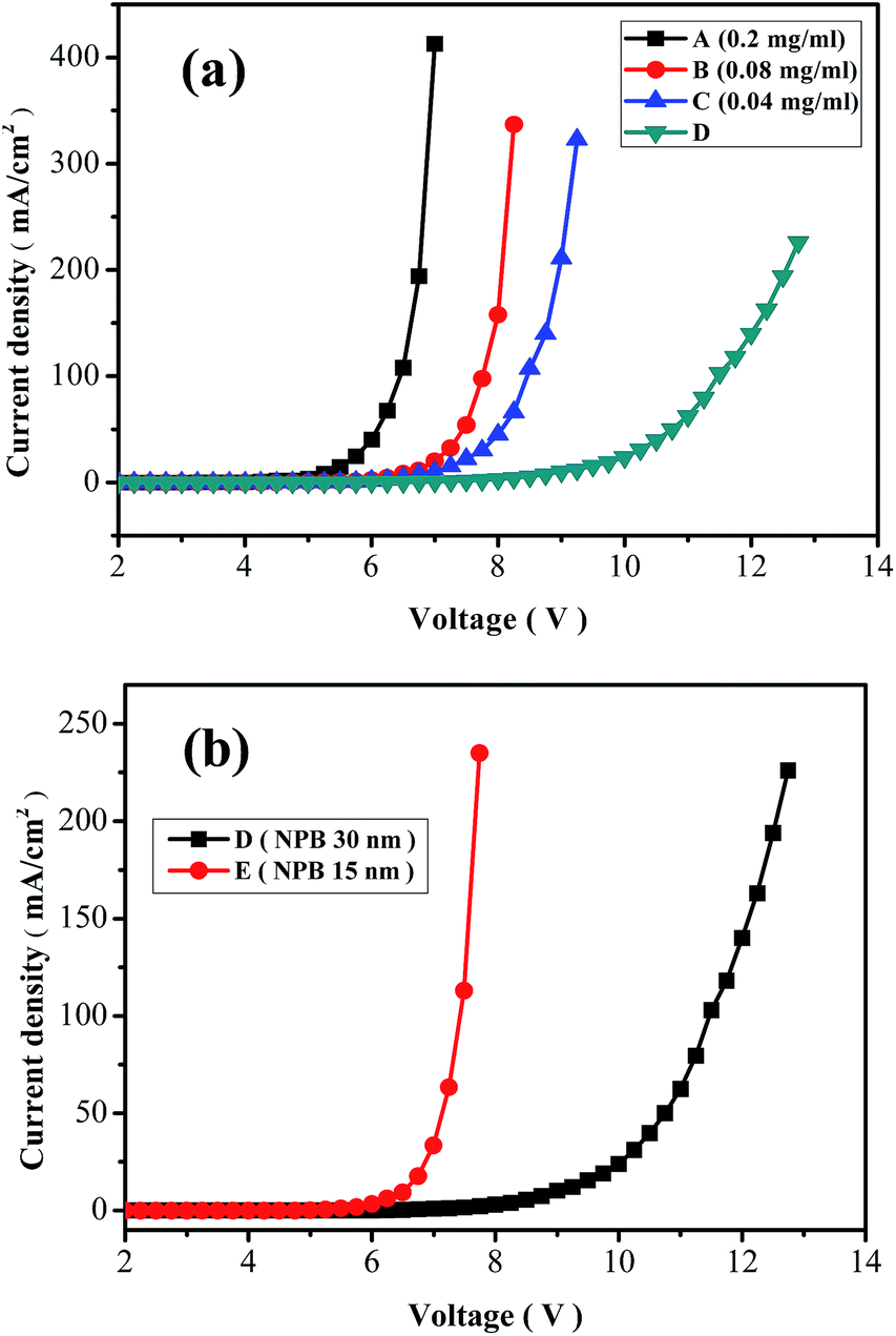 | ||
| Fig. 3 Current density–voltage characteristics of (a) devices A–D, and (b) devices D and E. | ||
The luminance versus current density curves of all devices are shown in Fig. 4. At a constant current density of 100 mA cm−2, the luminance of devices A–D is 34520, 38571, 31324 and 24126 cd m−2, respectively. And the maximum brightness for devices A–D is 130868, 123316, 90035 and 40600 cd m−2, respectively. That means the embossed PHOLEDs with Al2O3 film show more superior performance compared with the traditional planar device. Among them, the luminance of device B is the highest during all current density regions.
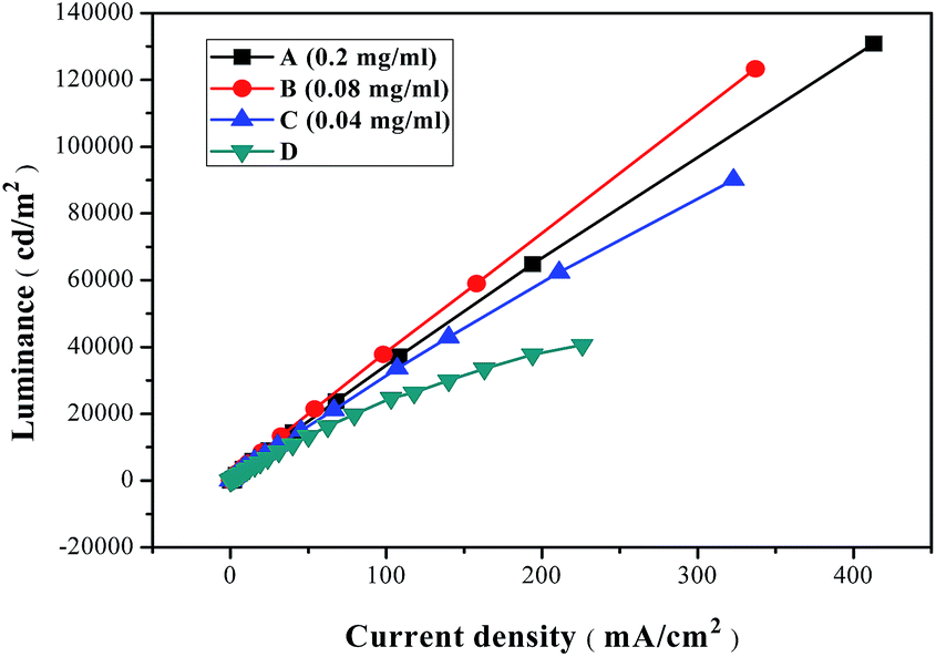 | ||
| Fig. 4 Luminance–current density characteristics of devices A–D. | ||
Fig. 5 shows the CE, PE and EQE of devices A–D. The details of the efficiency performances of all devices are summarized in Table 1. It is observed that the devices containing Al2O3 NPs have higher efficiencies compared with the planar device D under the same luminance. In particular, device B with the concentration of Al2O3 NPs of 0.08 mg ml−1 has the highest CE, PE and EQE among all the four devices. Compared with device D, device B exhibits a peak CE of 52.1 cd A−1 with the enhancement factor of 52.3%, a peak PE of 32.7 lm W−1 with the enhancement factor of 94.6%, and a peak EQE of 20.9% with the enhancement factor of 52.6%. What's more, the CE, PE and EQE values of the embossed devices keep at a significantly high level over all the observed luminance range. For example, the roll-off of CE, PE and EQE from the maximum efficiency value to the case at the brightness of 3000 cd m−2 for device B are 6.53%, 26.30% and 6.22%, respectively, while for device D the corresponding roll-off are 12.87%, 38.10% and 12.41% respectively, which are 1.97, 1.45 and 1.99 times those of device B. In a word, compared with the planar device D, the embossed devices show not only higher efficiencies but also lower efficiency roll-off. Although the PE of device B is slightly lower than that of device A as the luminance increases owing to slightly higher working voltages, the performance of device B is still considered as the most outstanding one among all devices, considering CE and EQE profile.
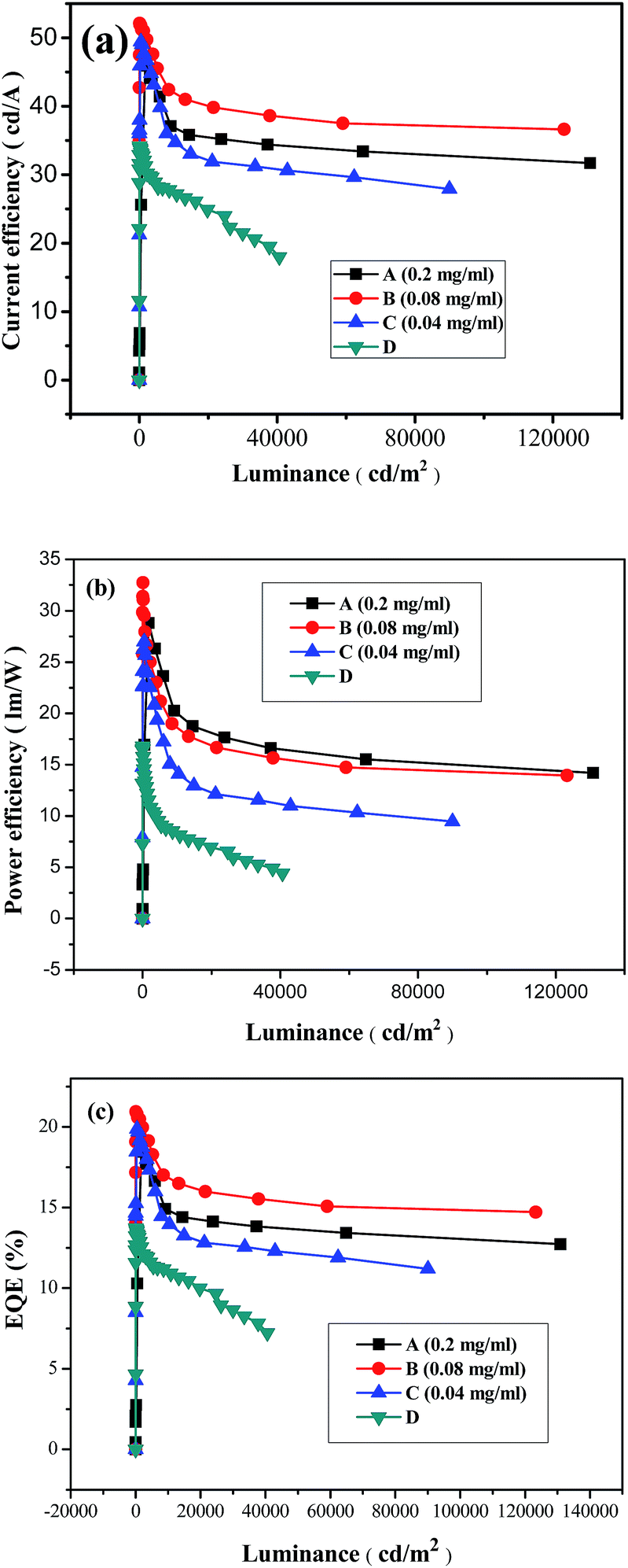 | ||
| Fig. 5 Efficiency performances of the embossed and planar PHOLEDs: (a) CE–luminance, (b) PE–luminance, and (c) EQE–luminance characteristics of devices A–D. | ||
| Device | CE (cd A−1) | PE (lm W−1) | EQE (%) | |||
|---|---|---|---|---|---|---|
| Max. | @3000 cd m−2 | Max. | @3000 cd m−2 | Max. | @3000 cd m−2 | |
| A | 46.0 | 44.6 | 28.8 | 27.1 | 18.4 | 17.9 |
| B | 52.1 | 48.7 | 32.7 | 24.1 | 20.9 | 19.6 |
| C | 49.4 | 45.6 | 27.0 | 21.6 | 19.9 | 18.3 |
| D | 34.2 | 29.8 | 16.8 | 10.4 | 13.7 | 12.0 |
In addition, it is noted that NPB is not optimized as the hole transporting layer in our devices, due to its lower triplet energy (2.29 eV) than that of the Ir(ppy)3 (2.42 eV), which easily lead to quenching of the excitons formed in Ir(ppy)3 by energy transfer to NPB. When a hole transporting material with higher triplet energy than that of Ir(ppy)3 is used, such as PHCZ2,38 the performance of our proposed device will be more excellent. For all that, the utilization of NPB still does not cover up the advantage of our proposed structure.
The remarkable performance improvement of the embossed devices is contributed by several factors. First, it is considered that the concave–convex structure formed by Al2O3 NPs actually shortens the organic layer thicknesses, enhances the electric field, which improves the hole and electron injection and transportation. Next, the concave–convex structure will broaden the charge carrier recombination region, which avoids exciton accumulation, decreases the triplet exciton density, and suppresses triplet exciton annihilation (TTA) and triplet-polaron annihilation (TPA), and then leads to the increase of efficiency and the reduction of efficiency roll-off in the embossed devices. Finally, the introduce of Al2O3 NPs and the conformably patterned function layers deposited on randomly placed Al2O3 NPs layer can intensify light out-coupling, and extrate more photons out of the embossed devices which are confined by substrate, waveguide and SPP modes in the planar one. Compared with device B, the slightly lower efficiencies of device A originate from the high concentration of Al2O3 NPs which could cause more non-radiative traps and phosphorescence quenching centers, and thus poor device performances. As for device C, the concentration of Al2O3 NPs is too low to form enough concave–convex profiles, so the light extraction and roll-off suppression effects are not as good as device B.
To further confirm the enhancement effect of light extraction by Al2O3 NPs, a concave–convex film with the structure of glass/ITO/PEDOT:PSS/Al2O3 NPs and a planar film with the structure of glass/ITO/PEDOT:PSS were prepared, respectively. All PEDOT:PSS films were formed by the same method with the PHOLEDs mentioned before (spin-coated, 3000 rpm for 60 s, and annealed, 120 °C for 15 min), and the concentration of Al2O3 NPs is 0.08 mg ml−1, the same with device B. The UV-vis transmission spectra of the two films are shown in Fig. 6(a). One can see clearly that the transmission of the concave–convex film is higher than that of the planar one at all wavelengths, which means when light is incident from the Al2O3 NPs layer, more light will be extracted into the air from the glass layer. This is attributed to the enhanced extraction of waveguide modes at the ITO/glass interface and substrate mode at the glass/air interface by the light scattering effect of Al2O3 NPs [Fig. 6(b)]. In addition, all functional layers such as EML and Al cathode layers in the embossed device are modulated into concave–convex profiles, therefore, the photons trapped in waveguide mode by TIR at PEDOT:PSS/NPB interface for the great difference of refractive indices between PEDOT:PSS (n = 1.48) and NPB (n = 1.79) and the photons lost as SPP mode on the metal surface in planar device can be extracted out as well. As a result, randomly arranged patterns of the embossed devices can enhance the out-coupling of substrate, waveguide and SPP modes.
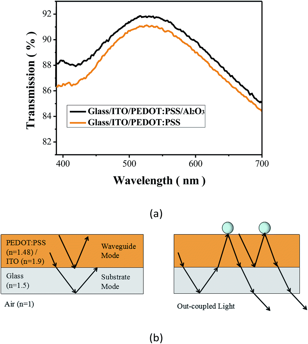 | ||
| Fig. 6 (a) Transmission spectra of the concave–convex film with the structure of glass/ITO/PEDOT:PSS/Al2O3 NPs and the planar film with the structure of glass/ITO/PEDOT:PSS. (b) Schematic diagram of waveguide and substrate mode losses in planar film (left) and light extraction in concave–convex film (right), and the refractive index n is also shown in the diagram. | ||
Next, we investigated the luminescence spectra of the embossed device B and the planar device D. Fig. 7(a) shows the EL spectra for the two PHOLEDs measured at the surface normal direction at a voltage of 7 V. The enhancement of EL intensity in the device with Al2O3 NPs over the reference one is caused by two reasons. Firstly, the current density of the embossed device is higher than that of the planar one under the same voltage, and the luminance will increase with the increase of current density. Secondly, the luminance of the embossed device is higher than that of the planar one under the same current density for the enhancement of light out-coupling and the reduction of triplet exciton quenching. Fig. 7(b) shows that the shape of the normalized EL emission spectrum of the embossed device is very similar to that of the planar one. The viewing angle dependence of EL intensity is shown in Fig. 7(c) and color coordinates are shown in Fig. 7(d). Fig. 7(c) presents the integration of EL spectra of device B and D over the entire wavelength region from 380 to 780 nm for the emission angles from 0° to 60° with 10° step and the data were normalized with the integration value of the EL spectra of planar device D in the surface normal direction. One can see that both embossed and planar PHOLEDs show a maximum EL intensity in the normal direction, the emission intensities of the embossed device B are greater than those of the planar one at all angles, and both the emission intensities of the two devices are almost identical to the Lambertian emission pattern, which mean that the luminous intensity of the embossed device is enhanced without angular dependence. Additionally, Fig. 7(d) shows the CIE color coordinates do not change significantly for all viewing angles. The CIE indices of the embossed device in the normal direction are (0.2933, 0.6221), which are similar to those of the planar one (0.2908, 0.6242). The CIE indices of the embossed device vary within Δx = 6.0% and Δy = 0.8% from 0° to 60° and those of the planar one show similar variations of Δx = 8.0% and Δy = 1.9%. And the product of the variation of CIE indices, |Δx × Δy|, is under 0.0001 for the embossed device, and 0.0003 for the planer one [see the inset of Fig. 7(d)], which confirms that the embossed structure improve the light out-coupling without significant spectral changes. This quite uniform enhancement of light extraction over all the emission wavelengths from 380–780 nm is attributed to broadly and randomly distributed Al2O3 NPs. Similarly, the improved extraction of optical modes is also reflected in PL emission of concave–convex film, shown in Fig. 8(a). One can see from Fig. 8(a) the PL spectrum of the embossed film is obviously stronger than that of the planar one. The normalized PL emission spectra of the two films are almost identical. This result, similar to that of EL spectra, further shows that the embossed structure can enhance light extraction over all visible spectra.
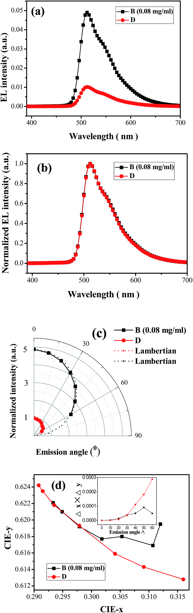 | ||
| Fig. 7 Luminescence spectral characteristics: (a) EL spectra of embossed and planar PHOLEDs measured at the surface normal direction at a voltage of 7 V. (b) Normalized EL spectra. (c) Viewing angle dependence of EL intensity for the embossed PHOLED (device B, black squares) and planar PHOLED (device D, red circles), normalized with the intensity of planar device in the surface normal direction, and the dashed lines represent the ideal Lambertian emission pattern. Both embossed and planar PHOLEDs show a maximum EL intensity in the normal direction and the emission intensities of the two devices are almost identical to the Lambertian emission pattern. (d) The CIE color coordinates for the emission angles from 0° to 60° with 10° step. Inset of (d): the product of the variation of CIE indices, |Δx × Δy|, at different emission angles. | ||
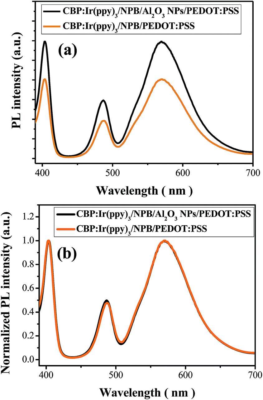 | ||
| Fig. 8 (a) PL spectra and (b) normalized PL spectra of the patterned CBP:Ir(ppy)3/NPB/Al2O3 NPs/PEDOT:PSS and the planar CBP:Ir(ppy)3/NPB/PEDOT:PSS films. | ||
4. Conclusions
In summary, we have introduced an extremely simple and effective spin-coating method to form spontaneously distributed buckling structures. The results indicate that the randomly embedded Al2O3 NPs used in PHOLEDs can decrease device driving voltages, enlarge charge carrier recombination region, decrease the triplet exciton density, and suppresses triplet exciton quenching. What's more, it can also enhance the out-coupling of substrate, waveguide and SPP modes in all viewing direction without introducing significant spectral changes. As a result, the embossed devices exhibit the best current efficiency of 52.1 cd A−1, power efficiency of 32.7 lm W−1, and EQE of 20.9%, which are 1.52, 1.95 and 1.53 times those of the reference device. Besides, the embossed devices also exhibit suppressed efficiency roll-off. The roll-off of CE, PE and EQE from the maximum efficiency value to the case at the brightness of 3000 cd m−2 are 6.53%, 26.30% and 6.22%, respectively, which are just 50.72%, 69.04% and 50.13% of those of the reference device. We conclude that such a low-cost and easy of large-scale fabrication method to form spontaneously distributed embossed structure fabricated simply by spin-coating can be used to increase the out-coupling efficiency and decrease efficiency roll-off, which could have important applications in high-performance displays and broad spectrum lighting.Conflicts of interest
There are no conflicts to declare.Acknowledgements
This research work was financially supported by National Natural Science Foundation of China (61274056, 61475109 and 61275037), Key Research and Development (International Cooperation) Program of Shanxi (201603D421042), and Platform and Base Special Project of Shanxi (201605D131038). Y. Cui acknowledges the Young Talents Program and Young Sanjin Scholars Program of Shanxi Province.References
- C. Adachi, M. A. Baldo, M. E. Thompson and S. R. Forrest, J. Appl. Phys., 2001, 90, 5048 CrossRef CAS.
- M. A. Baldo, D. O'brien, Y. You, A. Shoustikov, S. Sibley, M. Thompson and S. Forrest, Nature, 1998, 395, 151 CrossRef CAS.
- B. W. D'Andrade and S. R. Forrest, Adv. Mater., 2004, 16, 1585 CrossRef.
- Y. Li, Y. Hao, W. Li, S. Yuan, H. Liu, Y. Cui, H. Wang, B. Xu and W. Huang, Opt. Express, 2013, 21, 17020 CrossRef PubMed.
- S. Yuan, Y. Hao, Y. Miao, Q. Sun, Z. Li, Y. Cui, H. Wang, F. Shi and B. Xu, RSC Adv., 2015, 5, 89041 RSC.
- Q. Yang, Y. Hao, Z. Wang, Y. Li, H. Wang and B. Xu, Synth. Met., 2012, 162, 398 CrossRef CAS.
- Y. H. Yunfei Li, Z. Yan, H. Liu, H. Wang and B. Xu, Synth. Met., 2013, 164, 12 CrossRef.
- Y. Miao, X. Du, H. Wang, H. Liu, H. Jia, B. Xu, Y. Hao, X. Liu, W. Li and W. Huang, RSC Adv., 2015, 5, 4261 RSC.
- Y. Miao, Z. Gao, Y. Li, A. Zhang, H. Wang, Y. Hao, H. Jia, X. Liu and B. Xu, Synth. Met., 2015, 203, 59 CrossRef CAS.
- S. Reineke, F. Lindner, G. Schwartz, N. Seidler, K. Walzer, B. Lussem and K. Leo, Nature, 2009, 459, 234 CrossRef CAS PubMed.
- L. H. Smith, J. A. E. Wasey and W. L. Barnes, Appl. Phys. Lett., 2004, 84, 2986 CrossRef CAS.
- H. Uoyama, K. Goushi, K. Shizu, H. Nomura and C. Adachi, Nature, 2012, 492, 234 CrossRef CAS PubMed.
- W. Brütting, J. Frischeisen, T. D. Schmidt, B. J. Scholz and C. Mayr, Phys. Status Solidi A, 2013, 210, 44 CrossRef.
- K. Hong and J.-L. Lee, Electron. Mater. Lett., 2011, 7, 77 CrossRef CAS.
- S. Nowy, B. C. Krummacher, J. Frischeisen, N. A. Reinke and W. Brütting, J. Appl. Phys., 2008, 104, 123109 CrossRef.
- K. Saxena, V. K. Jain and D. S. Mehta, Opt. Mater., 2009, 32, 221 CrossRef CAS.
- L. H. Smith, J. A. E. Wasey, I. D. W. Samuel and W. L. Barnes, Adv. Funct. Mater., 2005, 15, 1839 CrossRef CAS.
- S.-H. Eom, E. Wrzesniewski and J. Xue, Org. Electron., 2011, 12, 472 CrossRef CAS.
- J. Lim, S. S. Oh, D. Y. Kim, S. H. Cho, I. T. Kim, S. H. Han, H. Takezoe, E. H. Choi, G. S. Cho, Y. H. Seo, S. O. Kang and B. Park, Opt. Express, 2006, 14, 6564 CrossRef PubMed.
- S. Möller and S. R. Forrest, J. Appl. Phys., 2002, 91, 3324 CrossRef.
- C. F. Madigan, M. H. Lu and J. C. Sturm, Appl. Phys. Lett., 2000, 76, 1650 CrossRef CAS.
- I. Schnitzer, E. Yablonovitch, C. Caneau, T. J. Gmitter and A. Scherer, Appl. Phys. Lett., 1993, 63, 2174 CrossRef CAS.
- Y. R. Do, Y. C. Kim, Y. W. Song, C. O. Cho, H. Jeon, Y. J. Lee and Y. H. Lee, Adv. Mater., 2003, 15, 1214 CrossRef CAS.
- Y.-C. Kim, S.-H. Cho, Y.-W. Song, Y.-J. Lee, Y.-H. Lee and Y. R. Do, Appl. Phys. Lett., 2006, 89, 173502 CrossRef.
- M. Rattier, T. F. Krauss, J. F. Carlin, R. Stanley, U. Oesterle, R. Houdré, C. Smith, R. Delarue, H. Benisty and C. Weisbuch, Opt. Quantum Electron., 2002, 34, 79 CrossRef CAS.
- T. Fleetham, J. Ecton, G. Li and J. Li, Org. Electron., 2016, 37, 141 CrossRef CAS.
- J. Lee, N. Chopra, D. Bera, S. Maslov, S.-H. Eom, Y. Zheng, P. Holloway, J. Xue and F. So, Adv. Energy Mater., 2011, 1, 174 CrossRef CAS.
- C. Xiang, W. Koo, F. So, H. Sasabe and J. Kido, Light: Sci. Appl., 2013, 2, e74 CrossRef.
- S. Mladenovski, K. Neyts, D. Pavicic, A. Werner and C. Rothe, Opt. Express, 2009, 17, 7562 CrossRef CAS PubMed.
- J. B. Kim, J. H. Lee, C. K. Moon, S. Y. Kim and J. J. Kim, Adv. Mater., 2013, 25, 3571 CrossRef CAS PubMed.
- D.-H. Kim, J. Y. Kim, D.-Y. Kim, J. H. Han and K. C. Choi, Org. Electron., 2014, 15, 3183 CrossRef CAS.
- T. B. Lim, K. H. Cho, Y. H. Kim and Y. C. Jeong, Opt. Express, 2016, 24, 17950 CrossRef PubMed.
- W. H. Koo, S. M. Jeong, F. Araoka, K. Ishikawa, S. Nishimura, T. Toyooka and H. Takezoe, Nat. Photonics, 2010, 4, 222 CAS.
- W. H. Koo, S. M. Jeong, S. Nishimura, F. Araoka, K. Ishikawa, T. Toyooka and H. Takezoe, Adv. Mater., 2011, 23, 1003 CrossRef CAS PubMed.
- A. O. Altun, S. Jeon, J. Shim, J.-H. Jeong, D.-G. Choi, K.-D. Kim, J.-H. Choi, S.-W. Lee, E.-S. Lee, H.-D. Park, J. R. Youn, J.-J. Kim, Y.-H. Lee and J.-W. Kang, Org. Electron., 2010, 11, 711 CrossRef CAS.
- M. Fujita, T. Ueno, K. Ishihara, T. Asano, S. Noda, H. Ohata, T. Tsuji, H. Nakada and N. Shimoji, Appl. Phys. Lett., 2004, 85, 5769 CrossRef CAS.
- W. H. Koo, W. Youn, P. Zhu, X.-H. Li, N. Tansu and F. So, Adv. Funct. Mater., 2012, 22, 3454 CrossRef CAS.
- S.-O. Jeon, K. S. Yook, C. W. Joo, J. Y. Lee, K.-Y. Ko, J.-Y. Park and Y. G. Baek, Appl. Phys. Lett., 2008, 93, 063306 CrossRef.
| This journal is © The Royal Society of Chemistry 2017 |