
 Open Access Article
 This Open Access Article is licensed under a Creative Commons Attribution-Non Commercial 3.0 Unported Licence
Enhancing perovskite film fluorescence by simultaneous near- and far-field effects of gold nanoparticles
Xiaoyan Wu *a,
Yanglong Lia,
Lingyuan Wua,
Bo Fua,
Guodong Liua,
Dayong Zhanga,
Jianheng Zhaoa,
Ping Chen*b and
Linlin Liu*c
*a,
Yanglong Lia,
Lingyuan Wua,
Bo Fua,
Guodong Liua,
Dayong Zhanga,
Jianheng Zhaoa,
Ping Chen*b and
Linlin Liu*c
aInstitute of Fluid Physics, China Academy of Engineering Physics, Mianyang 621900, China. E-mail: wuxiaoyan1219@sina.cn
bSchool of Physical Science and Technology, MOE Key Laboratory on Luminescence and Real-Time Analysis, Southwest University, Chongqing 400715, China. E-mail: chenping206@126.com
cInstitute of Polymer Optoelectronic Materials and Devices, State Key Laboratory of Luminescent Materials and Devices, South China University of Technology, Guangzhou 510640, China. E-mail: mslliull@scut.edu.cn
First published on 19th July 2017
Abstract
In this work gold nanoparticles (Au NPs) are incorporated into a PEDOT:PSS layer, resulting in ∼4.0 fold enhanced fluorescence emission of a CH3NH3PbBr3 film. Through experiments and theoretical simulation, we first demonstrated that the enhancement comes from the simultaneous near- and far-field effects of Au NP enhanced perovskite fluorescence.
Organic–inorganic hybrid halide perovskites have emerged as a new class of photovoltaic materials with high efficiencies driven by the large absorbance and long-range balanced electron and hole transportation.1,2 Recently, perovskites have been making definitive strides as promising light-emitting diodes (LEDs) and for use in tuneable amplified spontaneous emission lasing.3–6 During the past two years, impressive progress has been made in perovskite LEDs (PeLEDs) and lasing devices; one of the most important tasks is increasing the photoluminescence efficiency of active layer materials,7,8 because the electroluminescence (EL) efficiency is theoretically proportional to the photoluminescence (PL) efficiency.9 Driven by this motivation, scientists not only attempted different material structures of the active layer, but also searched for ways of achieving additional photo-physical assistance during device fabrication for further enhancement.10–12
Metallic nanostructures have been widely employed in the organic optoelectronic devices for performance improvement, due to their optical and electrical effect such as metal enhanced fluorescence (MEF),13–19 energy transfer,20 electrical effect,21,22 and so on.23,24 The enhancement utilizing MEF effect usually has a close dependence on the distance between the emitters and the surface of the metallic nanoparticles (NPs). When the fluorophore molecule is brought into the proximity of the metallic NPs based substrate, two maximum enhancements would be observed as a function of the interlayer thickness, which would be originated from near-field (less than 10 nm)14 and far-field (greater than 60 nm).24–27 Recently, Balakrishnan et al. reported the enhanced PL intensity of CsPbBr3 nanocrystals by perovskites–gold (Au) hybrid structure;28 Zhang et al. inserted silver nanorods into NPB layer to improve the PeLEDs performance.29 The enhancement reported above arised from near-field effect of metal NPs. Nevertheless, in theoretically with the appropriate devices structure, the near- and far-field effect of Au NPs both could overlap the emitting region of perovskites (usually with thickness of tens to hundreds nanometers). Specifically, the simultaneous utilizing near- and far-field would enhance fluorescence greater than single optical effect of metal NPs. However, as far as we know, there is very few reports focus on the dual-optical effect of metallic NPs enhance perovskites film fluorescence.
In this paper, ∼4.0 fold enhanced fluorescence intensity of CH3NH3PbBr3 (MAPbBr3) film was achieved by doping Au NPs into the PEDOT:PSS buffer layer. We demonstrated that the enhancement originated from the simultaneous near- and far-field optical effect of Au NPs via experiments and theoretical simulation, which was also the first report that utilizing the dual near- and far-field optical effect in metal enhanced perovskites fluorescence.
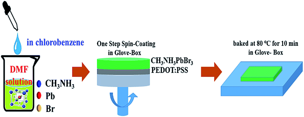
The preparation of the mixed MAPbBr3 perovskites film is summarized in Scheme 1. The PEDOT:PSS was spin-coated onto the quartz substrate (4500 rpm, 40 s) and baked at 120 °C for 20 min under ambient conditions. The MAPbBr3 solution was prepared by dissolving CH3NH3Br and PbBr2 (Xi'an Polymer Light Technology Corp, CH3NH3Br >99.9%, PbBr2 >99.9%) with 1.5![[thin space (1/6-em)]](https://www.rsc.org/images/entities/char_2009.gif) :1 molar ratio in DMF (Alfa-Aesar, anhydrous) solution (the concentration ratio is based on our previous research work11). Then chlorobenzene solution was added dropwise into MAPbBr3 DMF until saturation, in order to accelerate crystallization of perovskites. The precursor solution was spin-coated onto PEDOT:PSS film in the glove-box (H2O and O2 ≤0.1 ppm) at a speed of 4000 rpm for 60 s, and annealed at 80 °C for 10 min.
:1 molar ratio in DMF (Alfa-Aesar, anhydrous) solution (the concentration ratio is based on our previous research work11). Then chlorobenzene solution was added dropwise into MAPbBr3 DMF until saturation, in order to accelerate crystallization of perovskites. The precursor solution was spin-coated onto PEDOT:PSS film in the glove-box (H2O and O2 ≤0.1 ppm) at a speed of 4000 rpm for 60 s, and annealed at 80 °C for 10 min.
 | ||
| Scheme 1 The preparation of the mixed MAPbBr3 perovskites. | ||
X-ray diffraction (XRD) pattern displayed in Fig. 1a gave diffraction peaks at 14.90°, 21.08°, 29.98°, 33.62°, 36.92°, 42.94° and 45.68°, which were assigned to the (100), (110), (200), (210), (211), (220) and (300) planes of perovskites structure, respectively. According to the previous report,30 the XRD indicated pure perovskites phase for MAPbBr3, which suggested a lamellar structure with PbBr2 2D-layer parallel to the substrate. The inset of Fig. 1a showed the MAPbBr3 film (deposited on quartz/PEDOT:PSS substrate) with ∼365 nm UV-light irradiation. The cross-section SEM image of the device has also been given in Fig. 1b, the thicknesses of the MAPbBr3 film was ∼500 nm under the fabrication method. Top view of SEM images of the MAPbBr3 film can be seen in Fig. 1c. It exhibited a uniform and dense surface morphology with average grain size of 300–500 nm. Au NPs used here of 20 nm-diameter size (TEM image in inset Fig. 2a) were synthesized according to the classical Frens method,31 the typical extinction 520 nm of the Au NPs aqueous solution was shown in Fig. 2a. The PL spectra (with ∼365 nm excitation) and absorbance spectra of MAPbBr3 film were shown in Fig. 2a. It can be seen that the MAPbBr3 film showed a typical green emission around ∼534 nm with narrow FWHM of ∼24 nm.
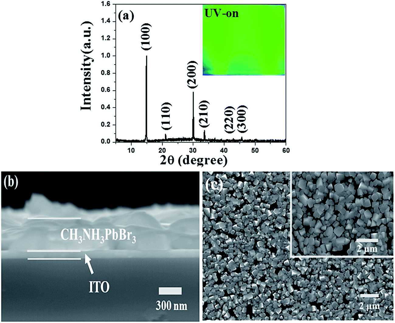 | ||
| Fig. 1 (a) XRD spectra of green-emitting MAPbBr3 crystal film, inset: image of MAPbBr3 film under UV-365 nm excitation, (b) cross-section SEM and (c) SEM image of MAPbBr3 film. | ||
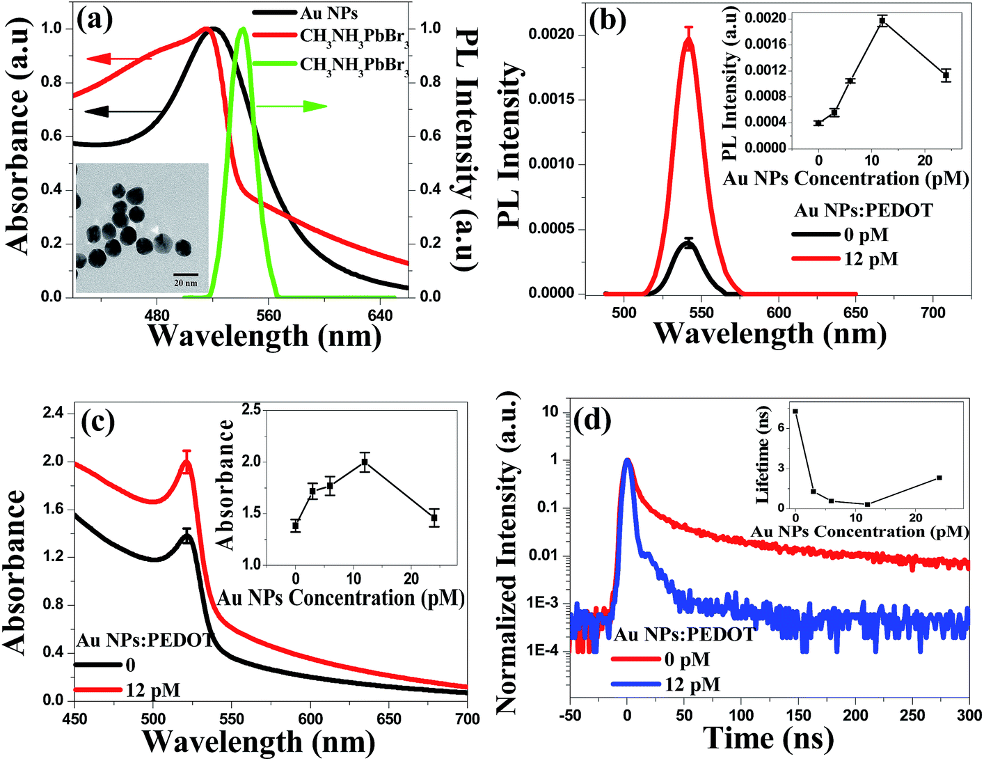 | ||
| Fig. 2 (a) Photoluminescence spectra of MAPbBr3 film, absorbance spectra of MAPbBr3 film and Au NPs aqueous solution respectively, inset: TEM image of Au NPs. (b) Photoluminescence spectra, (c) UV-vis spectra, (d) time-resolved PL spectra in the presence of MAPbBr3 film on PEDOT:PSS doping into Au NPs. The inset in (b–d) is the photoluminescence, UV-vis and time-resolved PL spectra changing uptrend under different Au NPs doping ratio. | ||
The maximum fluorescence intensity enhancement showed about ∼4.0 fold after doping Au NPs into PEDOT:PSS under the optimized concentration 12 pM in Fig. 2b. With the increased Au NPs concentration, the PL intensity increased (in inset Fig. 2b). The absorbance spectra and time-resolved PL spectra in Fig. 2c and d provided the direct evidence of the increased PL intensity. The absorbance intensity of MAPbBr3 film improved 45% under 12 pM concentration Au NPs doping, because of the enhanced absorbance probability (get rid of the Au NPs absorbance).32 The time-resolved PL spectra of MAPbBr3 layer on PEDOT:PSS film in Fig. 2d showed the exciton lifetime is 7.28 ns without Au NPs, but surprisingly, decreases to 0.31 ns with Au NPs. Therefore, time-resolved PL measurement provided the direct observation of the enhanced spontaneous emission rate of MAPbBr3 induced by Au NPs. From the inset in Fig. 2b–d, PL would be decreased until the critical point 12 pM, which maybe due to the nanoparticles aggregation at the high Au NPs density.14,16 High aggregation Au NPs would exposed out of the PEDOT:PSS surface (top view and cross-section of SEM as shown in Fig. 3a–d), then the direct contact between Au NPs and MAPbBr3 film would seriously quench the fluorescence by non-radiative Fröster energy transfer.14,33
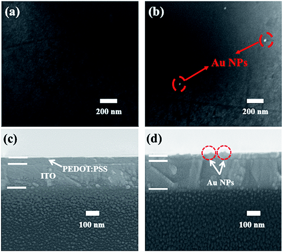 | ||
| Fig. 3 Top view and cross-section of SEM image of the dispersion of Au NPs in PEDOT:PSS under (a) low, (c) none, (b and d) high concentration doping ratio. | ||
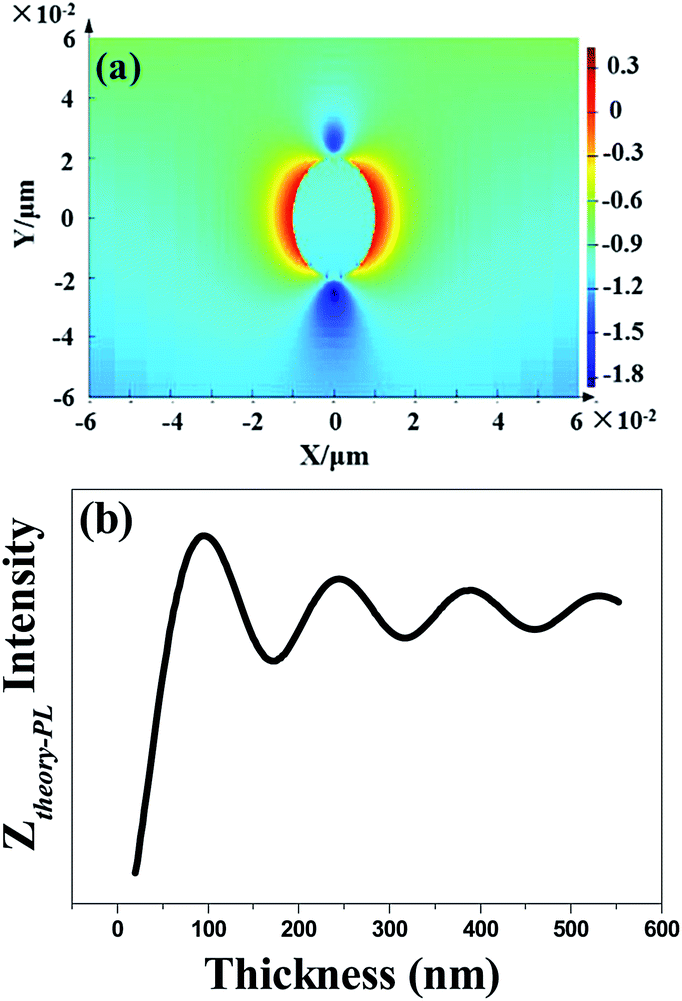
In order to explore the enhancement mechanism, we simulate the near- and far-field model around Au NPs in Fig. 4. The energy matching and distance dependence characters would be the primary difference. For near-field, when the frequency of incident light is located in the resonant frequency of metallic NPs, resonance will occur to form the near-field effect around metallic NPs in the range of 5–10 nm. Fig. 4a shows the near electric-field distribution of 20 nm-Au NPs simulated by finite-different time-domain (FDTD). We can see that the electric-field intensity strongly distribute around the neighbourhood of the NPs, and working distance is in the range of 5–10 nm. The intensity of near-field degraded very quickly as a function of distance, which is nearly disappeared when distance larger than 10 nm. The thickness of PEDOT:PSS thin film is the key factors to determine the effective coupling between near-field and emissive layer. Thus, the thickness of PEDOT:PSS buffer layer (less than 30 nm) would be thin enough to put the emitting layer into the scoped of near-field as shown in Scheme 2a.
 | ||
| Fig. 4 Theoretical simulation of (a) near-electric field profile, (b) far-field distribution. | ||
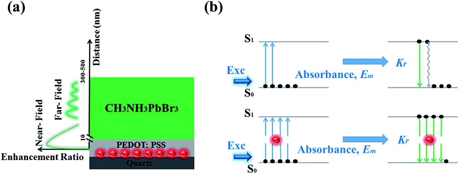 | ||
| Scheme 2 (a) The near- and far-field distribution in devices, (b) diagrams of the procedure of emission without and with Au NPs. | ||
For far-field, the enhancement ratio for respective wavelength is not related to the intrinsic frequency of metallic NPs as in near-field effect, but depends on fluorophore/metallic NPs distance d and refractive index of media n. Thus enhancement for different wavelength would be easily achieved by distance d optimization. We also established the model of far-field enhancement of Au NPs. Recently we demonstrated utilizing far-field of Au NPs to enhance chromophores emissive in the full-visible spectral range in organic light-emitting diodes.14,15,25 The enhancement factor Ztheory-PL of far-field effect is given by
To further deeply understand the mechanism of the effective emissive enhancement by doping Au NPs, we proposed that multiple plasmonic enhancing processes induced by dual-optical effect as shown in Scheme 2b. As shown in Scheme 2b, there are two main processes occur when excited: absorbance and radiative velocity. Firstly in the absorption process, the ground state electrons transit from the lowest vibrational level of S0 to a higher vibrational level of excited state S1 and soon return to the lowest vibrational level of S1 by non-radiative internal conversion (IC) process. Then the excited electrons transit from the lowest vibrational level of S1 to S0 by radiative and non-radiative ways. 20 nm-Au NPs were buried in the PEDOT:PSS film randomly with proper distances to the MAPbBr3 layer. Through multiple surface plasmonic effects, the absorbance probability of MAPbBr3 can be significantly enhanced, therefore more electrons transit to higher energy level S1 by electromagnetic field (combining with Fig. 2c). From the lowest vibrational level of S1 to S0, the addition of Au NPs induces faster radiative velocity (combining with Fig. 2d) and leads enhanced emission. Thus, the presence of Au NPs increases the population excited electrons, and enhance the radiative velocity. Based on the multiple enhancements of absorbance and emission during light excitation, the enhancement of fluorescence will be much more effective under near- and far-field together.
In a conclusion, we achieved about ∼4.0 fold fluorescence enhancement through doping Au NPs into the PEDOT:PSS. Both the experimental and theoretical results have testified that it mainly attributes to multiple near- and far-field effect of Au NPs. The scope of the near- and far-field of Au NPs could both cover with the MAPbBr3 film, which means it in favour of fluorescence enhancement most. And it is also the advantage that utilizing Au NPs enhancing the MAPbBr3 film fluorescence emissive. Our results may offer that Au NPs constitute a feasible and effective rout for achieving high-performance perovskites light-emitting diodes and lasing devices.
Acknowledgements
This work was supported by the National Natural Science Foundation of China (Grant No. 11602243, 11504300, 51473052), NSFA of China (Grant No. U1630125), Natural Science Foundation Project of CQ CSTC (Grant No. cstc2015jcyjA50002).References
- S. D. Stranks and H. J. Snaith, Nat. Nanotechnol., 2015, 10, 391 CrossRef CAS PubMed.
- L. K. Ono, S. H. Wang, Y. Kato, S. R. Raga and Y. B. Qi, Energy Environ. Sci., 2014, 7, 3989 CAS.
- S. A. Velduis, P. P. Boix, N. Yantara, M. Li, T. C. Sum, N. Mathews and S. G. Mhaisalkar, Adv. Mater., 2016, 28, 6804 CrossRef PubMed.
- G. Xing, N. Mathews, S. S. Lim, N. Yantara, X. Liu, D. Sabba, M. Grätzel, S. Mhaisalkar and T. C. Sum, Nat. Mater., 2014, 13, 479 CrossRef PubMed.
- Z. K. Tan, R. S. Moghaddam, M. L. Lai, P. Docampo, R. Higler, F. Deschler, M. Price, A. Sadhanala, L. M. Pazos, D. Credgington, F. Hanusch, T. Bein, H. J. Snaith and R. H. Friend, Nat. Nanotechnol., 2014, 9, 687 CrossRef CAS PubMed.
- X. F. Du, G. Wu, J. Cheng, H. Dang, K. Z. Ma, Y. W. Zhang, P. F. Tang and S. Chen, RSC Adv., 2017, 7, 10391 RSC.
- C. Zhang, K. Wang, N. Yi, Y. Gao, M. Zhu, W. Sun, S. Liu, K. Xu, S. Xiao and Q. Song, Adv. Opt. Mater., 2016, 4, 2057 CrossRef CAS.
- R. Dhanker, A. N. Brigeman, A. V. Larsen, R. J. Stewart, J. B. Asbury and N. C. Giehink, Appl. Phys. Lett., 2014, 105, 151112 CrossRef.
- X. L. Yang, G. J. Zhou and W. Y. Wong, J. Mater. Chem. C, 2014, 2, 1760 RSC.
- Q. Liao, K. Hu, H. H. Zhang, X. D. Wang, J. N. Yao and H. B. Fu, Adv. Mater., 2015, 27, 3405 CrossRef CAS PubMed.
- P. Chen, Z. Y. Xiong, X. Y. Wu, M. Shao, X. J. Ma, Z. H. Xiong and C. H. Gao, J. Phys. Chem. Lett., 2017, 8, 1810 CrossRef CAS PubMed.
- F. Deschler, M. Price, S. Pathak, L. E. Klintberg, D. D. Jarausch, R. Higler, S. Hüttner, T. Leijtens, S. D. Stranks, H. J. Snaith, M. Atatüre, R. T. Phillips and R. H. Friend, J. Phys. Chem. Lett., 2014, 5, 1421 CrossRef CAS PubMed.
- J. H. Peng, X. J. Xu, Y. Tian, J. S. Wang, F. Tang and L. D. Li, Appl. Phys. Lett., 2014, 105, 173301 CrossRef.
- X. Y. Wu, L. L. Liu, W. C. H. Choy, T. C. Yu, P. Cai, Y. J. Gu, Z. Q. Xie, Y. N. Zhang, L. Y. Du, Y. Q. Mo, S. P. Xu and Y. G. Ma, ACS Appl. Mater. Interfaces, 2014, 6, 11001 CAS.
- X. Y. Wu, L. L. Liu, Z. C. Deng, L. Nian, W. Z. Zhang, D. H. Hu, Z. Q. Xie, Y. Q. Mo and Y. G. Ma, Part. Part. Syst. Charact., 2015, 32, 686 CrossRef CAS.
- X. Y. Wu, L. L. Liu, T. C. Yu, L. Yu, Z. Q. Xie, Y. Q. Mo, S. P. Xu and Y. G. Ma, J. Mater. Chem. C, 2013, 1, 7020 RSC.
- Y. H. Su, Y. F. Ke, S. L. Cai and Q. Y. Yao, Light: Sci. Appl., 2012, 1, e14 CrossRef.
- J. H. Peng, F. Tang, X. J. Xu, M. P. Jia and L. D. Li, RSC Adv., 2016, 6, 38148 RSC.
- N. Y. Kim, S. H. Hong, J. W. Kang, N. S. Myoung, S. Y. Yim, S. Jung, K. Lee, C. W. Tu and S. J. Park, RSC Adv., 2015, 5, 19624 RSC.
- J. H. Park, Y. T. Lim, O. O. Park, J. K. Kim, J. W. Yu and Y. C. Kim, Chem. Mater., 2004, 16, 688 CrossRef CAS.
- P. J. Jesuraj and K. Jeganathan, RSC Adv., 2015, 5, 684 RSC.
- W. Y. Ji, J. Wang, Q. H. Zeng, Z. S. Su and Z. C. Sun, RSC Adv., 2013, 3, 14616 RSC.
- M. Gu, X. P. Li and Y. Y. Cao, Light: Sci. Appl., 2014, 3, e177 CrossRef CAS.
- X. Y. Wu, L. L. Liu, Z. Q. Xie and Y. G. Ma, Chem. J. Chin. Univ., 2016, 37, 409 CAS.
- X. Y. Wu, Y. Q. Zhuang, Z. T. Feng, X. H. Zhou, Y. Z. Yang, L. L. Liu, Z. Q. Xie, X. D. Chen and Y. G. Ma, Nano Res., 2017 DOI:10.1007/s12274-017-1614-3.
- J. Kummerlen, A. Leitner, H. Brunner, F. R. Aussenegg and A. Wokaun, Mol. Phys., 1993, 80, 1031 CrossRef.
- C. D. Geddes and J. R. Lakowicz, J. Fluoresc., 2002, 12, 121 CrossRef.
- S. K. Balakrishnan and P. V. Kamat, ACS Energy Lett., 2017, 2, 88 CrossRef CAS.
- X. Zhang, B. Xu, W. Wang, S. Liu, Y. Zheng, S. Chen, K. Wang and X. W. Sun, ACS Appl. Mater. Interfaces, 2017, 9, 4926 CAS.
- B. Yang, X. Mao, S. Q. Yang, Y. J. Li, Y. Q. Wang, M. S. Wang, W. Q. Deng and K. L. Han, ACS Appl. Mater. Interfaces, 2016, 8, 19587 CAS.
- G. Frens, Nat. Phys. Sci., 1973, 241, 20 CrossRef CAS.
- X. H. Zhou, L. L. Liu, X. Y. Wu, Y. Z. Yang, X. F. Jiang, X. D. Chen, Q. H. Xu, Z. Q. Xie and Y. G. Ma, J. Mater. Chem. C, 2017, 5, 1356 RSC.
- S. A. Choulis, M. K. Mathai and V. E. Choong, Appl. Phys. Lett., 2006, 88, 213503 CrossRef.
| This journal is © The Royal Society of Chemistry 2017 |