
 Open Access Article
 This Open Access Article is licensed under a Creative Commons Attribution-Non Commercial 3.0 Unported Licence
The dependence of silver nanowire stability on network composition and processing parameters
Geoffrey Deignanab and
Irene A. Goldthorpe *ab
*ab
aDepartment of Electrical and Computer Engineering, University of Waterloo, Waterloo, ON N2L 3G1, Canada. E-mail: igoldthorpe@uwaterloo.ca
bWaterloo Institute for Nanotechnology, University of Waterloo, Waterloo, ON N2L 3G1, Canada
First published on 17th July 2017
Abstract
Silver nanowires are a promising replacement material for indium tin oxide in transparent electrodes. These nanowires, however, degrade in air due to corrosion and morphological instability. In this work, the composition of silver nanowire networks and common processing parameters used in electrode fabrication are tested for their effect on nanowire stability and electrode lifetime. Smaller diameter nanowires, sparser nanowire networks, higher electrode annealing temperatures and the use of a substrate plasma treatment are all factors which accelerate electrode degradation. The mechanisms of degradation are studied and suggestions to optimize silver nanowire electrode lifetimes are given.
Introduction
Recent interest in silver nanowires (AgNWs) has proliferated due to their ability to replace incumbent transparent conductive oxides, most commonly indium tin oxide (ITO), in electronic devices. Devices such as touch panels, light emitting diodes (LEDs), e-paper, organic light emitting diodes (OLEDs), liquid crystal displays (LCDs), and solar cells all require a thin film with highly transparent and conductive properties to act as a transparent electrode.1 ITO is widely used as a transparent electrode material because of its high conductivity and controllable properties via its deposition method.2,3 However, the high cost of ITO deposition, indium scarcity, and film brittleness are prompting the search for replacement materials.1,2 AgNWs have been materials of interest specifically for the replacement of ITO films since Xia et al. first demonstrated their simple and inexpensive synthesis via the polyol method.4 Because of properties such as low sheet resistance, high transparency, mechanical flexibility and ease of deposition, AgNW-based electrodes are being evaluated for use in commercial touchscreen devices,5 and have also been shown to be candidates for solar applications,6–9 OLED displays,11–13 touch panels,14 and smart windows.15 Furthermore, AgNW networks have recently been demonstrated for other applications including antibacterial films,19 wearable electronics,5 transparent heaters,10 sensors,16–18 and medical devices.20 There exist several reviews of AgNW transparent electrodes and their applications.21–23Because AgNWs are becoming more widely used, the longevity of the material must be addressed. Because AgNWs are thinner than 100 nm, as well as have very high surface area to volume ratios due to their shape and small diameter, instability and corrosion are severe problems. AgNWs have been known to become discontinuous when left in atmospheric conditions for less than 6 months24 which leads to electrode failure. Atmospheric corrosion of bulk and thin-films of silver is a relatively known subject, but far less is known about the stability and degradation of silver nanowires. The few studies on this latter topic focus on the environmental conditions nanowires are exposed to. Humidity,25 elevated temperatures,26 light exposure,25 and sustained electrical currents27 have all been found to accelerate AgNW degradation. However, these factors alone cannot explain why silver nanowires and nanowire electrodes prepared by different groups have vastly different lifetimes. Silver nanowires prepared by Mayousse et al.28 were reported to be stable when stored in ambient atmosphere for two and a half years, while AgNWs prepared by Elechiguerra et al.24 and Jiu et al.25 degrade to the point of non-continuity in as little as 30 days under similar conditions. In the context of transparent electrodes, Mayousse's samples showed a minimal sheet resistance increase in 2.5 years, while the electrodes prepared in two other studies, one by Jiu25 and the other by Vaagensmith,29 were non-conductive via open circuit in less than 6 months. Moon also discussed nanowire corrosion, finding that the resistance of electrodes increased approximately 250% over a time period of 2 months.30 In all these works, the AgNWs were similarly synthesized using the polyol method and it is unclear why their rates of degradation differed. Furthermore, although various transparent and conductive passivation layers have been developed to slow AgNW electrode degradation,30–33 they can't fully prevent the increase of electrode resistance over extended periods of time. Therefore it is important to determine why and how the nanowire film itself affects lifetime to be able to improve passivation technologies and employ additional ways to improve longevity. In this work, we study how the electrode composition and common processing parameters used to fabricate these electrodes affect nanowire stability and electrode lifetimes under passive conditions (i.e. without an applied voltage or current). AgNW electrode films were prepared using a variety of different solvents, substrates, nanowire diameters, film densities, and various pre- and post-deposition processing parameters, then exposed to atmospheric conditions for an extended period of time. The results observed reveal valuable information on what variables affect silver nanowire degradation and therefore how to increase the lifetime of silver nanowire materials. Specifically, it was observed that the nanowire diameter, density, post-deposition annealing temperatures and substrate plasma treatments are parameters that significantly affect the longevity of AgNW electrodes.
Experimental
Electrode preparation
Substrates of heat stabilized polyethylene terephthalate (PET) (ST505 Melinex film, DuPont Teijin Films) and quartz glass having dimensions of 5 cm × 5 cm were sonicated in isopropyl alcohol, acetone, and distilled water for 180 seconds in each respective solvent, then blown dry with a nitrogen gun. Purchased silver nanowires (Blue Nano 90 nm nanowires, Novarials A20, Novarials A70, Seashell California hi-flex e-ink, ACS Materials D50, and ACS Materials D70), with average diameters ranging from 20 to 90 nm and average lengths ranging from 10 to 200 μm were tested. Nanowires were shipped and stored in three different solvents: ethanol, isopropyl alcohol and water. The nanowire solutions were diluted to their desired concentration (experiment dependent) and re-dispersed via mechanical agitation. A small volume of nanowire solution was then pipetted at one end of the desired substrate, and a Mayer rod was slowly rolled to spread the nanowires along the length of the substrate.34–36 The coated substrate was set aside for 3 minutes to allow for solvent evaporation, rotated 90°, and then re-coated using a cleaned Mayer rod. This procedure was repeated two more times to create a random nanowire mesh across the substrate surface.Thermal annealing process
Thermal annealing is the most common post-deposition method which assists in lowering the junction resistance of overlapping nanowires, and causes flowing or partial decomposition of the polyvinylpyrrolidone (PVP) layer that exists on the AgNWs after their polyol synthesis.35,37–39 To test the impact of the annealing temperature on the long-term stability of the nanowires, selected electrodes were annealed in low vacuum at a temperature between 80–180 °C for 30 minutes.38 Electrodes were then completed with application of copper tape at either end for resistance measurements.Mechanical pressing
As an alternative to annealing, the remaining electrodes were subject to room temperature mechanical pressure to lower the nanowire junction resistances.40 This method was both used as a comparison to the thermal treatments, and for other samples where different variables (nanowire diameter, density, etc.) were tested to separate their effects from those caused by annealing. A rolling press (MSK-HRP-01, MTI Corporation, Richmond, USA) with a rolling speed of 5 mm s−1 was used. Electrodes were pressed three times, first with the two rollers spaced 70 μm apart, and then a subsequent two times with a roller spacing of 60 μm. After pressing, copper tape was applied to two ends of the electrode.Corona plasma treatment
For some samples, after cleaning the glass or PET substrate via the procedure listed above, a corona plasma treatment was applied via a SoftLithoBox (BlackHole Lab, Paris).41 The tip was held 1 cm above the surface of the substrate to allow for electrical discharge to reach the surface. The tip was passed over the substrate five times to ensure a full treatment of corona plasma. Plasma-treated substrates were immediately coated with nanowires in the method listed above. No pressing or annealing was performed to these electrodes.Electrode storage conditions
All fabricated electrodes were stored in an atmospherically regulated environment (average temperature 24 ± 1 °C, humidity 40 ± 2%) with ambient airflow for 60 days. The electrodes were stored in the dark to avoid any photonic influences on nanowire behaviour throughout the test. Electrodes were periodically removed for several seconds every 3 days throughout the study for sheet resistance measurements.Characterization
Electrode sheet resistances were measured with 2 probes via a multimeter. Their specular transparencies were recorded with a spectrophotometer, subtracting out the contribution of the substrate. Scanning electron microscope (SEM) micrographs were taken with a LEO 1550 GEMINI system. Non-conductive samples were coated with 10 nm of gold to prevent surface charging effects. Energy dispersive X-ray spectroscopy (EDS) was performed in the SEM to determine the chemical composition of larger features. For the latter case, NW films were deposited on conductive silicon wafer substrates to avoid the need for gold coating. Bright-field transmission electron microscope (TEM) images and EDS spectra of smaller features were acquired with a JEOL 2010F TEM.Results and discussion
Degradation artifacts
Before presenting how the various electrode and processing parameters affect nanowire degradation, we first compile the main degradation artifacts that were observed since they are common to several parameters. After 60 days in atmosphere, silver nanowires degrade and become discontinuous in more than one manner. Fig. 1 shows the morphology and chemical composition of the three main degradation artifacts that were observed. First, shown in Fig. 1a, is the formation of many small nanoparticles along the surface of a nanowire. TEM-EDS spectra of these nanoparticles (which, because of the spatial resolution of the technique, also includes some of the NW body as well) show that other than carbon originating from the TEM grid and silicon signal from the detector, only silver and sulfur are present. From studies on bulk silver it is well known that silver does not form a native oxide in atmospheric conditions, but rather silver sulfide (Ag2S) is the dominant product of corrosion.42–45 The latter occurs via the reaction of surface silver with atmospheric hydrogen sulfide (H2S) and carbonyl sulfide (OCS), even though these have very low ambient concentrations of 5 ppb and 0.5 ppb, respectively.45 Ag2S nucleates at random locations on the surface of silver and tends not form a uniform film.43 Morphologies including dendrites, clumps and whiskers have been observed on bulk and thin films of silver. For AgNWs, we along with several other reports observe that Ag2S exists as particles along the surface of the nanowire body.24,25,27,28 After the 60 day experiment some silver nanowires corroded to the point of discontinuity, as displayed in Fig. 1a.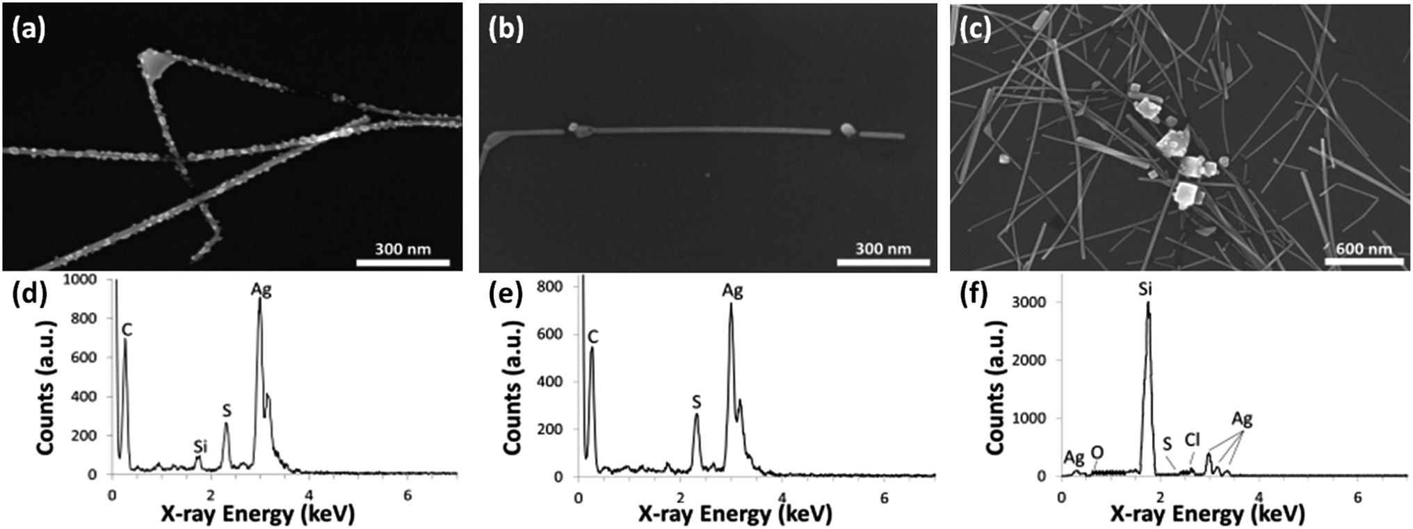 | ||
| Fig. 1 SEM images of silver nanowires exposed to atmosphere for 60 days. There are 3 main types of degradation artifacts observed: (a) small Ag2S particles on the surface of nanowires, (b) spherical silver particles intercepting a nanowire, and (c) clusters of larger agglomerations of silver. (d) TEM-EDS spectrum of one nanoparticle on the surface of a nanowire in ‘a’ and its immediate surroundings, (e) TEM-EDS spectrum one particle intercepting the nanowire in ‘b’, and (f) SEM-EDS of a larger particle in ‘c’ (the silicon peak originates from the substrate). | ||
Corrosion of AgNWs was present under all experimental parameters tested in this work, but was not always the dominant failure mechanism causing discontinuity in the nanowire network. Spherical particles intercepting the nanowire body were observed as a second artifact causing discontinuity of nanowires over the 60 days (Fig. 1b). This artifact was observed in thinner diameter nanowires either in sparser networks or ones isolated from the main AgNW network. Nanowires with these intercepting particles do not have small Ag2S nanoparticles on their surfaces. High-resolution TEM shows that the intercepting particles are polycrystalline, and EDS analysis of several of the particles indicates that they are predominantly silver (85–91%), with 1–2% chlorine and 7–13% sulfur. Regarding the chlorine, this atomic percentage is slightly higher than in areas of the nanowire away from the particles (<1%). AgCl can be a result of Ag reacting with trace amounts of Cl2 and HCl in the ambient.44,45,61 The chlorine could also be left over from the synthesis process as NaCl is commonly used in the polyol synthesis method. Regardless, the majority of the particles are Ag suggesting that they do not primarily exist of corrosion products, but are rather a result of a rearrangement of silver from the nanowire into nanoparticle form due to the morphological instability of the nanowire. These issues will be discussed in the sections below.
The last major artifact observed was clusters of larger agglomerations that were prevalent in dense networks of thinner nanowires. From the SEM image in Fig. 1c, one can see that there is no presence of either Ag2S nanoparticle growth or intercepting spherical particles in any of the nanowires in the vicinity of the agglomerations. SEM-EDS results show that the large agglomerations consisted primarily of Ag (90–94%) with some amount of Cl (6–10%) and trace sulfur (silicon is present in the EDS spectrum due to its use as a substrate material). Thus, the large particles are mostly silver that has likely diffused from the AgNWs in the network.46,47 This will be discussed further below. The diffusion of silver atoms causes discontinuities in nanowires in the network, as can be seen in Fig. 1c.
Effect of parameters on sheet resistance
Nanowire diameter, nanowire concentration, annealing temperature, and substrate plasma treatment were all variables that had a significant effect on the resistance change of the nanowire network over time. Fig. 2 shows the effect of these variables on electrode sheet resistance over a period of 60 days of ambient atmospheric exposure. Other variables tested had little effect on sheet resistance. Neither the type of solvent used to disperse the nanowires in solution (ethanol, water, isopropyl alcohol), nor the age of the nanowires in solvent before deposition (i.e. time spent on shelf) affected the rate of degradation. The substrate used (glass vs. PET) and the average length of the nanowires also had no effect.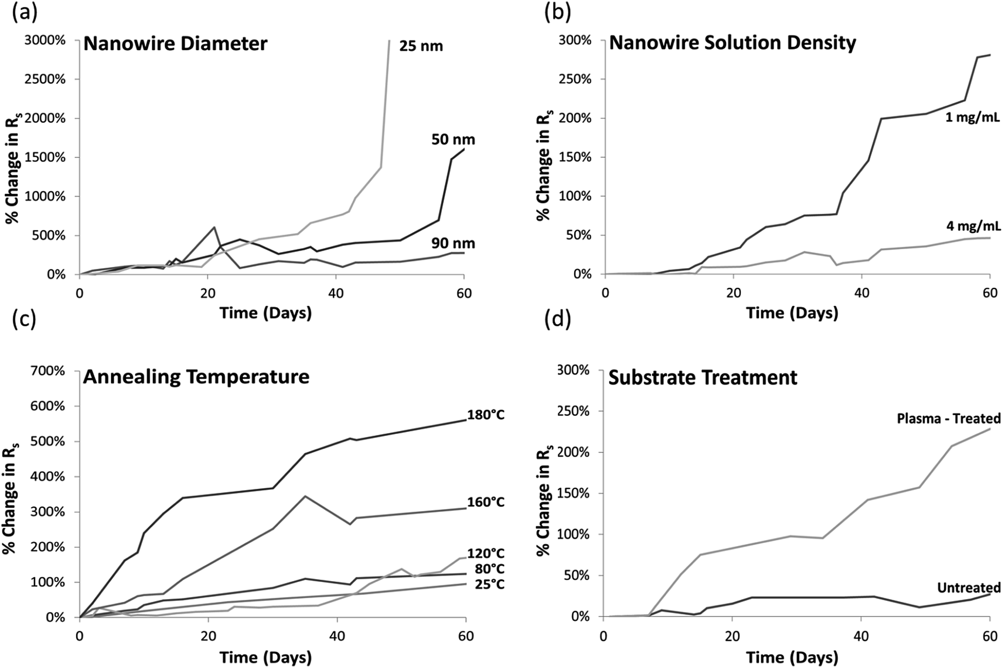 | ||
| Fig. 2 The effect of electrode and processing parameters on electrode sheet resistance (Rs) when left in air for 60 days. (a) Nanowire diameter, (b) nanowire density, (c) annealing temperature, (d) substrate plasma treatment. | ||
In the subsections below the effect of the significant variables – diameter, density, annealing temperature, and plasma treatment – are discussed in more detail.
Effects of diameter
Fig. 2a plots the resistance of electrodes prepared with different diameter nanowires deposited with the same nanowire solution concentration of 4 mg mL−1. Electrodes consisting of thinner nanowires degraded significantly faster than those with thicker nanowires. After 60 days, the sheet resistance of electrodes with 90 nm and 50 nm diameter nanowires increased 250% and 1600%, respectively. Electrodes with 25 nm diameter nanowires reached an open-circuit before the 60 days was over.The degradation of larger diameter nanowires (greater than 40 nm in diameter) is primarily caused by corrosion creating Ag2S nanoparticles on their surface, as shown in Fig. 1a and again in Fig. 3a. The thicker the nanowire, the longer it takes for corrosion to advance to the point where the nanowire becomes discontinuous. Therefore, electrodes made from thicker nanowires have longer lifetimes.
 | ||
| Fig. 3 Images of silver nanowires left in atmosphere for 60 days. (a) TEM image of larger diameter (90 nm) nanowires indicating corrosion. (b) SEM image of smaller diameter (20 nm) nanowires showing particles at the location of disconnects in the nanowires. TEM images showing the progression of particle formation in small diameter nanowires over time: (c) beginning of bottleneck formation, (d) a bottleneck which has progressed into discontinuity, (e) a spherical particle and a wider nanowire disconnection. | ||
In smaller diameter nanowires (diameters less than 40 nm), degradation by the corrosion depicted in Fig. 1a was scarcely observed. Rather, as seen in Fig. 3b, the prevalent degradation matches the artifact depicted in Fig. 1b. Fig. 3c–e displays TEM images of smaller diameter nanowires at different stages of degradation, from bottlenecking (Fig. 3c), to disconnection (Fig. 3d), to particle formation (Fig. 3e). The morphological changes in the nanowire, coupled with the EDS data showing that the main composition of the spherical particles is silver rather than corrosion products (Fig. 1e), indicate that nanowire instability rather than corrosion is the primary reason for thin nanowire degradation. The surface-area-to-volume ratio of nanowires scales with 1/r, where r is the radius of the nanowire. Thus this ratio is more than 3.5 times higher for a cylindrical 25 nm diameter nanowire versus a 90 nm nanowire. And because surfaces have higher energy than atoms in bulk, thinner nanowires are less stable than thicker ones. This is particularly true for Ag nanowires whose side facets are {100},48 which for face-centre-cubic materials have higher energy than the lowest energy {111} facets. Furthermore, silver nanowires synthesized from the polyol process have strain energy caused by a combined 7.35° gap between the triangular prisms forming the pentagonal wire.49 The observation of thin metal nanowires breaking into smaller segments has been observed and studied by others and is often attributed to Rayleigh instability.38,50–54
Although corrosion appears to play a smaller role in the degradation of thin nanowires, we found it is likely still a necessary factor. A network of 25 nm diameter nanowires was left for 60 days in a desiccated low vacuum chamber rather than in atmosphere, where there are low levels of sulfur and chlorine containing gases, as well as low humidity. When in this low vacuum environment, the sheet resistance increased by only 6% and no discontinuities were observable via SEM. Thus the content of the atmosphere clearly plays a role in the instability of thin nanowires, and could be due to the humidity which is known to increase corrosion rates25 in addition to the existence of corrosion-causing gases.
SEM data show that the instability of thin nanowires in air causes a larger proportion of them being discontinuous after 60 days compared to thicker diameter nanowires. The latter are more stable due to their lower surface area per volume and instead degrade due to corrosion which leads to discontinuities at a much slower rate. These observations explain the more rapid resistance increase of the electrodes containing 25 nm diameter nanowires in Fig. 2a compared to electrodes with 50 and 90 nm diameter nanowires.
Effects of density
As seen in Fig. 2b, the sheet resistance of dense nanowire networks (made with a solution concentration of 4 mg mL−1) increased only 50%, while a sparse network (solution concentration = 0.2 mg mL−1) containing nanowires of the same diameter and prepared in the same manner, increased by over 300%.The varying density electrodes were prepared with 20 nm diameter nanowires. Since the diameter was small, little evidence of the type of corrosion depicted in Fig. 1a is observed, as discussed in the section above. However, microscopy imaging did reveal the degradation features in the dense and sparse networks differed. In sparse networks (solution concentration ≤0.5 mg mL−1), the formation of small particles as described in Fig. 1b is dominant. However, in dense networks (solution concentration ≥4 mg mL−1) the dominant degradation feature is instead the one depicted in Fig. 1c. Originally it was thought that the large particulate formations in the latter were artifacts of AgNW synthesis that penetrated the filtration mechanisms used for nanowire purification, but SEM of freshly synthesized networks had no evidence of such large particles. Only after exposure to ambient conditions were these features first observed.
The EDS analysis of such features (Fig. 1f) indicates that these agglomerations are composed primarily of elemental Ag, like the small particles encountered in sparse networks. The volume of silver in these particles is larger than amount of the silver missing from the nanowires in their immediate vicinity. It appears that much of the Ag in the particles have diffused from nanowires further away, as evidenced by gaps in nanowires up to 1.5 μm away from the agglomerations. The gaps do not have small particles intercepting them and it is hypothesized this is because the small particles that result from nanowire instability, or the silver that would otherwise lead to them, diffuse and coalesce to form the larger agglomerations similar to an Oswald ripening process. Because the surface-to-volume ratio of particles decreases with their size, a large particle is more energetically favourable than multiple smaller particles. Larger particles are not observed in sparser networks likely because the small particles are far apart and they would need to diffuse markedly longer distances to coalesce.
Although the appearance of degradation differed among sparse and dense networks, it was found from extensive SEM imaging that the proportion of nanowires with an electrical discontinuity was the same for all densities tested. Regardless of the network density, there was one discontinuity per 1 μm length of nanowire on average after 60 days of exposure to ambient conditions. Thus, a denser network did not increase nanowire stability. Rather, dense networks have a slower increase in resistance because if a nanowire becomes discontinuous, there exists other pathways through which the current can flow. Sparser networks, on the other hand, have fewer alternative conductive pathways when an electrical disconnection occurs.
Effect of annealing temperature
When AgNW films are deposited on a substrate without further processing, locations where nanowires overlap have a high resistance which can lead to film sheet resistances in the MΩ □−1 range. Annealing significantly lowers junction resistances and therefore film sheet resistance by welding the overlapping nanowires, and is the most commonly used and convenient method to do so. 200 °C for 30 minutes is a common procedure for 90 nm diameter silver nanowires.35,37–39 The effect of the annealing temperature on electrode lifetimes, however, has not previously been studied. Although a 30 minute anneal significantly reduces the initial sheet resistance, it accelerates the rate of degradation over the long term. Fig. 2c, where 25 nm diameter AgNWs are annealed at different temperatures, reveals that the higher the annealing temperature used, the faster the electrode resistance increases over time. The sheet resistance of electrodes annealed at 180 °C for 30 min increased 590% over the 60 day time period compared to 137% for samples annealed at 80 °C. The resistance of electrodes that were mechanically pressed at room temperature rather than annealed rose 97%.Two samples of 90 nm diameter nanowires, one annealed at 150 °C for 30 min and one pressed at room temperature after nanowire film deposition, were imaged every 2 weeks for 60 days. Immediately after annealing, AgNWs processed at both temperatures visually looked similar under the SEM except for a waviness induced in the pressed nanowires due to the mechanical pressure. However, TEM imaging revealed that while the unannealed AgNWs had a 1–3 nm thick layer of PVP on their surfaces, this layer did not exist in the annealed sample. Fig. 4 compares the morphology of unannealed and annealed samples after two weeks of exposure to ambient conditions. There are only the beginnings of corrosion particle formation (particles <10 nm in diameter) in the unannealed nanowires, whereas the annealed nanowires had larger (40–50 nm in diameter) and more numerous Ag2S particles. This level of degradation observable in the annealed sample is parallel to the level of degradation observable in unannealed samples after 6 weeks of exposure to ambient. This trend continued, with the unannealed nanowires undergoing the same corrosion mechanisms as the annealed nanowires but at a much slower rate, explaining the slower rise in sheet resistance over time observed in Fig. 2c.
 | ||
| Fig. 4 SEM images of silver nanowires after 2 weeks of exposure to ambient conditions. Nanowires were (a) pressed at room temperature and (b) annealed at 150 °C for 30 min after deposition. Notice the lager corrosion particles on the surface of the annealed nanowires. | ||
It was expected that annealing would accelerate degradation during the 30 minutes process, since both nanowire corrosion and instability are worsened at elevated temperatures.45,50 However, it was somewhat surprising that the 30 minute anneal accelerated degradation over the entire 60 day period, as evidenced by the higher slopes of the curves in Fig. 2c compared to the room temperature processed electrode. This may be due to increased silver atom diffusion at higher temperatures, and defects formed during the anneal would increase reactivity with sulfur afterwards, in turn leading to faster formation of Ag2S. Small notches or bottlenecks in the nanowire, like in Fig. 3c, may also be initiated during the anneal, and once these are formed further evolution into disconnections may be accelerated.
Another factor may be due to the reduction or removal of the PVP layer from the nanowire surface during anneals above ∼150 °C (the exact temperature depends on the molecular weight of PVP used during nanowire synthesis).55 With less PVP, H2S and OCS gases may be able to reach and adsorb on the silver surface more easily and thus more corrosion would occur. This hypothesis echoes that of Elechiguerra et al. who hypothesized that a thicker layer of PVP on AgNWs would improve overall stability.24 This hypothesis may also explain why the rate of degradation (related to the slope of the curves in Fig. 2c) is higher for annealing temperatures above 150 °C compared to annealing temperatures of 80 °C and 120 °C, as the latter two conditions would not be high enough to significantly reduce the PVP layer.
Due to the lower rate of degradation, mechanically pressing a nanowire film at room temperature is an attractive alternative to annealing. At a transparency of 88% (wavelength = 550 nm), nanowires pressed on PET substrates have a sheet resistance of 23 Ω □−1. This is similar to annealed electrodes on glass and far superior to annealed electrodes on PET. The latter is because PET cannot tolerate temperatures above 100 °C due to permanent deformation. Nanowire electrodes annealed on PET at 100 °C have an average sheet resistance of approximately 300 Ω □−1 at 87% transparency (wavelength = 550 nm).
Effect of plasma treated substrates
Plasma treatments increase the hydrophilicity of a substrate surface to aid in the adhesion of a subsequently deposited material without the need for chemical modification. They are commonly used for the preparation of AgNW electrodes to increase the adhesion of the nanowires to glass or plastic substrates.30,56,57 Fig. 2d shows, however, that a corona plasma treatment significantly affects the rate of NW electrode degradation. After 60 days, the sheet resistance of the treated substrate was 4× that of an untreated substrate. It is hypothesized this is because of the increased hydrophilicity of the substrate which would attract more moisture. This surface water provides a medium for the absorption of corrosion-causing gases as well the dissolution of silver ions and therefore increases corrosion rates.50 It is well known that AgNWs degrade faster in humid environments.47Conclusions
Our results show that common variations in the composition and processing of silver nanowire electrodes, namely nanowire diameter, nanowire density, annealing temperature, and substrate plasma treatment, significantly affect the rate of electrode degradation. This explains some of the large variation of sheet resistance increases from one report to the next. Regarding the nanowire electrodes mentioned in the introduction, Mayousse's electrodes, which were the ones with long lifetimes, were annealed at a low temperature of 80 °C compared to 140 °C for both Moon and Vaagensmith.29,30 Jiu instead used high intensity pulsed light to sinter the AgNW networks which causes silver to eject electrons via the photoelectric effect, resulting in a faster rate of corrosion due to the formation of Ag+ ions.25,58 The Mayousse electrodes were also quite dense. Through image processing of images provided in their papers, the Mayousse nanowire density was 27 mg m−2 compared to 5 and 17 mg m−2, respectively, used by Vaagensmith and Jiu. All 5 studies mentioned in the introduction used different nanowire diameters. And lastly, Moon and Vaagensmith used a plasma treatment whereas the other researchers did not. These factors are all in addition to environmental differences between the various studies which are known to have significant effects on corrosion rates.In addition to explaining varying degradation rates, this study also gives guidance on how to design electrodes with longer lifetimes. According to our results, electrodes consisting of dense networks of larger diameter nanowires that are processed at room temperature and are not exposed to corona plasma should fare better than other electrodes. Regarding the latter two variables, mechanical pressing is an alternative option to both annealing and corona plasma treatment, since pressing both welds nanowire junctions as well as increases nanowire adhesion to plastic substrates.40,59 Regarding dense and thick nanowires, this may not always be possible due to design considerations. Denser nanowire films result in lower transparencies, and larger diameter nanowires lead to more haze which is undesirable for certain applications such as display technologies. If nanowire diameters less than 40 nm are used, our study suggests that in addition to passivation layers which block corrosion-causing gases, strategies to increase their morphological stability may be helpful such as low temperature hydrogen gas processing60 or passivating the silver surfaces with dielectric layers.61,62
Regardless of the electrode composition and processing conditions, our results show that some degradation will still occur and an effective passivation strategy will still be necessary. For many applications, the passivation layer needs to be both transparent and conductive, block gas, be mechanically flexible, and cost effective. Although many passivation materials have been studied, more work needs to be done before AgNW electrodes can be used as a viable ITO replacement in a range of applications. Furthermore, as this study only deals with the passive stability of AgNWs, other phenomena must be taken into account when dealing with AgNWs in real devices under electrical bias.
Conflict of interest
The authors declare that they have no competing interests.Author's contributions
GD participated in the study design, carried out the experiments, and drafted the manuscript for submission. IAG supervised the project, participated in the design of the study and results analysis, and revised the manuscript. Both authors approved the final manuscript for publication.Abbreviations
| AgNW | Silver nanowire |
| ITO | Indium tin oxide |
| LED | Light emitting diode |
| OLED | Organic light emitting diode |
| LCD | Liquid crystal display |
| PET | Polyethylene terephthalate |
| PVP | Polyvinylpyrrolidone |
| SEM | Scanning electron microscope |
| TEM | Transmission electron microscope |
| EDS | Energy dispersive X-ray spectroscopy |
Acknowledgements
This work was supported by the Natural Science and Engineering Research Council (NSERC) of Canada.References
- D. Langley, G. Giusti, C. Mayousse, C. Celle, D. Bellet and J.-P. Simonato, Nanotechnology, 2013, 24, 1–20 CrossRef PubMed.
- A. Kumar and C. Zhou, ACS Nano, 2010, 4, 11–14 CrossRef CAS PubMed.
- P. Edwards, A. Porch, M. Jones, D. Morgan and R. Perks, Dalton Trans., 2004, 19, 2995–3002 RSC.
- Y. Sun, B. Gates, B. Mayers and Y. Xia, Nano Lett., 2002, 2, 165–168 CrossRef CAS.
- G.-W. Huang, H.-M. Xiao and S.-Y. Fu, Sci. Rep., 2015, 5, 13971 CrossRef PubMed.
- L. Yang, T. Zhang, H. Zhou, S. C. Price, B. J. Wiley and W. You, ACS Appl. Mater. Interfaces, 2011, 3, 4075–4084 CAS.
- H.-S. Kim, M. Patel, H.-H. Park, A. Ray, C. Jeong and J. Kim, ACS Appl. Mater. Interfaces, 2016, 8, 8662–8669 CAS.
- J.-Y. Lee, S. T. Connor, Y. Cui and P. Peumans, Nano Lett., 2010, 10, 1276–1279 CrossRef CAS PubMed.
- W. Gaynor, J.-Y. Lee and P. Peumans, ACS Nano, 2010, 4, 30–34 CrossRef CAS PubMed.
- T. Kim, Y. W. Kim, H. S. Lee, H. Kim, W. S. Yang and K. S. Suh, Adv. Funct. Mater., 2013, 23, 1250–1255 CrossRef CAS.
- X.-Y. Zeng, Q.-K. Zhang, R.-M. Yu and C.-Z. Lu, Adv. Mater., 2010, 22, 4484–4488 CrossRef CAS PubMed.
- Z. Yu, Q. Zhang, L. Li, Q. Chen, X. Niu, J. Liu and Q. Pei, Adv. Mater., 2011, 23, 664–668 CrossRef CAS PubMed.
- L. Li, Z. Yu, W. Hu, C.-H. Chang, Q. Chen and Q. Pei, Adv. Mater., 2011, 23, 5563–5567 CrossRef CAS PubMed.
- W. Hu, X. Niu, R. Zhao and Q. Pei, Appl. Phys. Lett., 2013, 102, 083303 CrossRef.
- H. H. Khaligh, K. Liew, Y. Han, N. M. Abukhdeir and I. A. Goldthorpe, Sol. Energy Mater. Sol. Cells, 2015, 132, 337–341 CrossRef.
- M. Amjadi, A. Pichitpajongkit, S. Lee, S. Ryu and I. Park, ACS Nano, 2014, 8, 5154–5163 CrossRef CAS PubMed.
- J. Wang, J. Jiu, M. Nogi, T. Sugahara, N. Shijo, H. Koga, P. He and K. Suganuma, Nanoscale, 2015, 7, 2926–2932 RSC.
- L. Xu, Y. Hou, M. Zhang, T. Cheng, W. Huang, C. Yao and Q. Wu, Anal. Methods, 2015, 5649, 7 Search PubMed.
- Y. Chen, W. Lan, J. Wang, R. Zhu, Z. Yang, D. Ding, G. Tang, K. Wang, Q. Su and E. Xie, Physica E, 2016, 76, 88–94 CrossRef.
- N. Leavitt, ClearOhm Silver Nanowires in Breakthrough Medical Application, Cambrios Adv. Mater., Sunnyvale, CA, 2015 Search PubMed.
- T. Sannicolo, M. Lagrange, A. Cabos and C. Celle, Small, 2016, 44, 6052–6075 CrossRef PubMed.
- F. Basarir, F. Irani, A. Kosemen, B. Camic, F. Oytun, B. Tunaboylu, H. Shin, K. Nam and H. Choi, Mater. Today, 2017, 3, 60–72 CrossRef.
- D. Langley, G. Giusti, C. Mayousse, C. Celle, D. Bellet and J. Simonato, Nanotechnology, 2013, 24, 452001 CrossRef PubMed.
- J. L. Elechiguerra, L. Larios-Lopez, C. Liu, D. Garcia-Gutierrez, A. Camacho-Bragado and M. J. Yacaman, Chem. Mater., 2005, 17, 6042–6052 CrossRef CAS.
- J. Jiu, J. Wang, T. Sugahara, S. Nagao, M. Nogi, H. Koga, K. Suganuma, M. Hara, E. Nakazawa and H. Uchida, RSC Adv., 2015, 5, 27657–27664 RSC.
- M. Lagrange, T. Sannicolo, D. Munoz-Rojas, B. Guillo Lohan, A. Khan, M. Anikin, C. Jiménez, F. Bruckert, Y. Bréchet and D. Bellet, Nanotechnology, 2017, 28, 055709 CrossRef CAS PubMed.
- H. H. Khaligh and I. A. Goldthorpe, Nanoscale Res. Lett., 2013, 8, 235 CrossRef PubMed.
- C. Mayousse, C. Celle, A. Fraczkiewicz and J.-P. Simonato, Nanoscale, 2015, 7, 2107–2115 RSC.
- B. Vaagensmith and Q. Qiao, IEEE J. Photovolt., 2016, 6, 1549–1553 CrossRef.
- I. K. Moon, J. I. Kim, H. Lee, K. Hur, W. C. Kim and H. Lee, Sci. Rep., 2012, 3, 1112 CrossRef.
- Y. Ahn, Y. Jeong and Y. Lee, ACS Appl. Mater. Interfaces, 2012, 4, 6410–6414 CAS.
- K. Jaito, N. Yoshinaga, E. Tsutsumi and Y. Akasaka, Synth. Fibre Mater., 2013, 175, 42–46 CrossRef.
- A. Kim, H. Lee, H.-C. Kwon, H. S. Jung, N.-G. Park, S. Jeong and J. Moon, Nanoscale, 2016, 8, 6308 RSC.
- A. A. Tracton, Wire-Wound Rod Coating, Coatings Technology; Fundamentals, Testing, Processing Techniques, Francis Group, Boca Raton, Taylor, 2006, pp. 19-1–19-7 Search PubMed.
- L. Hu, H. S. Kim, J.-Y. Lee, P. Peumans and Y. Cui, ACS Nano, 2010, 4, 2955–2963 CrossRef CAS PubMed.
- C.-H. Liu and X. Yu, Nanoscale Res. Lett., 2011, 6, 75 CrossRef PubMed.
- J.-Y. Lee, S. T. Connor, Y. Cui and P. Peumans, Nano Lett., 2008, 8, 689–692 CrossRef CAS PubMed.
- D. P. Langley, M. Lagrange, C. Jiménez, G. Giusti, Y. Bréchet, N. Nguyen and D. Bellet, Nanoscale, 2014, 6, 135355 RSC.
- S. B. Sepulveda-Mora and S. G. Cloutier, J. Nanomater., 2012, 2012, 7 Search PubMed.
- H. H. Khaligh and I. A. Goldthorpe, Nanoscale Res. Lett., 2014, 9, 310 CrossRef PubMed.
- A. Schutze, J. Y. Jeong, S. E. Babayan, J. Park, G. S. Selwyn and R. F. Hicks, IEEE Trans. Plasma Sci., 1998, 26, 1685–1694 CrossRef CAS.
- D. W. Rice, P. Peterson, E. B. Rigby, P. B. P. Phipps, R. J. Cappell and R. Tremoureux, J. Electrochem. Soc., 1981, 128, 275–284 CrossRef CAS.
- H. Bennett, R. Peck, D. Burge and J. Bennett, J. Appl. Phys., 1969, 40, 3351 CrossRef CAS.
- A. Czanderna, J. Phys. Chem., 1964, 68, 2765–2771 CrossRef CAS.
- J. Franey, G. Kammlott and T. Graedel, Corros. Sci., 1985, 25, 133–143 CrossRef CAS.
- R. Hoffmann and D. Turnbull, J. Appl. Phys., 1951, 22, 634–639 CrossRef.
- C. Tomizuka and E. Sonder, Phys. Rev., 1956, 103, 1182–1184 CrossRef CAS.
- E. Marzbanrad, G. Rivers, P. Peng, B. Zhao and N. Y. Zhou, Phys. Chem. Chem. Phys., 2015, 17, 315–324 RSC.
- W. A. Saidi, H. Feng and K. A. Fichthorn, J. Phys. Chem., 2012, 117, 1163–1171 Search PubMed.
- S. Karim, M. Toimil-Molares, A. Balogh, W. Ensinger, T. Cornelius, E. Khan and R. Neumann, Nanotechnology, 2006, 17, 5954–5959 CrossRef CAS.
- E. C. Garnett, W. Cai, J. J. Cha, F. Mahmood, S. T. Connor, M. G. Christoforo, Y. Cui, M. D. McGehee and M. L. Brongersma, Nat. Mater., 2012, 11, 241–249 CrossRef CAS PubMed.
- A. Volk, D. Knez, P. Thaler, A. W. Hauser, W. Grogger, F. Hofer and W. E. Ernst, Phys. Chem. Chem. Phys., 2015, 17, 24570–24575 RSC.
- S. Karim, M. Toimil-Molares, W. Ensinger, A. Balogh, T. Cornelius, E. Khan and R. Neumann, J. Phys. D: Appl. Phys., 2007, 40, 3767 CrossRef CAS.
- H. Oh, J. Lee, J.-H. Kim, J.-W. Park and M. Lee, J. Phys. Chem., 2016, 120, 20471–20477 CAS.
- X. M. Zeng, G. P. Martin and C. Marriott, Int. J. Pharm., 2001, 218, 63–73 CrossRef CAS PubMed.
- K. Gotoh, A. Yasukawa and Y. Kobayashi, Polym. J., 2011, 43, 545–551 CrossRef CAS.
- A. Popelka, I. Krupa, I. Novak, M. A. S. A. Al-Maadeed and M. Ouederni, J. Phys. D: Appl. Phys., 2016, 50, 035204 CrossRef.
- H. M. Yates, L. A. Brook and D. W. Sheel, Int. J. Photoenergy, 2008, 2008, 870392 CrossRef.
- T. Tokuno, M. Nogi, M. Karakawa, J. Jiu, T. T. Nge, Y. Aso and K. Suganuma, Nano Res., 2011, 4, 1215–1222 CrossRef CAS.
- M. Losurdo, I. Bergmair, M. M. Giangregorio, B. Dastmalchi, G. V. Bianco, C. Helgert, E. Pshenay-Severin, M. Falkner, T. Pertsch, E.-B. Kley, U. Huebner, M. A. Verschuuren, M. Muehlberger, K. Hingerl and G. Bruno, J. Phys. Chem., 2012, 116, 23004–23012 CAS.
- S. D. Standridge, G. C. Schatz and J. T. Hupp, J. Am. Chem. Soc., 2009, 131, 8407–8409 CrossRef CAS PubMed.
- D. Chanda, K. Shigeta, S. Gupta, T. Cain, A. Carlson, A. Mihi, A. J. Baca, G. R. Bogart, P. Braun and J. A. Rogers, Nat. Nanotechnol., 2011, 6, 402–407 CrossRef CAS PubMed.
| This journal is © The Royal Society of Chemistry 2017 |