
 Open Access Article
 This Open Access Article is licensed under a Creative Commons Attribution-Non Commercial 3.0 Unported Licence
A low-power consumption MZI thermal optical switch with a graphene-assisted heating layer and air trench
Yue Sun,
Yue Cao,
Yunji Yi *,
Liang Tian,
Yao Zheng,
Jie Zheng,
Fei Wang and
Daming Zhang
*,
Liang Tian,
Yao Zheng,
Jie Zheng,
Fei Wang and
Daming Zhang
State Key Laboratory on Integrated Optoelectronics, College of Electronic Science & Engineering, Jilin University, Changchun 130012, P. R. China. E-mail: yiyj@jlu.edu.cn
First published on 16th August 2017
Abstract
To reduce the power consumption of thermal optical switches, graphene-assisted hybrid MZI structures were designed and simulated. The hybrid waveguide structures were composed of polymer cores, silica lower claddings, air trenches, and graphene-assisted heating layers. Because of the high thermal-optic coefficient of the polymer, excellent thermal conductivities of silica and graphene, and the air trench structures, the power consumption of the hybrid structures could be reduced to below 0.95 mW. The graphene-assisted heating layers were also designed to bury the waveguide cores or to contact the surface of the waveguide cores for more efficiently conducting the heat of electrodes to the waveguide cores. Moreover, the side heating electrodes introduced were found to be compatible with the designed graphene-assisted heating layers. The polarization and the absorption of both rectangle and ridge waveguide structures were analyzed through optical field simulation. Based on the optimized parameters, the thermal fields were simulated, and the heating efficiencies of the graphene-assisted hybrid structures could be increased by 78% as compared to those of the top electrode device without a graphene layer. Our simulation comprises two MZI thermal optical switches with an optimized balance between the switching power consumption and the switching time. One MZI thermal optical switch with a lower power consumption realized the switching power consumptions of only 0.39 mW and the switching times of 30 μs and 92.4 μs, whereas the other switch with faster switching times achieved the switching power consumptions of 0.95 mW and the switching times as fast as 1 μs and 81.6 μs.
Introduction
Thermal-tuning optical devices include tunable filters, variable optical attenuators, and thermal optical switch. Thermal optical switch is a fundamental element in optical communication networks for realizing switching function through the thermo-optic effect. The present research on a thermo-optic switch focuses on reducing the power consumption and improving the response speed from the aspects of material and structure.From the aspects of material, polymer and inorganic material are two fundamental materials used in thermal optical switches.1–3 Polymer thermal optical switches have the advantage of low-power consumptions because of high thermal optical coefficient of the polymer. However, inorganic material thermal optical switches have a faster switching time. To achieve a balance between power consumption and switching time, hybrid integration with the polymer core and inorganic cladding has been massively investigated. In 2014, Liang Lei fabricated the organic/inorganic hybrid MZI thermo-optic switch with a switching power of 7.2 mW and response time of 100 μs.4 In 2014, Xie Nan fabricated low-power, high-speed polymer buried channel waveguide thermo-optic switches with a switching power of 3.5 mW and a response time of 200 μs.5 The abovementioned hybrid devices take the materials into account, but the structures of cladding and substrate have not been optimized.
From the aspects of structure, addition of air trenches to thermal optical switches is an effective way to reduce the power consumption. With a cladding air trench, the thermal field was mainly restricted in the waveguide region. In 2008, a novel 2 × 2 thermo-optic MMI switch was designed, where only one heat electrode was used with air and silicon trenches, and the applied power was 1.35 mW.6 In 2015, a thermal optical switch with an air trench (switching time of 150 μs and the power consumption of 3.4 mW) has been reported.7 With a substrate air trench, the mutual interference of the tuning branch and untuning branch could be eliminated. Even for the trench structure, a large portion of the heating power was wasted by the waveguide cladding. The function of the cladding was to reduce the optical loss caused by the metal electrode absorption. Thus, the electrode absorption would be a main restriction for the further reduction of the power consumption. A low optical absorption electrode material fabricated beside or in contact with the optical waveguide core would be a feasible solution to this problem.
Graphene, as a revolutionary two-dimensional (2D) sheet material with extraordinary mechanical, electronic, and photonic properties, has attracted significant attention in many fields. In the field of optics, graphene has been integrated with a waveguide device used for the polarizer,8 detector,9 modulator,10,11 and optical switch.12 For the thermal optical switches, the integration of graphene and polymer will also lead to a revolutionary promotion of the switching properties. In 2014, non-local heating for thermally tuning nano-photonic has been achieved using a graphene heat conductor, and the 90% rising and decaying times are simulated to be 9 μs.13 In 2015, graphene has been introduced as a transparent nanoheater of the thermally photonic microdisk resonators, and the rising time and decaying time are measured to be 12.8 μs and 8.8 μs, respectively.14 Graphene-based waveguide thermal-optic switch is an effective way to increase the heating efficiency. Graphene has been used as a heat conductor or heating electrode of silicon waveguide due to its feature of splendid thermal conductivity and electro-conductivity.15,16
In this study, we have demonstrated a graphene-based hybrid waveguide thermal optical switch with an air trench. Based on the polymer core, inorganic lower cladding, and air trench, a graphene-assisted heating layer was designed to bury or contact the polymer waveguide core. Moreover, two waveguide structures and two graphene locations were designed. In addition, the polarization, absorption, heating efficiency, and switching properties were simulated and optimized.
Simulation and design
Device structure
The device structure was composed of a polymer waveguide core, metal electrode, and graphene-assisted heating layer. The metal electrode was located beside the waveguide,17 and the graphene-assisted heating layer was contacted or buried in the waveguide core, as was shown in Fig. 1.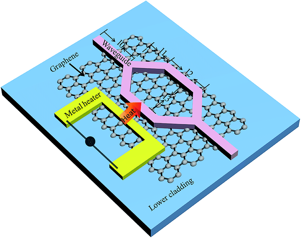 | ||
| Fig. 1 The structure of the thermal optical switch with a graphene-assisted heating layer. | ||
The position of graphene determines the optical loss and the thermal filed distribution. Based on the position of graphene (in the centre or at the bottom) and the waveguide type (rectangular or ridge structure), four basic structures were simulated, as shown in Fig. 2. The corresponding parameters are indicated in the figure, and the dimension parameters of the waveguide are w (width), h (height), h1 (ridge height), and d (separation width between the waveguide and the side metal heating electrode). SU-8 (refractive index: 1.575@1550 nm) was selected as the polymer waveguide core material due to its lithography and photobleaching fabrication methods, which were compatible with the waveguide structure and graphene transfer method. Due to different material features, silicon was selected as the substrate and heat sink with the thickness of 5 μm. As the lower cladding material, silica (refractive index: 1.450) was compared with the PMMA (refractive index: 1.490) material. Air and PMMA have been selected as the upper cladding, and the refractive index is 1 and 1.490, respectively. The heater material is gold, and its refractive index is 0.559 + 11.5i. The refractive index of graphene is 2.973 + 2.79i.18
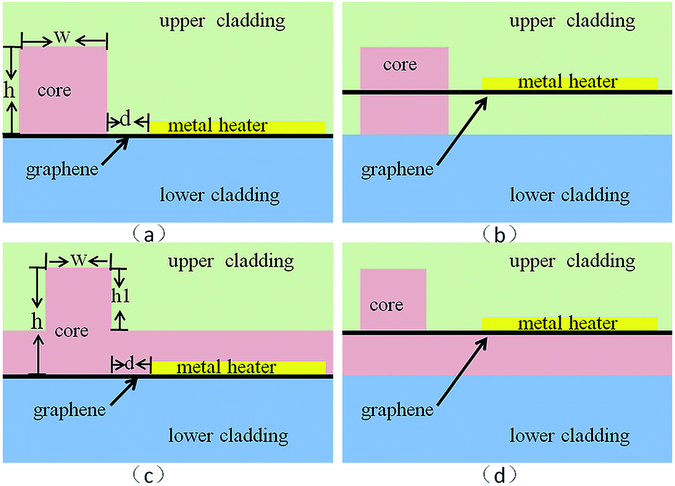 | ||
| Fig. 2 The four structures of a thermal optical switch with a graphene-assisted heating layer: (a) bottom heating rectangular structure, (b) centre heating rectangular structure, (c) bottom heating ridge structure, and (d) centre heating ridge structure. | ||
Optical field
To ensure the single-mode condition, the rectangle waveguide dimension was selected to be 2 μm × 2 μm, and the ridge waveguide width (w), ridge height (h1), and waveguide height (h) were selected to be 3 μm, 3 μm, and 5 μm, respectively. The integrated graphene layer would bring polarization absorption to the waveguide, and the absorption of TE and TM mode caused by the graphene layer was simulated.19,20 Fig. 3 shows the effective optical field distribution of the TE and TM mode. When the graphene layer was at the bottom of the core, the effective optical field of the TE-pass polarizer was simulated, as shown in (a) and (c). Moreover, the effective optical field of the TM-pass polarizer was simulated, as shown in (b) and (d), with the graphene layer at the centre of the core. The optical absorption of the 1 cm graphene conductive layer of the TE and TM mode is calculated to be 94.36 dB and 13.86 dB of the bottom heater rectangular waveguide structure, respectively. For the centre heater rectangular waveguide structure, the optical absorption of the TE and TM mode is calculated to be 480.84 dB and 10.5 dB, respectively. For the bottom heater ridge waveguide structure, the optical absorption for the TE and TM mode is calculated to be 28.68 dB and 4.24 dB, respectively. The optical absorption of the TE and TM mode is calculated to be 244.74 dB and 6.59 dB for the center heater ridge waveguide structure, respectively. The equation is as follows:| Absorption = 10LkNneff = 10L2π/λNneff | (1) |
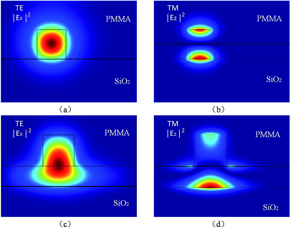 | ||
| Fig. 3 The effective optical field for graphene absorption. (a) The effective optical field of the TE mode in the rectangle waveguide. (b) The effective optical field of the TM mode in the rectangle waveguide. (c) The effective optical field of the TE mode in the ridge waveguide. (d) The effective optical field of the TM mode in the ridge waveguide. | ||
Due to the absorption of the electrode, the distance between the waveguide and the electrode should be optimized to ensure a high heating efficiency and low optical loss. The absorption of rectangular and ridge waveguide with the changing distance between the waveguide and the electrode is shown in Fig. 4. For the rectangular waveguide structure, when the electrodes were located at the bottom of the core, the electrode had only a little influence on the optical absorption. Moreover, when the electrode was located at the side of the rectangle waveguide core, the distance between the rectangle waveguide and the electrode was optimized to be larger than 1 μm. In the ridge waveguide structure, the optimized distance between the waveguide and the electrode was 3 μm, as shown in Fig. 4(b).
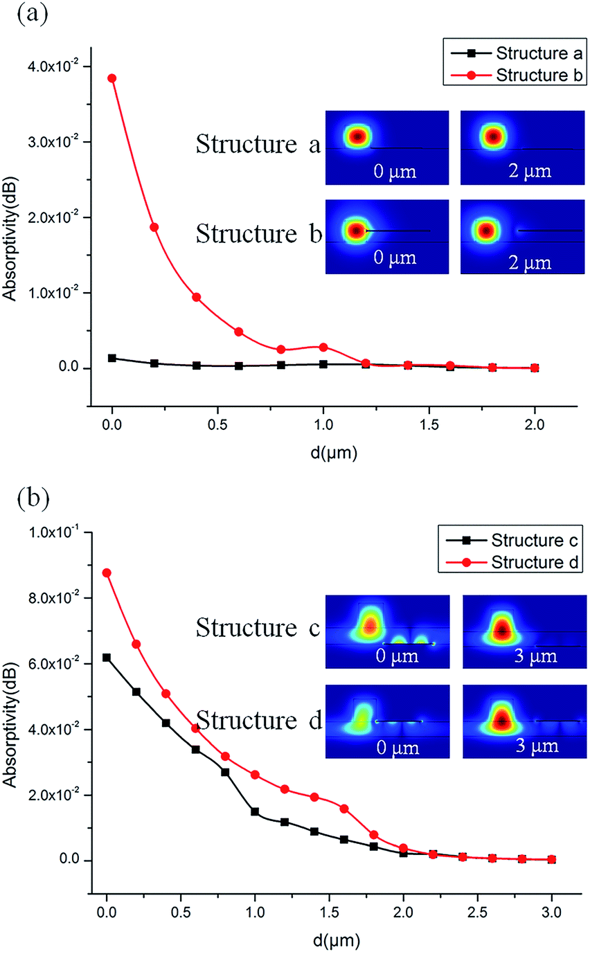 | ||
| Fig. 4 (a) The absorption of the gold electrode of rectangular waveguide structure@1550 nm. (b) The absorption of the gold electrode of ridge waveguide structure@1550 nm. | ||
Thermal field optimization
The thermal field is associated with the heating efficiency of the electrode. When the temperature contrast is fixed, a higher waveguide core temperature means a higher heating efficiency. The relationship between the heating efficiency and the distance between the waveguide core and the electrode was simulated, the simulation parameters are listed below: SU-8 (thermal conductivity: 0.2 W m−1 K−1), silica (thermal conductivity: 0.27 W m−1 K−1), PMMA (thermal conductivity: 0.19 W m−1 K−1), air (thermal conductivity: 0.023 W m−1 K−1), and graphene (thermal conductivity: 5300 W m−1 K−1). The gold heater is 0.1 μm thick and has a width of 6 μm. The external temperature is 295 K. The relation between the temperature of the core centre and the distance between electrode and core is shown in Fig. 5. The part of the steady-state thermal field is shown in the inset of Fig. 5. The effect of distance between the heater and the core layer on the heating efficiency is calculated and compared. | ||
| Fig. 5 The relation between the central temperature of core (T) and the width between waveguide and side electrode (d). | ||
Compared to that of the polymer, the thermal conductivity of air is 1/10 to polymer. The comparison of the thermal field between the structure with polymer upper cladding and the structure with air upper cladding is shown in Fig. 6. In the rectangular structure (Fig. 6(a) and (b)), which had a metal heater next to the core, the central temperature of the waveguide was 297.42 K and 298.36 K, respectively. With air cladding, the thermal field can be concentrated in the waveguide core layer, and the heating efficiency is superior.
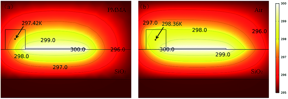 | ||
| Fig. 6 The thermal field (a) polymer upper cladding and (b) air upper cladding. | ||
Compared with that of silica, the thermal conductivity of the polymer is relatively poor. The thermal field of the polymer lower cladding structure was simulated and compared with that of the silica lower cladding structure, as shown in Fig. 7. It can be seen that the influence of the lower cladding material is not obvious. The deep air trench structure has been ameliorated (see Fig. 8(a)), and the temperature of the waveguide core (299.44 K) was greatly improved.
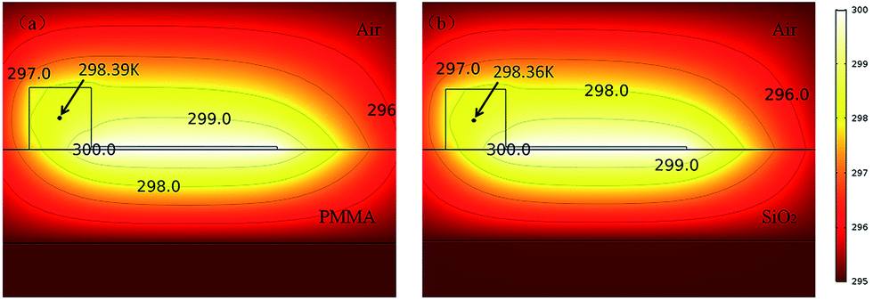 | ||
| Fig. 7 The thermal field (a) polymer lower cladding and (b) inorganic lower cladding. | ||
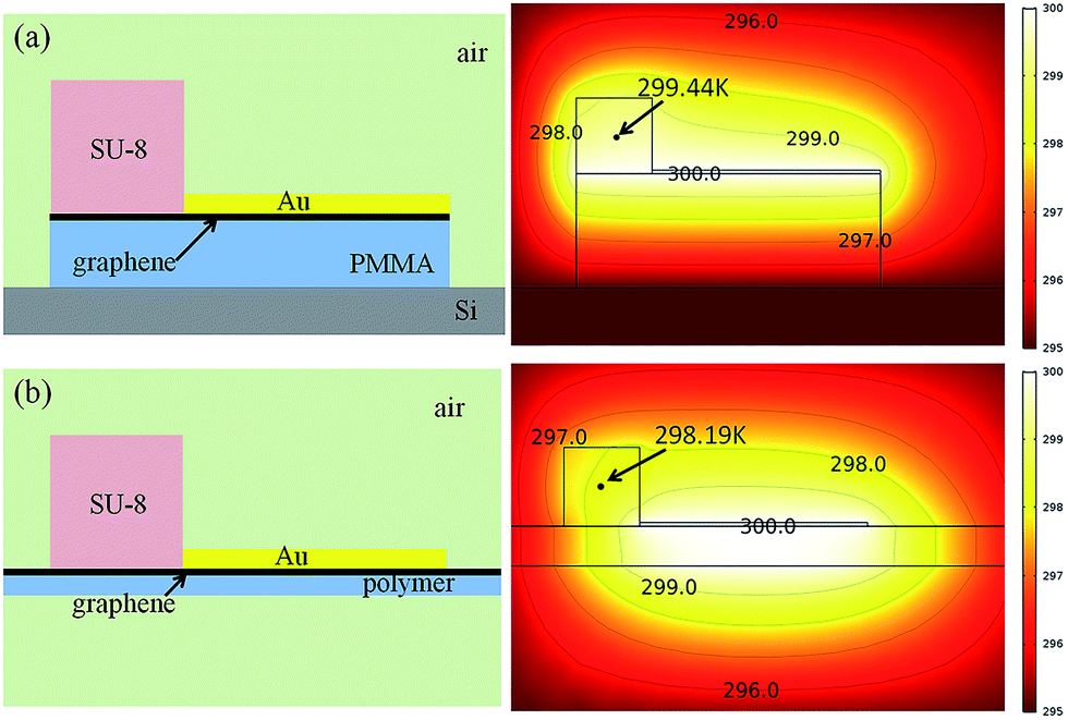 | ||
| Fig. 8 The structure and thermal field (a) ameliorated air trench structure and (b) flexible structure. | ||
One of the unique features of polymer materials is their flexibility. By taking advantage of their flexibility, we designed the structure shown in Fig. 8(b). Moreover, the thin layer of the polymer is doped with a highly thermally conductive material as the lower cladding of the waveguide. The flexible waveguide with a high thermal conductivity can thus be implemented (thermal conductivity: 500 W m−1 K−1).
To balance the optical absorption and the heating efficiency, the optimized parameters of the four structures are shown in Table 1.
| Length (μm) date structure | w | h | h1 | d |
|---|---|---|---|---|
| Bottom heating rectangular structure | 2 | 2 | — | 0 |
| Centre heating rectangular structure | 2 | 2 | — | 1 |
| Bottom heating ridge structure | 3 | 5 | 3 | 3 |
| Centre heating ridge structure | 3 | 5 | 3 | 3 |
To compare the power consumption of the top electrode polymer thermal optical switch and the graphene-assisted ones, the heating electrode length (l2) was selected to be equal to the length of the M-Z branch, which had a length of 1 cm. The distance between the two arms of the M-Z structure was selected to be 30 μm (l3). As is shown in Fig. 9(a), the heating electrode has little influence on the other waveguide. The corresponding parameters of l0 and l1 were 500 μm and 500 μm, respectively. The optical field of the device is shown in Fig. 9(b).
 | ||
| Fig. 9 (a) The thermal field and (b) optical field of the switch when l1 = 500 μm, l2 = 1 cm, and l3 = 30 μm. | ||
According to the interference theory of the thermo-optical switch, the phase shift is associated with the effective index changes caused by the electrode. The change of effective refractive index was simulated with the changing electrode heating temperature. When the phase change is 1/4 cycles, the thermo optic switch has a switching effect. Fig. 10 shows the relation between the phase changes and the temperature changes of the heater (the device structure as shown in Fig. 11, the conventional waveguide with top heater). Herein, 2.1 K is the required temperature. The rise time, fall time, and power consumption were calculated, as shown in the right of Fig. 11.
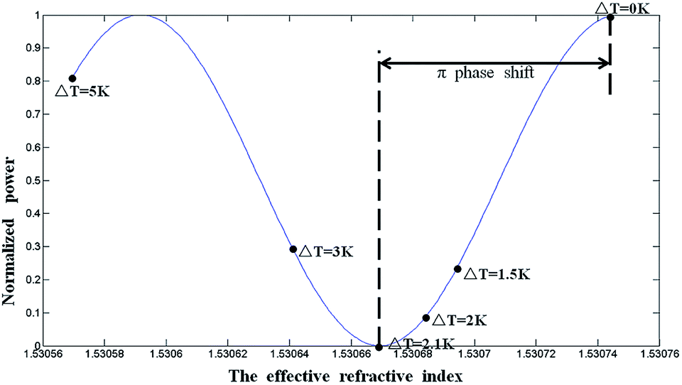 | ||
| Fig. 10 The relation between the phase change and the temperature change of the heater. | ||
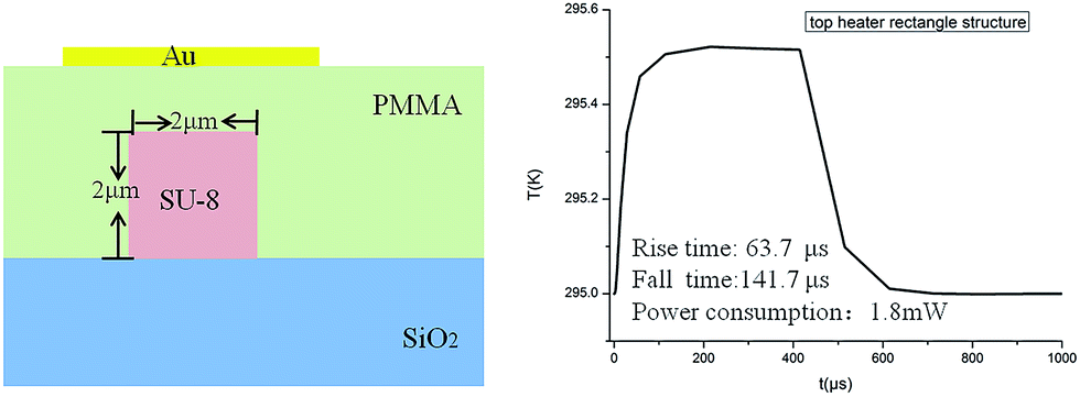 | ||
| Fig. 11 Cross-section of conventional waveguide with top heater and the relationship between temperature and time. | ||
According to the analysis of the light and thermal field of the four kinds of structures, the switching rise time and fall time were calculated (see the Fig. 12).
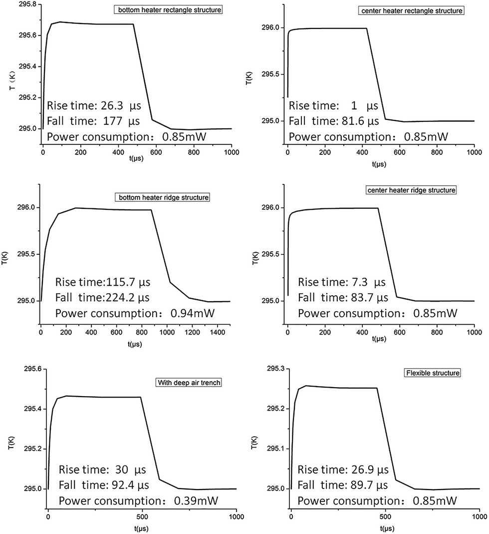 | ||
| Fig. 12 The relationship between temperature and time of different structures and corresponding rise time, fall time, and power consumption. | ||
Conclusions
Hybrid MZI thermal optical switches with a graphene-assisted heating layer and air trench and a power consumption of below 0.95 mW were proposed. Due to the air trench and excellent thermal conductivity of graphene, the heating efficiency can be increased by 45–78% as compared to that of the traditional device. The optimized central heating rectangle structure possess the rise and fall time of 1 μs and 81.6 μs, respectively, with a power consumption of 0.85 mW. The optimized deep air trenching central heating rectangle structure possess the rise and fall time of 30 μs and 92.4 μs, respectively, with the power consumption of 0.39 mW.Acknowledgements
This work was supported by the National Natural Science Foundation of China (NSFC) [61605057, 61475061, 61575076; 61377058], Science and Technology Development Plan of Jilin Province [20140519006JH], and Excellent Youth Foundation of Jilin Province [20170520158JH].Notes and references
- R. L. Espinola, M.-C. Tsai, J. T. Yardley and R. M. Osgood Jr, Fast and low-power thermo optic switch on thin silicon-on-insulator, IEEE Photonics Technol. Lett., 2003, 15(10), 1366–1368 CrossRef.
- L. Liang, C.-T. Zheng, Y.-F. Yan, X.-Q. Sun, F. Wang, C. S. Ma and D.-M. Zhang, Low-power and high-speed thermo-optic switch using hybrid silica/polymer waveguide structure: design, fabrication and measurement, J. Mod. Opt., 2012, 59(12), 1084–1091 CrossRef CAS.
- Y.-F. Liu, X.-B. Wang, J.-W. Sun, J. Sun, F. Wang, C.-M. Chen, X.-Q. Sun, Z.-C. Cui and D.-M. Zhang, Improved performance of thermal-optic switch using polymer/silica hybrid and air trench waveguide structures, Opt. Lett., 2015, 40(9), 1888–1891 CrossRef CAS PubMed.
- L. Liang, L. Qv, L. Zhang, C. Zheng, X. Sun, F. Wang and D. Zhang, Fabrication and characterization on an organic/inorganic 2 × 2 Mach-Zehnder interferometer thermo-optic switch, Photonics and Nanostructures, 2014, 12(2), 173–183 CrossRef.
- X. Nan, H. Takafumi and U. Katsuyuki, Design and Performance of Low-Power, High-Speed, Polarization-Independent and Wideband Polymer Buried Channel Waveguide Thermo-Optic Switches, J. Lightwave Technol., 2014, 32(17), 3067–3073 CrossRef.
- A. M. Al-Hetar, I. Yulianti and A. S. M. Supa'At, et al., Thermo-optic multimode interference switches with air and silicon trenches, Opt. Commun., 2008, 281(18), 4653–4657 CrossRef CAS.
- Y.-F. Liu, X.-B. Wang, J. Sun, H.-J. Gu, X.-Q. Sun, C.-M. Chen, F. Wang and D.-M. Zhang, Thermal field analysis of polymer/silica hybrid waveguide thermo-optic switch, Opt. Commun., 2015, 356, 79–83 CrossRef CAS.
- X. Yin, T. Zhang, L. Chen and X. Li, Ultra-compact TE-pass polarizer with graphene multilayer embedded in a silicon slot waveguide, Opt. Lett., 2015, 40(8), 1733–1736 CrossRef CAS PubMed.
- L. Yu, J. Zheng, Y. Xu, D. Dai and S. He, Local and nonlocal optically induced transparency effects in graphene silicon hybrid nanophotonic integrated circuits, ACS Nano, 2014, 8(11), 11386–11393 CrossRef CAS PubMed.
- S. Gan, C. Cheng, Y. Zhan, B. Huang, X. Gan, S. Li, S. Lin, X. Li, J. Zhao, H. Chen and Q. Bao, A highly efficient thermo-optic microrin modulator assisted by graphene, Nanoscale, 2015, 7, 20249–20255 RSC.
- M. Liu, X. Yin, E. Ulin-Avila, B. Geng, T. Zentgraf, L. Ju, F. Wang and X. Zhang, A graphene-based broadband optical modulator, Nature, 2011, 474, 64–67 CrossRef CAS PubMed.
- X. Gan, C. Zhao, Y. Wang, D. Mao, L. Fang, L. Han and J. Zhao, Graphene-assisted all-fiber phase shifter and switching, Optica, 2015, 2(5), 468–471 CrossRef CAS.
- L. Yu, Y. Yin, Y. Shi, D. Dai and S. He, Thermally tunable silicon photonic microdisk resonator with transparent graphene nanoheaters, Optica, 2016, 3(2), 159–166 CrossRef CAS.
- L. Yu, D. Dai and S. He, Graphene-based transparent flexible heat conductor for thermally tuning nanophotonic integrated devices, Appl. Phys. Lett., 2014, 105, 251104 CrossRef.
- K. S. Novoselov, A. K. Geim, S. V. Morozov, D. Jiang, Y. Zhang, S. V. Dubonos, I. V. Grigorieva and A. A. Firsov, Electric field effect in atomically thin carbon films, Science, 2004, 306(5696), 666 CrossRef CAS PubMed.
- R. Prasher, Graphene spreads the heat, Science, 2010, 328, 185–186 CrossRef CAS PubMed.
- Z. Chang and K. S. Chiang, Experimental verification of optical models of graphene with multimode slab waveguides, Opt. Lett., 2016, 41(9), 2129–2132 CrossRef PubMed.
- Z. Zhang and N. Keil, Thermo-optic devices on polymer platform, Opt. Commun., 2016, 362, 101–114 CrossRef CAS.
- Q. Bao and K. Ping Loh, Graphene photonics, plasmonics, and broadband optoelectronic devices, ACS Nano, 2012, 6(5), 3677–3694 CrossRef CAS PubMed.
- J. W. Weber, V. E. Calado and M. C. M. van de Sanden, Optical constants of graphene measured by spectroscopic ellipsometry, Appl. Phys. Lett., 2010, 97, 091904 CrossRef.
| This journal is © The Royal Society of Chemistry 2017 |