DOI:
10.1039/C7RA06444F
(Paper)
RSC Adv., 2017,
7, 33757-33763
Biomimetic nano/micro double-textured silicon with outstanding antireflective and super-hydrophilic surfaces for high optical performance
Received
8th June 2017
, Accepted 27th June 2017
First published on 5th July 2017
Abstract
We report the fabrication of nano/micro double-textured silicon (NMDT-Si) and its structural, optical, and surface wetting properties. The micro-pyramidal textured (MPTs) are formed on the Si surface by a simple potassium hydroxide-based wet etching process. On the other hand, for pillar-arrayed nano-textures (NTs), the thermally-dewetted gold (Au) nanoparticles are employed on the surface of the MPT-Si as an etch mask and the inductively coupled plasma etching is followed. The optical reflectance of the NMDT-Si is strongly dependent on the period and height of NTs on the surface of the MPT-Si, which can be controlled by the Au film thickness and etching time, respectively. Compared with the planar nano-textured Si, the NMDT-Si shows superior antireflection (or higher light absorption) and light-scattered propagation behaviors, which are verified from a finite-difference time-domain simulation, over wide ranges of wavelengths (350–1100 nm) and incident angles (0–70°), resulting in the average reflectance of ∼2.1% and the solar weighted absorption of ∼98.5% at normal incidence, respectively. In addition, it has a super-hydrophilic surface with water contact angles of <5°.
Introduction
Light management such as light scattering, antireflection, and light trapping has been widely researched for high performance of silicon (Si)-based optical and optoelectronic devices including solar cells, photodetectors, and image sensors.1 For high optical performance, the surface modification of Si with high refractive indices of >3.5 at visible and near-infrared wavelengths is essential to suppress the high natural reflectivity (>30%) with strong spectral dependence for its planar surface. Generally, thin-film stacked antireflection coatings (ARCs) with a quarter-wavelength optical thickness and surface texturing technologies are widely used in industrial production of Si-based optical and optoelectronic devices. However, although the thin-film stacked ARC can reduce the surface reflection below 3–5%, it works only in narrow spectral bandwidth and limited incident angle, including additional drawbacks of stress caused by thermal expansion mismatch, adhesion to substrate, and material selection.2 On the other hand, texturing easily forms micro-scale pyramidal arrays on the Si surface using an acid or alkaline (H2SO4, HNO3:H2O, NaOH, KOH, etc.) wet etching process,3,4 but their average reflectivity is kept above 10% though the micro-textures can lead to the strong light scattering, which is insufficient for high-efficiency Si-based optical and optoelectronic devices, especially, solar cells.5 As one of effective approaches, hierarchical double-scale architectures (i.e., nano- and micro-structures), like ‘moth eye’, create superior antireflection in wide ranges of wavelengths and incident angles as well as self-cleaning ability.6–8 However, the reflection of nano/micro double-textured surfaces is mainly dependent on the shape, period, and height of nano-structures.9 Thus, it is necessary to optimize the period and size of nano-patterns and the etching conditions for efficient antireflection. The nano-structures on micro-pyramidal arrays have been realized using a variety of nano-texturing techniques, such as cesium chloride (CsCl) self-assembly lithography (i.e., nano-islands), metal (e.g., silver, gold, nickel, etc.)-assisted chemical etching (catalyst nanoparticles), mask-free plasma (SF6/O2) surface processing, and nano-porous aluminum etch mask.6,10 Recently, a thermal-dewetting process of metal films as cost-effective and facile lithography has been widely employed to form the nano-patterns (i.e., metallic nano-sized cluster or particles) as a dry-etch mask.11,12 In this nano-patterning, the period and size of metallic nano-patterns are determined by the thickness of metal films.11,13
Meanwhile, the surface wettability is also important in outdoor applications since a super-hydrophobic or super-hydrophilic structure can remove dust particles or any contaminants on its surface by water droplets (i.e., self-cleaning), which can maintain the device efficiency by preventing the degradation of optical performance.14 The super-hydrophobic or super-hydrophilic surface can be obtained by introducing the high roughness into the planar surface.15,16
In this work, we fabricated the nano/micro-structured Si using double-texturing processes. To form the micro-pyramidal textures (MPTs) on the Si surface, the chemical wet etching was carried out using a mixture solution of potassium hydroxide (KOH) and isopropyl alcohol (IPA), forming micro-scale pyramidal arrays, because of its good control and reproducibility. The nano-textures (NTs) were fabricated by the Au film thermal-dewetting and dry etching processes, subsequently. For comparison, the nano-texturization was also treated on the planar Si surface from the same nano-texturing fabrication process. For all the samples, the structural and optical properties were systematically studied by adjusting the Au film thickness and etching time. Angle-dependent reflectance characteristics were explored under s-, p-, and un-polarized lights. To theoretically analyze the optical light-scattering propagation inside Si, we conducted finite-difference time-domain (FDTD) simulations. Moreover, the surface wettability was also investigated.
Experimental and simulation modeling details
Fabrication of the NMDT-Si
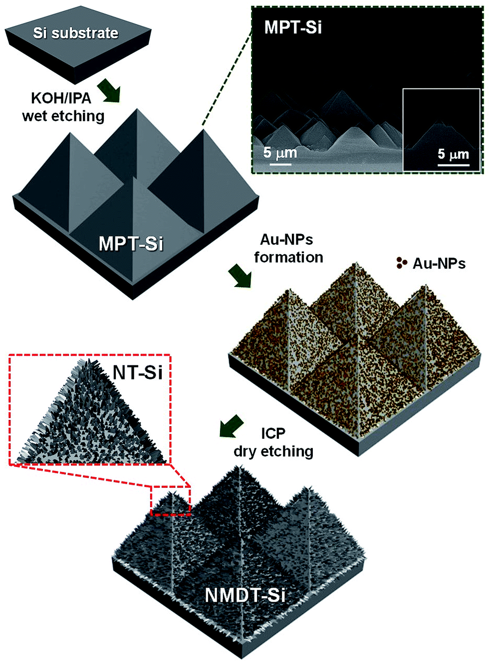
Fig. 1 shows the schematic illustration of process steps for the fabrication of double-textured Si consisting of nano-structures on micro-pyramidal arrays (NMDT-Si) using a combination of wet and dry etching processes. The scanning electron microscope (SEM) image of the micro-pyramidal textured Si (MPT-Si) is also shown in Fig. 1. In this experiment, single-side polished Si substrates with a square area of 2 × 2 cm2 were cleaned with acetone, methanol, and de-ionized water for 10 min, subsequently. And then, we further performed a plasma (ozone) cleaning process to remove the impurities and contaminants on the Si surface for 10 min. To fabricate the MPT-Si, we simply soaked the Si substrates in a mixed solution of KOH![[thin space (1/6-em)]](https://www.rsc.org/images/entities/char_2009.gif) :IPA (10:3 vol%) at a temperature of 75 °C for 40 min, followed by dipping the samples into a HCl:H2O2:H2O (1:1:5) mixed solution at 80 °C for 10 min for removal of the remaining potassium impurities on the surface of wet-etched samples. As shown in the SEM image of Fig. 1, the randomly-distributed micro-pyramidal arrays are well formed on the Si surface, indicating the height and (bottom) size in ranges of ∼5.5 ± 3 and ∼5 ± 3 μm (mean ± standard deviation), respectively. For the formation of NTs with pillar arrays, we deposited Au films with different thicknesses of 5, 7, and 9 nm on the surface of MPT-Si via a thermal evaporator, respectively. During the deposition, the thickness of Au films was controlled with material-related calibration by using a quartz crystal thickness monitoring.17 And then, the samples were thermally treated to form dot-like Au nanoparticles (Au-NPs) at temperatures of 500, 600, and 700 °C for 2 min in a rapid thermal annealing system, respectively. Using the Au-NPs as an etch mask, the double-textured Si (i.e., NMDT-Si) with a combination of nano-pillars and micro-pyramidal arrays was fabricated by an inductively coupled plasma (ICP) etching process at radio frequency (RF) power of 50 W and additional ICP power of 200 W under a process pressure of 5 mTorr in CF4:Ar (20:50 sccm) plasma. After the ICP etching, the remaining Au-NPs were removed using an Au etchant solution mixed by potassium iodide and iodine (KI/I2).
:IPA (10:3 vol%) at a temperature of 75 °C for 40 min, followed by dipping the samples into a HCl:H2O2:H2O (1:1:5) mixed solution at 80 °C for 10 min for removal of the remaining potassium impurities on the surface of wet-etched samples. As shown in the SEM image of Fig. 1, the randomly-distributed micro-pyramidal arrays are well formed on the Si surface, indicating the height and (bottom) size in ranges of ∼5.5 ± 3 and ∼5 ± 3 μm (mean ± standard deviation), respectively. For the formation of NTs with pillar arrays, we deposited Au films with different thicknesses of 5, 7, and 9 nm on the surface of MPT-Si via a thermal evaporator, respectively. During the deposition, the thickness of Au films was controlled with material-related calibration by using a quartz crystal thickness monitoring.17 And then, the samples were thermally treated to form dot-like Au nanoparticles (Au-NPs) at temperatures of 500, 600, and 700 °C for 2 min in a rapid thermal annealing system, respectively. Using the Au-NPs as an etch mask, the double-textured Si (i.e., NMDT-Si) with a combination of nano-pillars and micro-pyramidal arrays was fabricated by an inductively coupled plasma (ICP) etching process at radio frequency (RF) power of 50 W and additional ICP power of 200 W under a process pressure of 5 mTorr in CF4:Ar (20:50 sccm) plasma. After the ICP etching, the remaining Au-NPs were removed using an Au etchant solution mixed by potassium iodide and iodine (KI/I2).
 |
| | Fig. 1 Schematic illustration of process steps for the fabrication of double-textured Si consisting of NMDT-Si using a combination of wet and dry etching processes. SEM image of the MPT-Si is also shown. In this experiment, the KOH/IPA-mixed solution for the MPT-Si and the thermally-dewetted Au-NPs/ICP etching for the nano-textured Si (NT-Si) are used, respectively. | |
Characterization
The etched profiles and surface morphologies of samples were observed from a SEM (LEO SUPRA 55, Carl Zeiss). The optical total (specular + diffuse) reflectance was measured by using a UV-vis-NIR spectrophotometer (Cary 5000, Varian) with an integrating sphere at near normal incidence. Spectroscopic ellipsometry (V-VASE, J. A. Woollam Co. Inc.) was used to examine the angle-dependent specular reflectance at incident angles (θin) of 20–70° for s-, p-, and un-polarized lights. The surface wetting behaviors were characterized by measuring contact angles at five different positions on the surface of samples via a contact angle measurement system (Phoenix-300, SEO Co., Ltd.) and the values were averaged.
Simulation modeling
To design the numerical models, the nano-pillars and micro-pyramids on the Si surface were roughly represented by a periodic geometry in the Cartesian coordinate system by a scalar-valued function of two variables, f(x,z), for simplicity. The light, which is normalized at a wavelength (λ) of 530 nm for un-polarization, entered from air into the textured Si surface at normal incidence. The amplitude of y-polarized electric field (i.e., Ey) was calculated for the incident plane wave with a slab mode beam profile under a perfectly-matched-layer boundary condition at a grid size of 5 nm. The height and period of models were kept at 300 and 100 nm for nano-pillars and 5.5 and 5 μm for micro-pyramids, respectively. The optical parameters (i.e., refractive index and extinction coefficient) of the Si used in these calculations were acquired from the refractive index Web site.18
Results and discussion
Thermally-dewetted Au-NPs on the MPT-Si
Fig. 2 shows (a–c) the SEM images of the thermally-dewetted Au-NPs on the surface of MPT-Si for different thicknesses (5, 7, and 9 nm) of Au films and (d) the estimated average period, size, and density of Au-NPs for the corresponding Au films. As shown in the SEM images of Fig. 2(a–c), the dot-like Au-NPs are uniformly formed on the MPT-Si surface by the thermal-dewetting process. During the dewetting process, the Au films with very thin thicknesses are agglomerated into the nano-sized clusters or particles due to the concurrent effects of surface diffusion, surface energy minimization, coalescence, and Ostwald's ripening.19 In Fig. 2(d), distributions of the Au-NPs are considerably changed as the thickness of Au film is increased, indicating average densities of ∼60, 52, and 44% for 5, 7, and 9 nm, respectively, which are characterized using a public domain image processing program (ImageJ 1.42q, NIH). On the other hand, the correlation distance (i.e., period) between the adjacent Au-NPs and their size are roughly estimated to be ∼50 ± 15, 90 ± 45, and 200 ± 50 nm and ∼30 ± 10, 50 ± 15, and 90 ± 40 nm for 5, 7, and 9 nm from the corresponding SEM images of Fig. 2(a–c), respectively. Here, we measured the period and size of Au-NPs at least 15 different positions on the SEM image and calculated the mean (i.e., μ = ∑x/n) and standard deviation (i.e., σ = [∑(x − μ)2/n]1/2) values (rounded off) for each Au film.
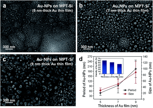 |
| | Fig. 2 (a–c) SEM images of the thermally-dewetted Au-NPs on the surface of MPT-Si samples for different thicknesses (5, 7, and 9 nm) of Au films and (d) estimated average period, size, and density of Au-NPs for the corresponding Au films. | |
Structural and optical properties of the NMDT-Si
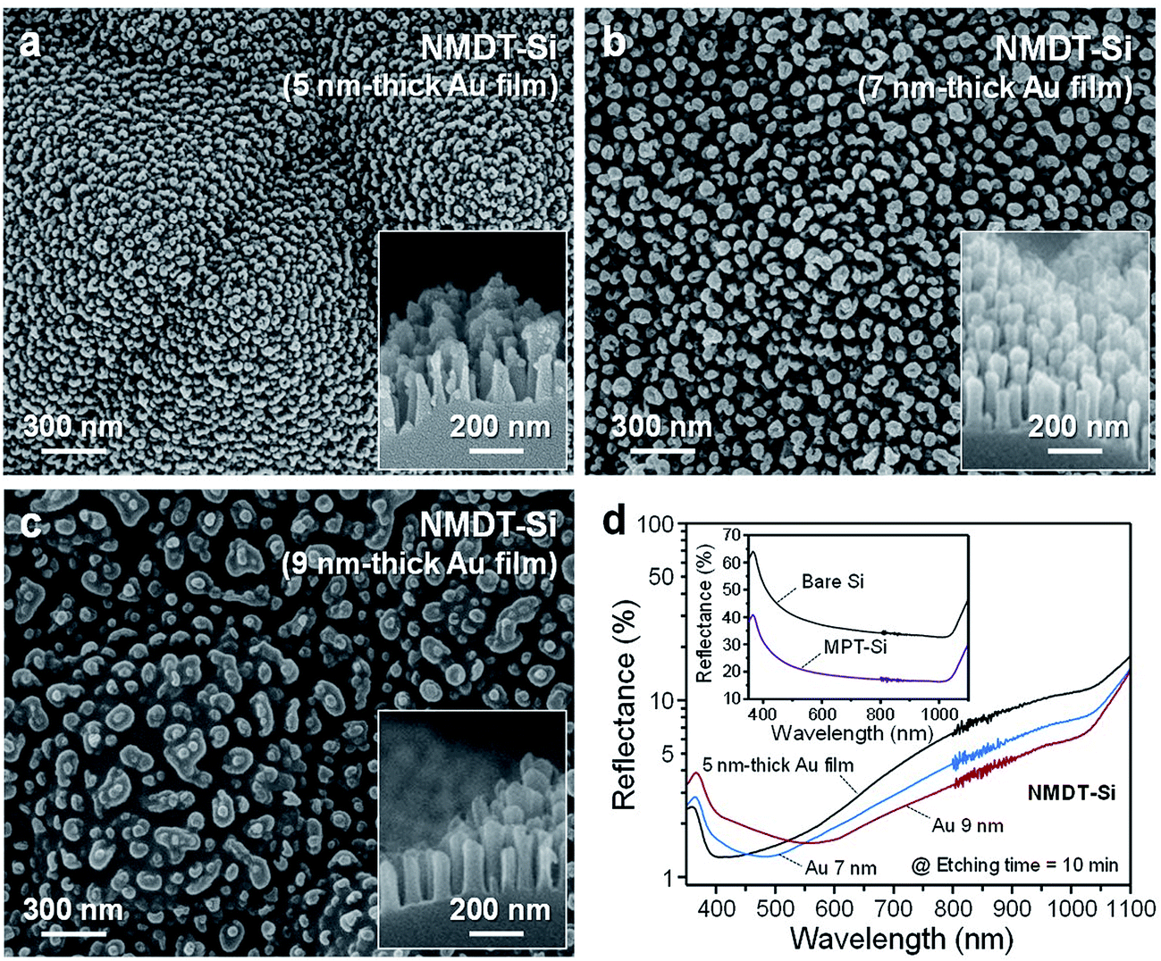
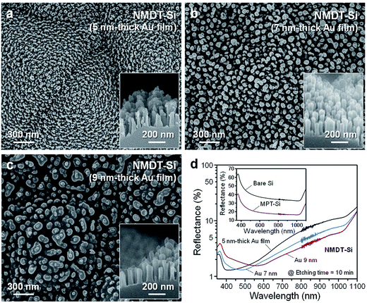
Fig. 3 shows (a–c) the SEM images of NMDT-Si samples for 5, 7, and 9 nm-thick Au films at an etching time of 10 min and (d) the total reflectance spectra of the corresponding samples. For comparison, the reflectance spectra of bare Si and MPT-Si are also shown in the inset of Fig. 3(d). It can be evidently observed that the patterns of Au-NPs are directly transferred onto the surface of MPT-Si by dry etching, which creates the NMDT-Si, as can be seen in Fig. 3(a–c). With increasing the thickness of Au film, the morphology of NTs on the surface of the MPT-Si is changed from the truncated conical pillars to the cylindrical ones, while maintaining the height of ∼200 ± 20 nm without period variation for each Au film. This is the reason why the smaller-sized NPs generated from thinner Au films (e.g., 5 nm) are further quickly eliminated at the edge of NPs compared to the thicker and larger ones during the dry etching. To investigate the effect of NTs with different periods on the reflectance of NMDT-Si samples, their optical reflectance properties were measured in the wavelength range of 350–1100 nm. As shown in Fig. 3(d), the bare Si shows a high surface reflectivity of >30% at wavelengths of 350–1100 nm owing to the large difference in refractive indices between air and the Si, indicating the average reflectance (Ravg) of ∼38.5%. However, the MPTs decrease the reflectance of the bare Si to be Ravg ∼ 20.6% due to the linearly effective graded-refractive-index (GRIN) profile from air to the Si and enhanced light-path lengths caused by the pyramidal micro-structure.20,21 Clearly, an introduction of subwavelength-scale textures (i.e., NTs) into the surface of the MPT-Si leads to the further suppressed reflectivity over a broad wavelength range of 350–1100 nm since they cause not only the additional linearly effective GRIN distribution between air and the surface of MPT-Si, but also allow the only zeroth-order diffracted wave to propagate through the surface of NTs, known as ‘moth eye effect’.22 As the thickness of Au film is increased from 5 to 9 nm, the low reflectance band of the NMDT-Si is shifted towards the longer wavelength region because the period of the NTs becomes larger (i.e., ∼50 ± 15, 90 ± 45, and 200 ± 50 nm for 5, 7, and 9 nm, respectively). Generally, when the grating period becomes much smaller than the wavelength of the incident light, a zeroth-order diffracted light wave is only allowed to reflect (or penetrate) on the grating structure and all the higher orders of diffracted light waves become evanescent, leading to the superior antireflection effect.23,24 This result implies that the low reflectance in a specific wavelength range can be obtained by adjusting the period of NTs (i.e., Au film thickness). For the NMDT-Si at 7 nm-thick Au film, the lowest Ravg of ∼4% is obtained compared to the other samples (Ravg ∼ 5.9 and 4.5% for 5 and 9 nm, respectively).
 |
| | Fig. 3 (a–c) SEM images of NMDT-Si samples for 5, 7, and 9 nm-thick Au films at an etching time of 10 min and (d) total reflectance spectra of the corresponding samples. For comparison, the reflectance spectra of bare Si and MPT-Si are also shown in the inset of (d). | |
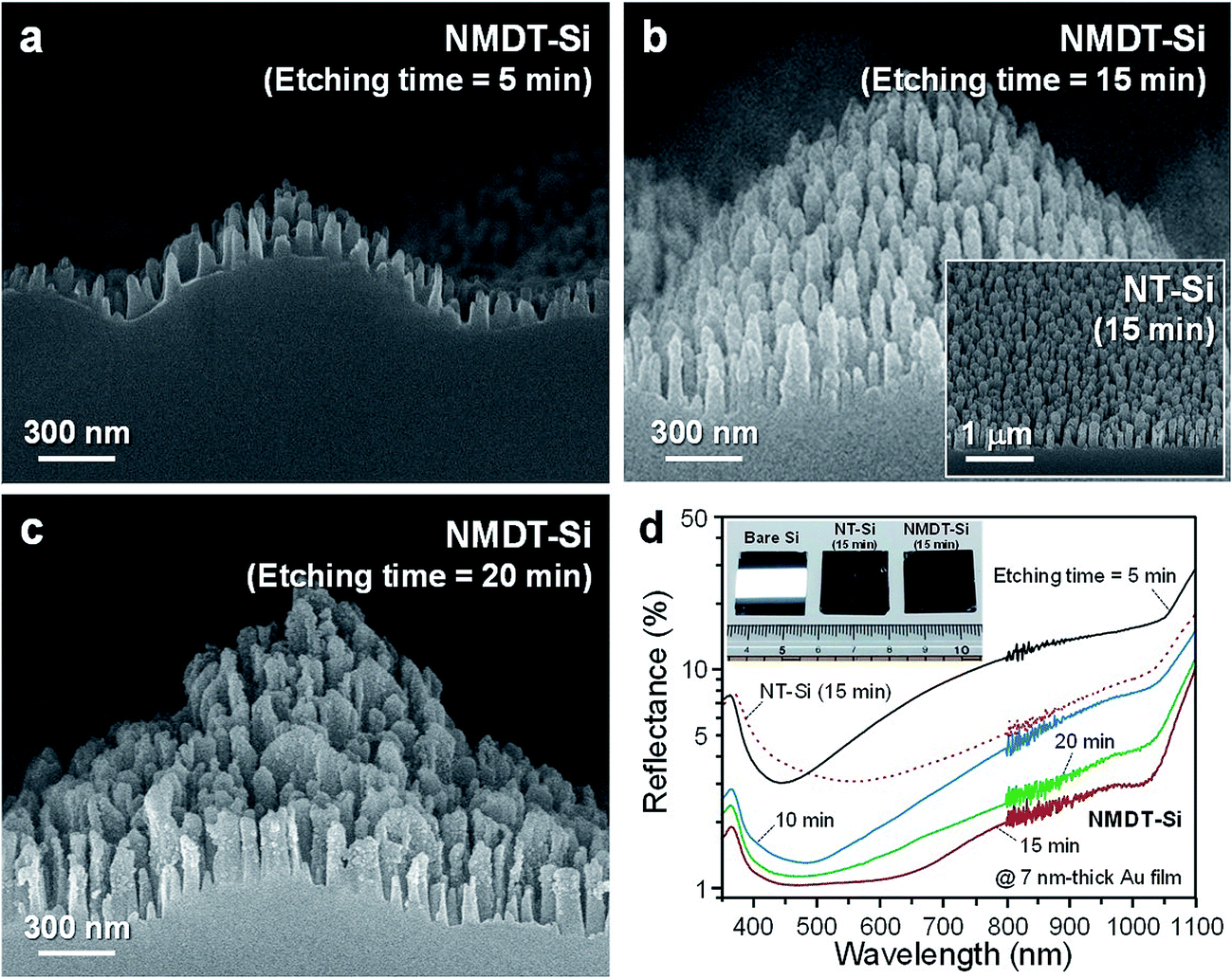
We also investigate the influence of NTs with different heights on the reflectance of NMDT-Si samples. Fig. 4 shows (a–c) the SEM images of NMDT-Si samples at different etching times of 5, 15, and 20 min for 7 nm-thick Au film and (d) the total reflectance spectra of the corresponding samples. For comparison, the SEM image and total reflectance spectrum of the planar NT-Si at 15 min are also shown. As shown in Fig. 4(a–c), the height of NTs on the MPT-Si surface is increased from 100 ± 20 nm at 5 min to 300 ± 30 nm at 15 min while it is contrastively decreased to be 280 ± 40 nm at 20 min, showing the partly collapsed nano-pillars with uneven distributions. This is attributed to the absence of Au-NPs (i.e., complete removal), which are used as an etch mask, at longer etching times. Additionally, the shape of NTs on the MPT-Si surface is varied from the truncated cone at 5 min to the cone at 15 min. As a result, the NMDT-Si consisting of conical NTs with larger heights at 15 min shows the lowest reflectance spectrum (Ravg ∼ 2.1%) compared to the other samples (Ravg ∼ 10 and 2.7% at 5 and 20 min) over a wide wavelength range of 350–1100 nm, as shown in Fig. 4(d). Furthermore, it also exhibits the superior antireflection property in comparison with the planar NT-Si (Ravg ∼ 6%). The outstanding antireflection property can be also confirmed from the photograph in the inset of Fig. 4(d). The fluorescent white light is strongly reflected at the surface of the bare Si. For the planar NT-Si, the faint reflected fluorescent white light is also seen on its surface in spite of a black surface. However, there is no any reflected fluorescent white light on the NMDT-Si with a dark black surface.
 |
| | Fig. 4 (a–c) SEM images of NMDT-Si samples at different etching times of 5, 15, and 20 min for 7 nm-thick Au film and (d) total reflectance spectra of the corresponding samples. For comparison, SEM image and total reflectance spectrum of the planar NT-Si at 15 min are also shown in (b) and (d), respectively. The inset of (d) shows the photographic image of bare Si, NT-Si, and NMDT-Si samples. | |
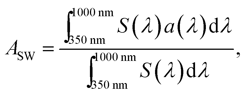
For Si-based solar cell applications, it is necessary to explore the percentage of the incoming solar energy, which is absorbed by the Si, by obtaining the solar weighted absorption (ASW, ratio of the usable photons absorbed to the total usable photons). The ASW can be estimated by normalizing the absorption spectrum with the solar spectral photon flux (i.e., air mass 1.5 global) integrated over a wavelength range of 350–1000 nm.25 The ASW is given by the following equation:
| |
 | (1) |
where
S(
λ) is the spectral photon flux and
a(
λ) is the absorption (100 reflectance–transmittance) of samples at normal incidence. Here, absorption data are not shown and transmittance is zero. As expected, for the NMDT-Si at 15 min, the highest
ASW of ∼98.5% is obtained compared to the other NMDT-Si samples (
ASW ∼ 92.4, 97.2, and 98% at 5, 10, and 20 min, respectively) as well as the bare Si (
ASW ∼ 61.3%), the MPT-Si (
ASW ∼ 79.6%), and the NT-Si (
ASW ∼ 95.7%). These results suggest that the NMDT-Si with the superior antireflection ability can be useful to realize high-performance Si-based photovoltaic systems.
Light-scattering property of the NMDT-Si
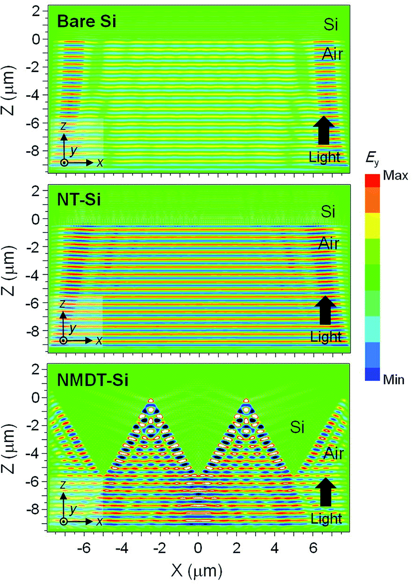
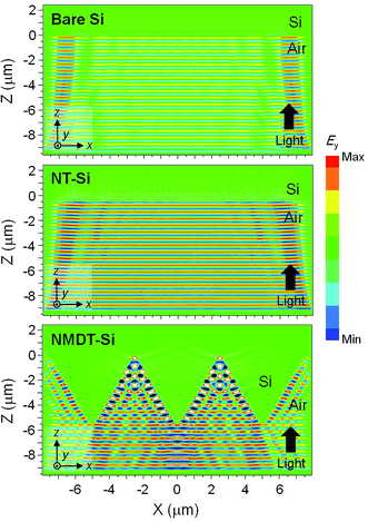
To study the light-scattering propagation of the NMDT-Si with micro-features, the numerical optical analysis was performed using the FDTD method. Fig. 5 shows the contour plots of calculated electric-field intensities for optical light-propagation properties of bare Si, NT-Si, and NMDT-Si via FDTD simulations at λ = 530 nm. As shown in Fig. 5, for both the bare Si and NT-Si, there are no scattered propagating lights inside Si. On the other hand, the NMDT-Si with micro-pyramidal arrays has a strong light scattering property with the wide angular spread due to the extended effective optical path lengths caused by the rebound lights between the micro-pyramids. This implies that the probability of photons transmitted through the surface of the NMDT-Si is increased instead of escaping back to air.6,21
 |
| | Fig. 5 Contour plots of calculated electric-field intensities for optical light-propagation properties of bare Si, NT-Si, and NMDT-Si via numerical FDTD calculations at λ = 530 nm. | |
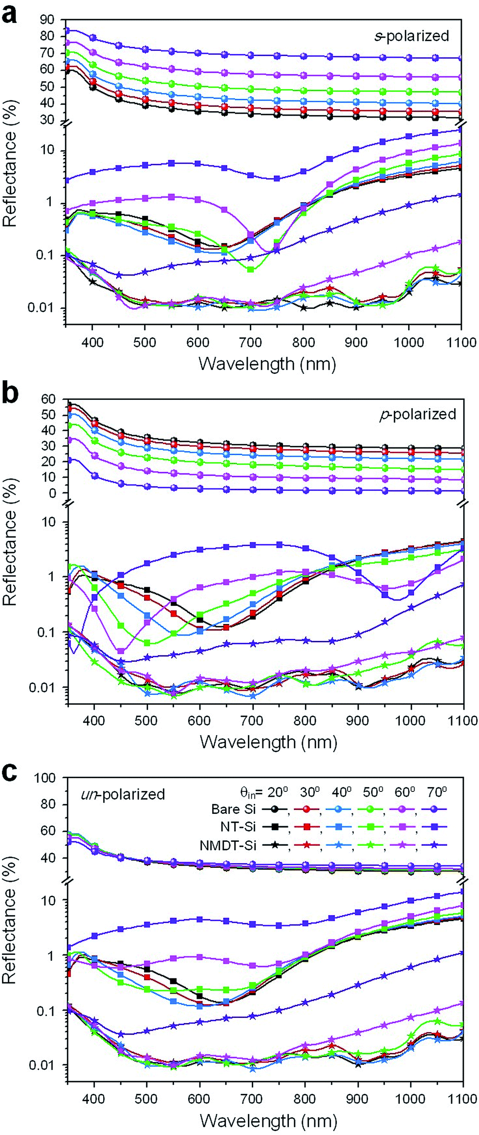
Angle-dependent reflectance characteristics of the NMDT-Si
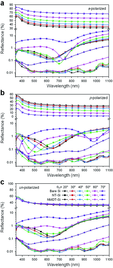
For high-performance devices in optical and optoelectronic applications, the good antireflective characteristics should be obtained in wide angles of incident light for both s- and p-polarized lights. Fig. 6 shows the angle-dependent specular reflectance characteristics of bare Si, NT-Si, and NMDT-Si samples at θin = 20–70° for (a) s-, (b) p-, and (c) un-polarized lights. Here, the NT-Si and NMDT-Si samples fabricated at 7 nm-thick Au film and 15 min-etching time were examined. The bare Si shows strong variations with angles of light incidence for both s- and p-polarized lights. On the other hand, the NT-Si is not relatively sensitive to polarization at θin values lower than 50°, while exhibiting the increased reflectivity with fluctuations at θin ≥ 60°. However, the NMDT-Si has much less angle-dependent reflectance characteristics over wide ranges of wavelengths (350–1100 nm) and incident angles (20–70°), maintaining the reflectance values below 1% for both s- and p-polarized lights. For the un-polarized light in Fig. 6(c), it shows the much lower Ravg of ∼0.06% compared to the bare Si (Ravg ∼ 36.07%) and the NT-Si (Ravg ∼ 2.22%) in the wavelength range of 350–1100 nm at θin = 20–70°.
 |
| | Fig. 6 Angle-dependent specular reflectance characteristics of bare Si, NT-Si, and NMDT-Si samples at θin = 20–70° for (a) s-, (b) p-, and (c) un-polarized lights. | |
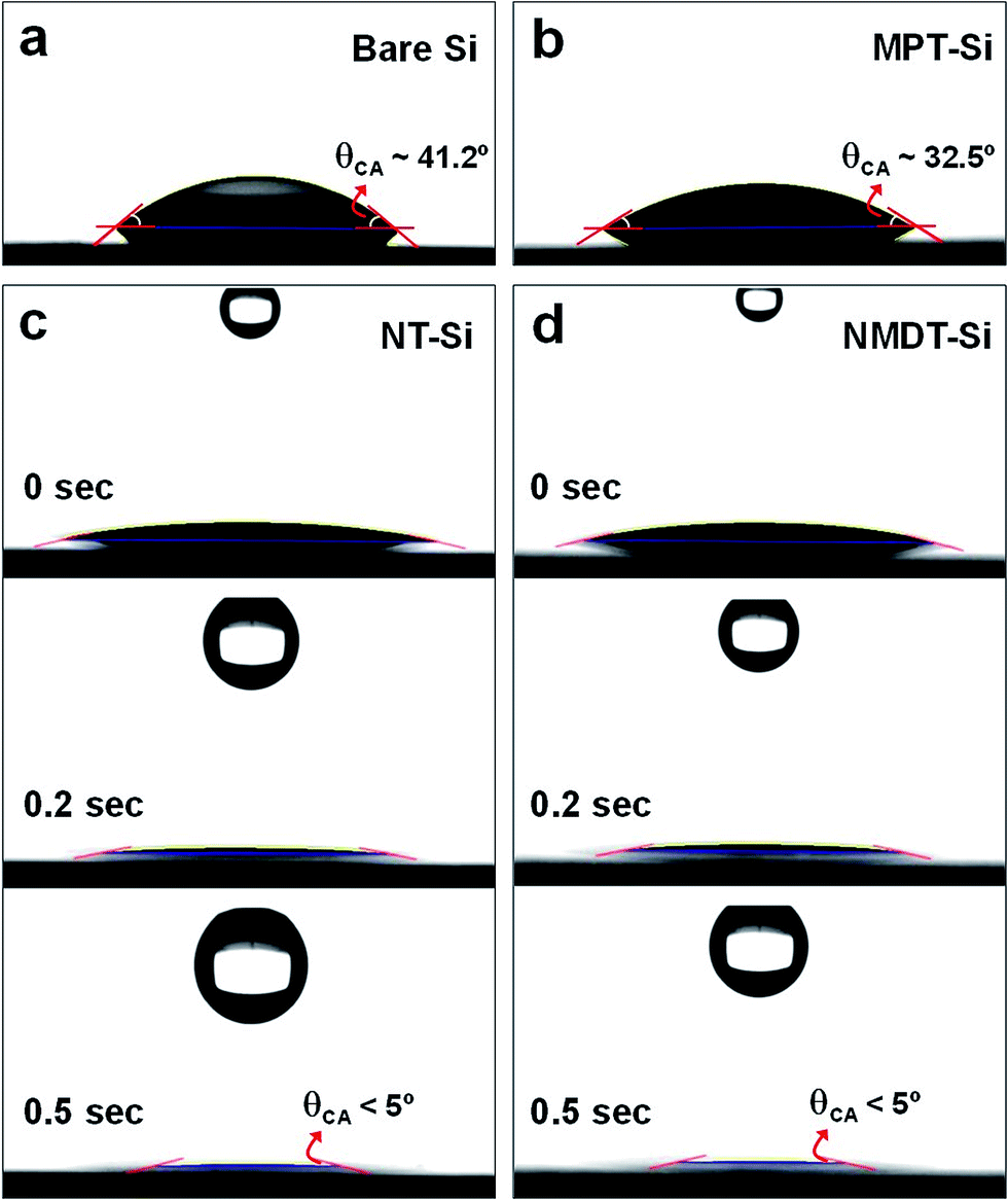
Surface wettability
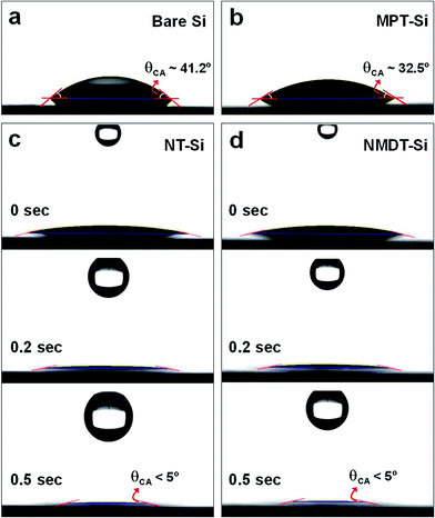
Finally, the surface wetting behaviors of the highly-textured NMDT-Si were studied, compared with the bare Si, MPT-Si, and NT-Si samples. Fig. 7 shows the photographic images of a droplet on the surface of (a) bare Si, (b) MPT-Si, (c) NT-Si, and (d) NMDT-Si samples with each static contact angle value. For both the NT-Si and NMDT-Si at 7 nm-thick Au film and 15 min-etching time, the time-sequential photographic images are also shown. The surface water contact angle (θCA) of MPT-Si is slightly reduced to be ∼32.5° compared to that (θCA ∼ 41.2°) of bare Si, exhibiting the hydrophilic surface. On the other hand, both the NT-Si and NMDT-Si show strong hydrophilic properties with θCA values of <5°. As shown in Fig. 7(c) and (d), a water droplet is immediately spread on the surface like a water sheet film after dropping within 1 s. This complete wetting is attributed to the considerably increased surface roughness due to the NTs, which can be explained by the Wenzel's equation though it is also related to the surface energy of materials and the plasma (ozone) treatment.16,26 The dust particles or contaminants on the super-hydrophilic surface can be easily removed from the surface by the flowing water droplets which can squeeze into the space between the dusts and the surface. Therefore, the NMDT-Si may self-clean the dust particles and quickly dry the rainwater on the surface of Si-based optical and optoelectronic devices in outdoor applications.
 |
| | Fig. 7 Photographic images of a droplet on the surface of (a) bare Si, (b) MPT-Si, (c) NT-Si, and (d) NMDTSi samples with each static contact angle value. For both the NT-Si and NMDT-Si at 7 nm-thick Au film and 15 min-etching time, the time-sequential photographic images are also shown. | |
Conclusions
The outstanding antireflective and hydrophilic architectured Si was fabricated by the nano/micro double-texturing processes. The NMDT-Si was realized by the KOH-based wet etching for the MPTs and the ICP etching via the thermally-dewetted Au-NPs for NTs and their surface morphologies and optical reflectance properties were investigated, together with surface wettability. For the NMDT-Si at 7 nm-thick Au film and 15 min-etching time, surpassing antireflection performance was obtained in broad ranges of wavelengths (350–1100 nm) and incident angles (0–70°) compared to the planar NT-Si as well as the bare Si and the MPT-Si, resulting in the Ravg values of ∼2.1% and ∼0.06% at θin = 0° and 20–70°, respectively. In addition, it strongly scattered the lights penetrated through the surface of NMDT-Si, as confirmed by numerical FDTD simulations. It also had a super-hydrophilic surface with θCA values of <5°. From these results, the nano/micro double-textured Si with high optical light absorption (i.e., efficient antireflection/light-scattering) and self-cleaning ability can be very useful for high-performance Si-based optical and optoelectronic devices.
Acknowledgements
This work was supported by the National Research Foundation of Korea (NRF) Grant funded by the Korea government (MSIP) (No. 2017R1A2B4011998).
Notes and references
- M. L. Brongersma, Y. Cui and S. Fan, Nat. Mater., 2014, 13, 451 CrossRef CAS PubMed; S. F. Leung, Q. Zhang, F. Xiu, D. Yu, J. C. Ho, D. Li and Z. Fan, J. Phys. Chem. Lett., 2014, 5, 1479 CrossRef PubMed; J. W. Leem, M. Choi, D. Bhaskar and J. S. Yu, RSC Adv., 2016, 6, 55159 RSC.
- N. Kadakia, S. Naczas, H. Bakhru and M. Huang, Appl. Phys. Lett., 2010, 97, 191912 CrossRef CAS; C. L. Tien and T. W. Lin, Appl. Opt., 2012, 51, 7229 CrossRef PubMed.
- H. Seidel, L. Csepregi, A. Heuberger and H. Boumgärtel, J. Electrochem. Soc., 1990, 137, 3612 CrossRef CAS; T. Rahman, M. Navarro-Cía and K. Robelets, Nanotechnology, 2014, 25, 485202 CrossRef PubMed.
- B. Dudem, J. H. Heo, J. W. Leem, J. S. Yu and S. H. Im, J. Mater. Chem. A, 2016, 4, 7573 CAS.
- D. Qi, N. Lu, H. Xu, B. Yang, C. Huang, M. Xu, L. Gao, Z. Wang and L. Chi, Langmuir, 2009, 25, 7769 CrossRef CAS PubMed; Y. Jiang, X. Zhang, F. Wang and Y. Zhao, RSC Adv., 2015, 5, 69629 RSC.
- M. Pranaitis, L. Jaraminė, V. Čyras, A. Selskis and A. Galdikas, J. Appl. Phys., 2013, 114, 163523 CrossRef CAS; Y. Song, K. Kim, K. Choi, B. Ki and J. Oh, Sol. Energy, 2016, 135, 291 CrossRef.
- W. R. Wei, M. L. Tsai, S. T. Ho, S. H. Tai, C. R. Ho, S. H. Tsai, C. W. Liu, R. J. Chung and J. H. He, Nano Lett., 2013, 13, 3658 CrossRef CAS PubMed.
- B. Dudem, J. W. Leem, J. H. Lim, S. H. Lee and J. S. Yu, RSC Adv., 2015, 5, 90103 RSC; B. Dudem, Y. H. Ko, J. W. Leem, J. H. Lim and J. S. Yu, ACS Appl. Mater. Interfaces, 2016, 8, 30165 Search PubMed; B. Dudem, J. W. Leem and J. S. Yu, RSC Adv., 2016, 6, 3764 RSC.
- S. A. Boden and D. B. Bagnall, Appl. Phys. Lett., 2008, 93, 133108 CrossRef CAS; Y. M. Song, H. J. Choi, J. S. Yu and Y. T. Lee, Opt. Express, 2010, 18, 13063 CrossRef PubMed; J. W. Leem, S. Kim, S. H. Lee, J. A. Rogers, E. Kim and J. S. Yu, Adv. Energy Mater., 2014, 4, 1301315 CrossRef.
- J. Liu, M. Ashmkhan, G. Dong, B. Wang and F. Yi, Sol. Energy Mater. Sol. Cells, 2013, 108, 93 CrossRef CAS; Y. Cao, A. Liu, H. Li, Y. Liu, F. Qiao, Z. Hu and Y. Sang, Appl. Surf. Sci., 2011, 257, 7411 CrossRef; J. Liu, B. Liu, S. Liu, Z. Shen, C. Li and Y. Xia, Surf. Coat. Technol., 2013, 229, 165 CrossRef; J. Liu, T. Zhang, G. Dong, X. Zhang, B. Wang, Y. Liao and F. Yi, J. Phys. D: Appl. Phys., 2013, 46, 375302 CrossRef.
- J. W. Leem, J. S. Yu, Y. M. Song and Y. T. Lee, Sol. Energy Mater. Sol. Cells, 2011, 95, 669 CrossRef CAS.
- C. I. Yeo, Y. M. Song, S. J. Jang and Y. T. Lee, Opt. Express, 2011, 19, A1109 CrossRef CAS PubMed; J. H. Lim, J. W. Leem and J. S. Yu, RSC Adv., 2015, 5, 61284 RSC.
- G. C. Park, Y. M. Song, J. H. Ha and Y. T. Lee, J. Nanosci. Nanotechnol., 2011, 11, 6152 CrossRef CAS PubMed.
- Y. B. Park, H. Im, M. Im and Y. K. Choi, J. Mater. Chem., 2011, 21, 633 RSC; J. Son, S. Kundu, L. K. Verma, M. Sakhuja, A. J. Danner, C. S. Bhatia and H. Yang, Sol. Energy Mater. Sol. Cells, 2012, 98, 46 CrossRef CAS; J. W. Leem and J. S. Yu, RSC Adv., 2015, 5, 60804 RSC.
- A. B. D. Cassie and S. Baxter, Trans. Faraday Soc., 1944, 40, 546 RSC.
- R. N. Wenzel, Ind. Eng. Chem., 1936, 28, 988 CrossRef CAS.
- J. W. Leem, Y. M. Song and J. S. Yu, Opt. Express, 2011, 19, 26308 CrossRef CAS PubMed.
- SOPRA, N&K Database (2017), retrieved 2017, http://refractiveindex.info.
- P. L. Redmond, A. J. Hallock and L. E. Brus, Nano Lett., 2005, 5, 131 CrossRef CAS PubMed; G. Palasantzas, T. Vystavel, S. A. Koch and J. T. M. De Hosson, J. Appl. Phys., 2006, 99, 024307 CrossRef; H. Chen, Y. Yu, H. L. Xin, K. A. Newton, M. E. Holtz, D. Wang, D. A. Muller, H. D. Abruña and J. DiSalvo, Chem. Mater., 2013, 25, 1436 CrossRef.
- W. H. Southwell, J. Opt. Soc. Am. A, 1991, 8, 549 CrossRef CAS.
- J. Zhao and M. A. Green, IEEE Trans. Electron Devices, 1991, 38, 1925 CrossRef CAS.
- P. B. Clapham and M. C. Hutley, Nature, 1973, 244, 281 CrossRef.
- E. Hecht, Optics, Addison-Wesley, NY, USA, 4th edn, 2002, ch. 10 Search PubMed.
- H. Kikuta, H. Toyota and W. Yu, Opt. Rev., 2003, 10, 63 CrossRef CAS.
- J. W. Leem, S. Kim, C. Park, E. Kim and J. S. Yu, ACS Appl. Mater. Interfaces, 2015, 7, 6706 CAS.
- L. Schneider, M. Laustsen, N. Mandsberg and R. Taboryski, Sci. Rep., 2016, 6, 21400 CrossRef CAS PubMed.
|
| This journal is © The Royal Society of Chemistry 2017 |
Click here to see how this site uses Cookies. View our privacy policy here. 
 Open Access Article
 This Open Access Article is licensed under a
  ,
Bhaskar Dudem and
Jae Su Yu*
,
Bhaskar Dudem and
Jae Su Yu*