
 Open Access Article
 This Open Access Article is licensed under a
 Creative Commons Attribution 3.0 Unported Licence
Evaluation of different buffer materials for solar cells with wide-gap Cu2ZnGeSxSe4−x absorbers†
T. Schnabel *a,
M. Sebouia,
A. Bauera,
L. Choubracb,
L. Arzelb,
S. Harelb,
N. Barreaub and
E. Ahlswedea
*a,
M. Sebouia,
A. Bauera,
L. Choubracb,
L. Arzelb,
S. Harelb,
N. Barreaub and
E. Ahlswedea
aZentrum für Sonnenenergie- und Wasserstoff-Forschung Baden-Württemberg, Meitnerstraße 1, 70563 Stuttgart, Germany. E-mail: thomas.schnabel@zsw-bw.de
bInstitut des Materiaux Jean Rouxel (IMN), Universitéde Nantes, CNRS, 2 rue de la Houssiniere, BP 32229, 44322 Nantes Cedex 03, France
First published on 16th August 2017
Abstract
In this work kesterite-type Cu2ZnGeSxSe4−x (CZGSSe) absorbers were coated with four different buffer layer materials: CdS, In2S3, Zn(O,S) and CdIn2S4. A detailed electrical characterization of the resulting solar cells was performed. The highest open-circuit voltage and the best band alignment could be reached with Zn(O,S), whereas the CdS buffer gave the best efficiencies of up to 6%, which is the highest reported efficiency for a CZGSSe absorber.
Introduction
In recent years, Cu2ZnSnSxSe4−x (CZTSSe) has gained significant attention as an absorber material for thin-film solar cells with the intention to substitute the more mature CuInyGa1−ySe2 (CIGS). However, solar cells with CZTSSe absorber still suffer from a high open-circuit voltage (VOC) deficit that is drastically limiting to the efficiency.One approach to overcome this limitation is the substitution of Ge for Sn which increases the band gap and has been found to improve the crystallinity of the absorber1 and reduce the amount of Sn2+-related defects.2 Significant improvements of VOC and efficiency have been reported for adding a small amount of Ge as dopant.3 For mixed Cu2ZnSnyGe1−ySxSe4−x absorbers efficiencies exceeding 10% have been reported for [Ge]/([Sn] + [Ge])-ratios between 0.25 and 0.4,4–6 some of them with a drastically improved VOC.4 Consequently, the interest in a complete substitution of Ge for Sn is also rising, which allows the possible use as a wide band gap top cell in tandem solar cells with a tunable band gap between 1.4 and 2.0 eV.7,8 So far there are only few manuscripts reporting on the structural and optical characterisation of Cu2ZnGeSxSe4−x (CZGSSe)7,9,10 and some first reports about solar cells.11,12 In previous manuscripts, we could demonstrate efficiencies exceeding 5%.12,13
However, since CdS has a decent spike-like band alignment with CZTSSe14,15 and the conduction band minimum (CBM) of CZGSe was reported to be about 0.5 eV higher than that of CZTSe,16 it is expected to have a non-ideal band alignment with the CZGSSe absorber. In addition for environmental reasons the use of a Cd-free buffer material would be favourable.
Therefore, in this work four different buffer layer materials are compared: CdS, Zn(O,S), In2S3 and CdIn2S4. The first three of them are well-established buffer materials with reported efficiencies for CIGS exceeding 22%,17 21%![[thin space (1/6-em)]](https://www.rsc.org/images/entities/char_2009.gif) 18 and 18%,19 respectively. In contrast, CdIn2S4 is a rather new candidate that was found as reaction product at the interface between CdS and KF-treated CIGS20 and might therefore be linked to the efficiency improvement that is gained from the KF-treatment.
18 and 18%,19 respectively. In contrast, CdIn2S4 is a rather new candidate that was found as reaction product at the interface between CdS and KF-treated CIGS20 and might therefore be linked to the efficiency improvement that is gained from the KF-treatment.
Experimental
The CZGSSe absorbers were prepared from a metal salt solution that consists of copper(I)-chloride (0.46 M), zinc(II)-chloride (0.32 M), germanium(IV)-chloride (0.31 M) and thiourea (1.48 M) with dimethyl formamide as solvent. The chemical composition is chosen to be Cu-poor with metal ratios of Cu/(Zn + Ge) = 0.7 and Zn/Ge = 1.0. The solution is deposited onto a molybdenum-coated soda lime glass substrate by doctor-blade coating and a subsequent drying step. The resulting layer is annealed in Se-atmosphere at 550 °C to exchange S for Se and induce the crystallisation. Further details on the absorber formation can be found in ref. 12.The CdS buffer layer with a thickness of approximately 50 nm was deposited by chemical bath deposition (CBD) from CdSO4, NH4OH and thiourea. Zn(O,S) layers were deposited by sputtering from mixed Zn(O,S) targets with [S]/([S] + [O])-ratios of 0.2 (layer thickness 67 nm) and 0.4 (layer thickness 41 nm). In2S3 layers were grown by atomic layer chemical vapour deposition (ALCVD) at 210 °C from indium(III)-acetylacetonate and hydrogen sulphide. The film thickness was varied between 3 nm and 28 nm by adjusting the number of deposition cycles. To improve the quality of the interface, subsequent heat treatments in ambient atmosphere on a hot plate were performed at temperatures between 180 °C and 220 °C. CdIn2S4 layers were grown by coevaporation of CdS, In and S resulting in a layer thickness of 50 nm.
To obtain functional solar cells, the samples are completed with a sputtered undoped ZnO (i-ZnO, 40 nm) and an aluminium-doped ZnO (ZAO, 400 nm) layer and separated to single cells of 0.25 cm2 each by mechanical scribing. A schematic illustration of the layer stack is displayed in Fig. 1. For samples with a CdIn2S4 buffer, 40 nm of i-ZnO and 180 nm of ZAO were used followed by a Ni/Al/Ni grid, the device area here is 0.5 cm2.
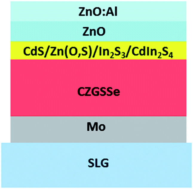 | ||
| Fig. 1 Schematic drawing of the layer stack of a complete solar cell. | ||
Current–voltage curves were measured using a Keithley 2400 source measuring unit under simulated AM 1.5 global solar irradiation with an WACOM 2-lamp sun simulator at 100 mWcm−2. Temperature-dependent current–voltage (JV)-characteristics were measured with a Peltier cooling element in a temperature range from 10 °C (17 °C for CdIn2S4) to 60 °C. External quantum efficiency (EQE) measurements were performed with a setup from Optosolar.
Results
As described in the experimental section, variations of film thickness, heat treatment and composition have been performed for In2S3 and Zn(O,S) buffers. Therefore, these variations are described in the following subsections, before all four buffer materials are compared in the final subsection.In2S3
There are numerous reports about In2S3 as a buffer material for CZTSSe absorbers. For Cu2ZnSnSe4 (CZTSe) efficiencies of 5.7% haven been achieved with In2S3 deposited by co-evaporation21 and spray pyrolysis.22 Risch et al. reported an efficiency of 4.5%, but could achieve a higher VOC in comparison to the CdS-reference. For the Cu2ZnSnS4 (CZTS)–In2S3 interface a spike-like conduction band offset (CBO) of 0.41 eV was reported, which is still in the desired range for high-efficiency solar cells.23 In another work, the VOC was improved by 120 mV in comparison to the CdS-reference. However, due to a very low photocurrent the efficiency was only 0.4%.24 With a sputtered In2S3 buffer on a CZTS absorber both efficiency (4.2%) and VOC (531 mV) were considerably higher than with CdS.25 For a CBD-deposited In2S3 layer an efficiency of 6.9% was reported.26 The highest efficiency with an In2S3 buffer so far is 7.6%, which was achieved with CBD-deposited In2S3 on a CZTSSe absorber.27 Most reports used an additional heat treatment that improved the interface by diffusion of Cu and Na into the buffer and In into the absorber material, respectively.26,28 For CZGSSe absorbers there are no reports about In2S3 buffer layers so far. However, although CZGSSe has a higher band gap, the overall similarity to CZTSSe makes In2S3 a reasonable and interesting choice as buffer material.In Fig. 2 the solar cell parameters of solar cells with In2S3 layer thicknesses from 3 nm to 28 nm are displayed as box plots. Note that these parameters were obtained without an additional heat treatment. For thin In2S3 layers the short circuit current density (JSC) is very low. It strongly increases, until at a film thickness of 7 nm saturation occurs. The VOC reaches its maximum at 7 nm and decreases again for thicker films. For the fill factor (FF) no clear trend is visible with slightly lower values for 5 and 21 nm film thickness. Thus the efficiency reaches its maximum at an In2S3 thickness of only 7 nm with an average value of 2.5%. A comparison with literature is difficult, since most other publications do not report the film thickness. In the case of Jiang et al. it was varied between 50 and 180 nm and was therefore considerably thicker.26
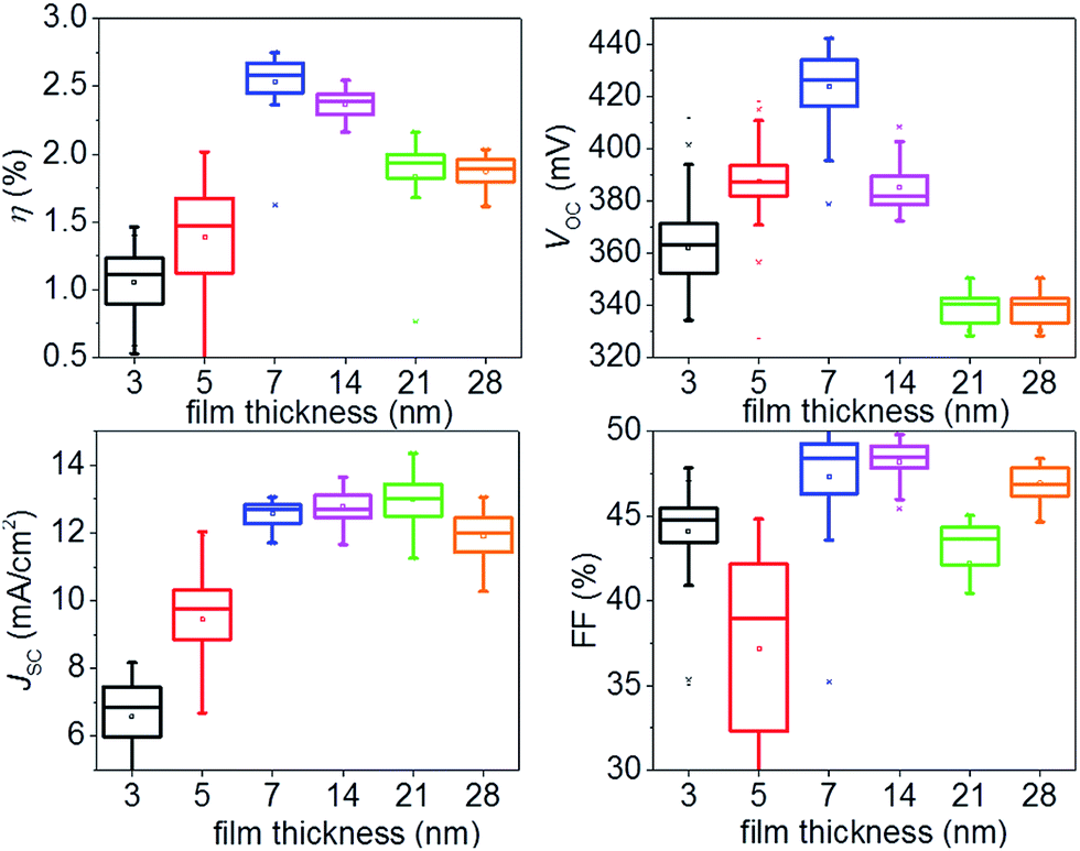 | ||
| Fig. 2 Parameters of solar cells with a CZGSSe absorber and In2S3 buffer with buffer layer thicknesses between 3 and 28 nm. | ||
For the investigation of the effect of post-annealing all samples were subsequently annealed for 15 min on a hot plate in ambient atmosphere at temperatures of 180, 200 and 220 °C. For the sake of clarity, in Table 1 only the results with an In2S3 layer thickness of 7 nm are shown, because they obtained the highest efficiencies. All solar cell parameters are increasing with heating temperature. However, with a gain of 53 mV the effect is most pronounced for VOC whilst the changes in FF and JSC are rather small. The average efficiency after heating at 220 °C is 3.1% with a maximum value of 3.4%. The improvements after post annealing are attributed to diffusion of and Cu and Na into the buffer, which is commonly reported for In2S3 buffers.29 A comparison to other buffer materials will be done later on in this manuscript.
| As grown | 180 °C | 200 °C | 220 °C | |
|---|---|---|---|---|
| η (%) | 2.5 ± 0.2 | 2.7 ± 0.3 | 3.0 ± 0.2 | 3.1 ± 0.3 |
| VOC (mV) | 423 ± 14 | 446 ± 14 | 462 ± 8 | 476 ± 7 |
| JSC (mA cm−2) | 12.6 ± 0.4 | 12.9 ± 0.4 | 13.3 ± 0.5 | 13.2 ± 0.6 |
| FF (%) | 47.3 ± 3.3 | 47.6 ± 3.3 | 49.0 ± 2.0 | 49.9 ± 2.2 |
Zn(O,S)
Zn(O,S) is a promising buffer layer material for solar cells with CZTSSe absorbers since its elements are earth abundant, non-toxic and it offers a higher band gap than CdS which can lead to an increased absorption in the short wavelength regime. The band gap can be tuned from 3.3 eV for pure ZnO to 3.6 eV for pure ZnS with a minimal band gap for 50% ZnO (“bowing”)30 by varying the [S]/([S] + [O])-ratio. This is necessary, because ZnO was reported to have an unfavourable cliff-like CBO with CZTSSe whereas ZnS was found to have a considerably spike-like CBO with a barrier of 1.1 eV.27 Grenet et al. reported an efficiency of 5.8% for a ZnS(O,OH) buffer prepared by CBD.31 The performance is strongly influenced by metastabilities, since “before LS [light soaking] treatment almost no photovoltaic effect is observed”. In a different work, no photocurrent could be obtained for a CZTS absorber and a Zn(O,S) buffer, which is attributed to a high barrier of 0.9 eV at the CBO.24 However, no light soaking was performed. Ericson et al. demonstrated an efficiency of 4.6% for a CZTS/Zn(O,S) system (buffer deposited by ALCVD) with [S]/([S] + [O]) = 0.14 and the activation energy increased with the [S]/([S] + [O])-ratio.32 Recently, Neuschitzer et al. reported an efficiency of 6.5% for CBD-deposited ZnS(O,OH) which is the highest value for a kesterite absorber.33In this work, sputter-deposited Zn(O,S) buffers from mixed targets with [S]/([S] + [O])-ratios of 0.2 and 0.4 are used. These ratios are considerably lower than what is commonly used for CBD-based Zn(O,S) layers for CIGS, where typical [S]/([S] + [O])-ratios are between 0.7 and 0.9.34 However, a direct comparison between sputtering and CBD is different anyway, since depending on the concentration of precursor chemicals with the CBD-approach also Zn(OH)2 species can be formed18 which is not the case for sputtered Zn(O,S).
The JV-characteristics under illumination of solar cells with Zn(O,S) buffers from the targets with [S]/([S] + [O])-ratios of 0.2 and 0.4 are displayed in Fig. 3. The solar cell with a buffer with [S]/([S] + [O]) = 0.2 has an efficiency of 1.4% with VOC = 232 mV, JSC = 14.5 mA cm−2 and FF = 42.1%. In contrast, with [S]/([S] + [O]) = 0.4 an efficiency of 4.6% could be achieved with VOC = 730 mV, JSC = 13.0 mA cm−2, FF = 48.3%. The slightly higher JSC of the sample with [S]/([S] + [O]) = 0.2 can be explained by the higher band gap of the buffer that allows an increased absorption in the short-wave regime. Additionally, the huge difference in VOC is remarkable. It might indicate an improved band alignment and therefore less interface recombination for the Zn(O,S) buffer with higher S-content. However, also other factors such as a different doping of the buffer layer or different tunnel recombination could influence the VOC.
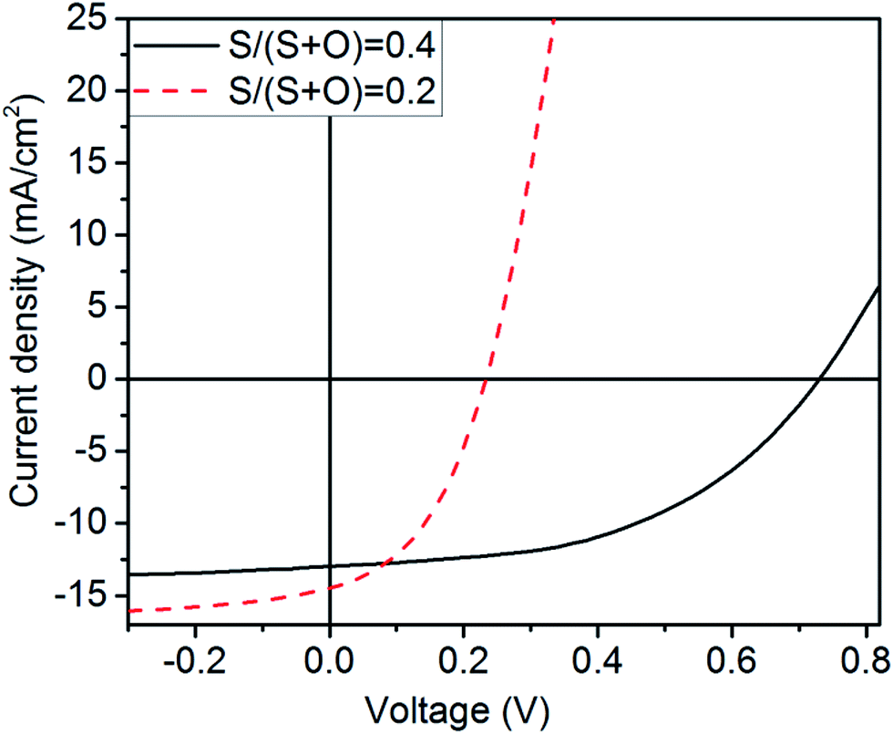 | ||
| Fig. 3 J–V-characteristics of solar cells with Zn(O,S) buffer under illumination. | ||
Note that in contrast to some of the previously cited reports, no improvement of the solar cell efficiency was obtained after light soaking. However, this is not surprising since the J–V-characteristics do not have a kink as it was reported by Neuschitzer et al. before light soaking.33
Comparison
In this section the best sample types from each buffer material are compared. In detail that are (i) sputtered Zn(O,S) with [S]/([S] + [O]) = 0.4 and a thickness of 40 nm, (ii) CBD-deposited CdS with a thickness of approximately 50 nm, (iii) ALCVD-deposited In2S3 with a thickness of 7 nm and a subsequent heat treatment for 15 min at 180 °C on a hot plate and (iv) coevaporated CdIn2S4 with a thickness of 50 nm.The solar cell parameters for all buffer materials are compared as box plots in Fig. 4. In terms of efficiency, solar cells with a CdS buffer clearly show the best performance with an average value of 5%. All other materials only show average efficiencies around 3%. However, solar cells with a Zn(O,S) buffer could achieve VOC-values of up to 733 mV which is clearly higher than all other buffer materials and indicates an improved absorber–buffer-interface. The average VOC for In2S3 and CdIn2S4 is 475 mV and 350 mV, respectively. On the other hand, Zn(O,S) exhibits the lowest FF (37% in comparison to around 50% for the other materials) and JSC (10.5 mA cm−2 in comparison to between 13 and 15 mA cm−2 for the other materials). Especially in the case of JSC this is surprising, since the used Zn(O,S) should have a band gap of around 2.6 eV35 which is higher than that of CdS and should therefore allow an increased absorption of photons in the short wavelength regime.
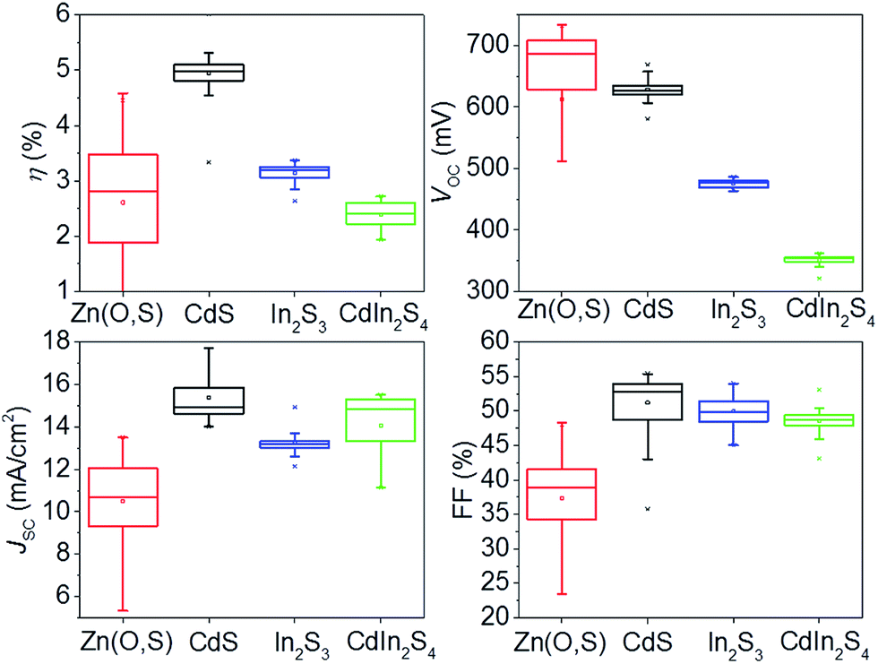 | ||
| Fig. 4 Parameters of solar cells with a CZGSSe absorber and different buffer materials. | ||
To investigate this in more detail, EQE measurements were performed (Fig. 5). In the short wavelength region the sample with CdIn2S4 buffer shows by far the lowest absorption. On the contrary, the sample with Zn(O,S) buffer indeed shows a considerably increased absorption between 400 and 500 nm in comparison to the CdS buffer. The same holds true for the sample with In2S3 buffer. Note that according to literature the band gap of In2S3 was found to vary between 2.25 eV and 3.2 eV depending on the deposition technique used.36 For films by ALCVD it was found to be 2.7 eV37 and thus the increased absorption in the short wavelength regime is expected. It may additionally be mentioned that the very low film thickness of 7 nm also affects the absorption.
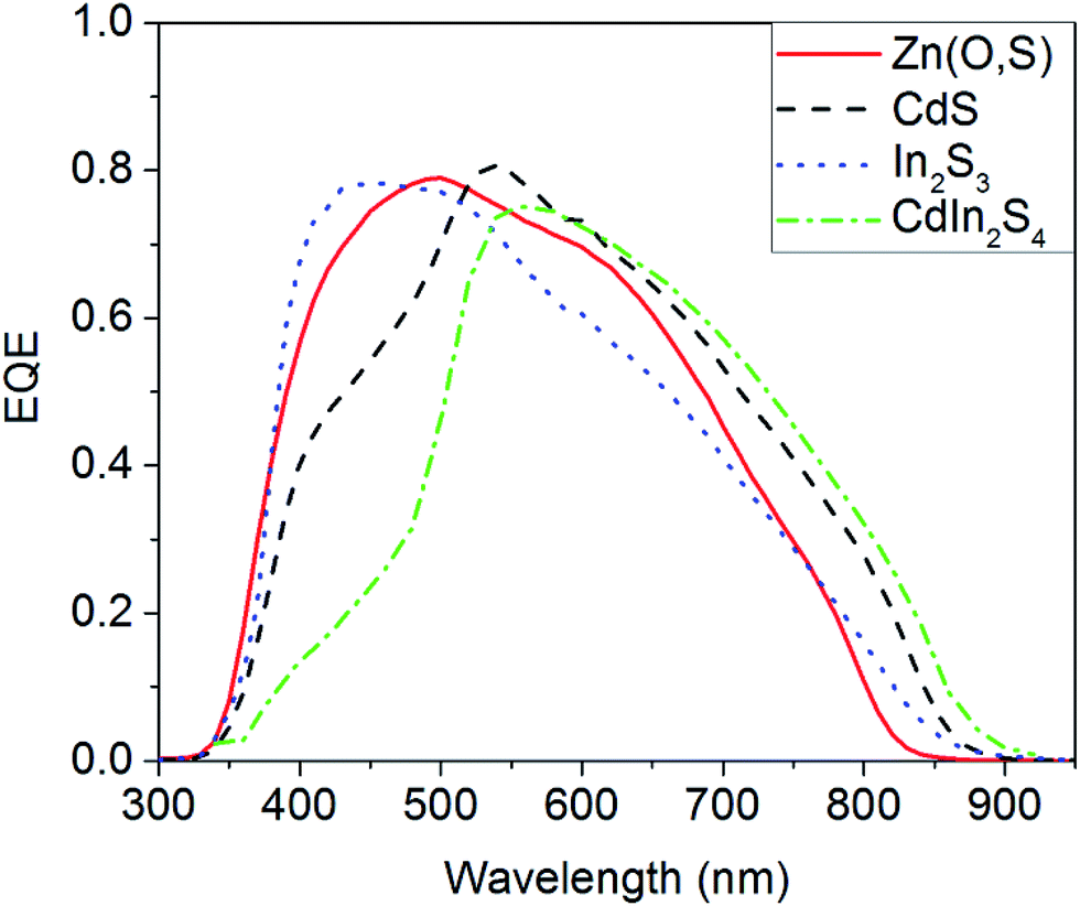 | ||
| Fig. 5 EQE measurements of solar cells with CZGSSe absorber and different buffer layers. | ||
However, both Zn(O,S) and In2S3 suffer from strongly decreased collection in the long wavelength regime in comparison to CdS and CdIn2S4. For this behaviour two possible reasons can be found. On the one hand, (i) CBD-deposited CdS is usually present not only at the interface, but also in the bulk of the absorber, where it can reach through small pinholes. There it is able to passivate grain boundaries which facilitates the electron transport and is beneficial for the carrier collection.38
On the other hand, (ii) the band gaps of the absorber layers discussed in this manuscript are found to be slightly different. A linear extrapolation from the squared plot of the EQE (see ESI†) suggests 1.44 eV with CdIn2S4 buffer, 1.47 eV with CdS and 1.54 eV with Zn(O,S). For the In2S3 buffer the plot is not linear, which can be attributed to strong band tailing. Thus only a range between 1.49 and 1.54 eV can be given. The reasons for this differences are not understood in detail yet. However, they might be linked to diffusion of Cd into the kesterite absorber, which can replace Zn and thereby decrease the band gap.39 This might explain the higher band gaps of CZGSSe absorbers with Cd-free buffer materials. Consequently, the increased absorption in the long wavelength regime with a CdIn2S4 buffer could be explained by the lower band gap of the corresponding absorber.
To gain further understanding about the absorber–buffer-interface, temperature-dependent JV characteristics were measured in a temperature range between 10 °C (17 °C for CdIn2S4) and 60 °C. From a linear extrapolation of the plot of VOC versus temperature to 0 K the activation energy of the dominant recombination path (EA) can be estimated. If it is smaller than the band gap, this is indicative of dominant interface recombination.40,41 The results are displayed in Table 2. The activation energies for all buffer materials are smaller than the band gap of the CZGSSe absorber, thus all solar cells should be limited by interface recombination. However, there are still distinct differences between the different buffer materials.
| EG (eV) | VOC (mV) | EG/q − VOC (mV) | EA (meV) | EG − EA (meV) | η (%) | |
|---|---|---|---|---|---|---|
| Zn(O,S) | 1.54 | 730 | 810 | 1307 | 233 | 4.6 |
| CdS | 1.47 | 617 | 853 | 1277 | 193 | 6.0 |
| In2S3 | 1.49–1.54 | 469 | 1021–1071 | 1115 | 375–425 | 3.4 |
| CdIn2S4 | 1.44 | 354 | 1086 | 820 | 620 | 2.6 |
Since the band gaps are slightly different, the difference between EG and EA was calculated to allow a better comparison. Here with 193 meV the CdS buffer shows the lowest difference indicating the best absorber–buffer interface. The Zn(O,S) buffer only has a slightly higher difference between EG and EA (233 meV) whereas In2S3 and CdIn2S4 seem to have a considerably lower interface quality.
However, another option to compare the different buffer materials is the VOC-deficit EG − VOC that is also displayed in Table 2. In this case we get a slightly different picture, since Zn(O,S) has the lowest VOC-deficit of 810 mV (which is, of course, still very high). The CdS buffer shows a slightly higher VOC-deficit of 853 mV, while In2S3 and CdIn2S4 have values above 1 eV.
In summary, the comparison of EG − EA and VOC-deficit suggests an apparent contradiction since either Zn(O,S) or CdS seem to have the best interface quality of the investigated buffer materials. For further increasing the solar cell efficiency the most crucial factor is the absorber itself which has to be optimized. For an improved buffer layer a combination of a very thin CdS-layer by CBD to passivate defects in the bulk and a Zn(O,S) layer on top might be interesting. A similar “hybrid buffer” has been reported for a combination of CdS and In2S3 where considerable improvements in VOC and efficiency could be obtained.42,43
Conclusions
Thin-film solar cells with a wide-gap kesterite CZGSSe absorber and four different buffer layers, namely CdS, Zn(O,S), In2S3 and CdIn2S4, have been prepared. All buffer materials resulted in functional devices. For In2S3 different film thicknesses were compared with the best efficiency of 3.4% for an only 7 nm thick buffer layer. The best working device was prepared with a CdS buffer and resulted in an efficiency of 6.0%, which is the highest value for CZGSSe absorbers. However, with Zn(O,S) a higher open circuit voltage and a higher activation energy of the dominant recombination path could be obtained, which indicates a better band alignment compared to CdS.Conflicts of interest
There are no conflicts of interest to declare.Acknowledgements
The authors thank Guy Brammertz and Bart Vermang for fruitful discussions. This work was performed within the SWInG project that has received funding from the European Union's Horizon 2020 research and innovation programme under grant agreement No. 640868.Notes and references
- D. B. Khadka and J. Kim, J. Phys. Chem. C, 2015, 119, 1706–1713 CAS.
- T. J. Huang, X. Yin, G. Qi and H. Gong, Phys. Status Solidi RRL, 2014, 8, 735–762 CrossRef CAS.
- S. Giraldo, M. Neuschitzer, T. Thersleff, S. Lopez-Marino, Y. Sanchez, H. Xie, M. Colina, M. Placidi, P. Pistor, V. Izquierdo-Roca, K. Leifer, A. Perez-Rodriguez and E. Saucedo, Adv. Energy Mater., 2015, 5, 1501070 CrossRef.
- A. D. Collord and H. W. Hillhouse, Chem. Mater., 2016, 28, 2067–2073 CrossRef CAS.
- E. Garcia-Llamas, J. M. Merino, R. Serna, X. Fontane, I. A. Victorov, A. Perez-Rodriguez, M. Leon, I. V. Bodnar, V. Izquierdo-Roca and R. Caballero, Sol. Energy Mater. Sol. Cells, 2015, 158, 147–153 CrossRef.
- Q. Guo, G. M. Ford, W. Yang, C. J. Hages, H. W. Hillhouse and R. Agrawal, Sol. Energy Mater. Sol. Cells, 2012, 105, 132–136 CrossRef CAS.
- D. B. Khadka and J. Kim, CrystEngComm, 2013, 15, 10500–10509 RSC.
- L. Huang, H. Deng, J. He, X. Meng, J. Tao, H. Cao, L. Sun, P. Yang and J. Chu, Mater. Lett., 2015, 159, 1–4 CrossRef CAS.
- M. Buffiere, H. ElAnzeery, S. Oueslati, K. Ben Messaoud, G. Brammertz, M. Meuris and J. Poortmans, Thin Solid Films, 2015, 582, 171–175 CrossRef CAS.
- H. Matsushita, T. Ochiai and A. Katsui, J. Cryst. Growth, 2005, 275, e995–e999 CrossRef CAS.
- K. Timmo, M. Kauk-Kuusik, M. Altosaar, J. Raudoja, T. Raadik, M. Grossberg, T. Varema, M. Pilvet, I. Leinemann, O. Volobujeva and E. Mellikov, 28th European Photovoltaic Solar Energy Conference and Exhibition, 2013 Search PubMed.
- T. Schnabel, M. Seboui and E. Ahlswede, RSC Adv., 2017, 7, 26–30 RSC.
- S. Sahayaraj, G. Brammertz, B. Vermang, T. Schnabel, E. Ahlswede, Z. Huang, S. Ranjbar, M. Meuris, J. Vleugels, J. Poortmans and G. Brammertz, Sol. Energy Mater. Sol. Cells, 2017, 171, 136–141 CrossRef CAS.
- J. Li, M. Wei, Q. Du, W. Liu, G. Jiang and C. Zhu, Surf. Interface Anal., 2013, 45, 682–684 CrossRef CAS.
- R. Haight, A. Barkhouse, O. Gunawan, B. Shin, M. Copel, M. Hopstaken and D. B. Mitzi, Appl. Phys. Lett., 2011, 98, 253502 CrossRef.
- Q. Shu, J. Yang, S. Chen, B. Huang, H. Xiang, X. Gong and S. Wei, Phys. Rev. B: Condens. Matter Mater. Phys., 2013, 87, 115208 CrossRef.
- P. Jackson, R. Wuerz, D. Hariskos, E. Lotter, W. Witte and M. Powalla, Phys. Status Solidi RRL, 2016, 10, 583–586 CrossRef CAS.
- D. Hariskos, P. Jackson, W. Hempel, S. Paetel, S. Spiering, R. Menner, W. Wischmann and M. Powalla, IEEE J. Photovolt., 2016, 6, 1321–1326 CrossRef.
- S. Spiering, A. Nowitzki, F. Kessler, M. Igalson and H. Abdel Maksoud, Sol. Energy Mater. Sol. Cells, 2016, 144, 544–550 CrossRef CAS.
- E. Gautron, T. Lepetit, S. Harel, L. Arzel, L. Assmann, A. Frelon, R. Andrade, S. Sadewasser, T. Douillard and T. Epicier, Heterointerfaces TEM characterization of buffer layers in KF treated CIGS solar cells. Towards a new buffer layer?, European Microscopy Congress, 2016, p. 898 Search PubMed.
- M. Buffiere, G. Brammertz, S. Sahayaraj, M. Meuris, J. Poortmans and N. Barreau, IEEE Phot. Spec. Conf., 2015 Search PubMed.
- D. B. Khadka, S. Kim and J. Kim, J. Phys. Chem. C, 2015, 119, 12226–12235 CAS.
- X. Liu, Y. Feng, H. Cui, F. Liu, X. Hao, G. Conibeer, D. B. Mitzi and M. Green, Prog. Photovoltaics, 2016, 24, 879–898 Search PubMed.
- C. Yan, F. Liu, N. Song, B. K. Ng, J. A. Stride, A. Tadich and X. Hao, Appl. Phys. Lett., 2014, 104, 173901 CrossRef.
- P. Bras and J. Sterner, IEEE Phot. Spec. Conf., 2014 Search PubMed.
- F. Jiang, C. Ozaki, O. Gunawan, T. Harada, Z. Tang, T. Minemoto, Y. Nose and S. Ikeda, Chem. Mater., 2016, 28, 3283–3291 CrossRef CAS.
- D. A. R. Barkhouse, R. Haight, N. Sakai, H. Hiroi, H. Sugimoto and D. B. Mitzi, Appl. Phys. Lett., 2012, 100, 193904 CrossRef.
- D. Hariskos, S. Spiering and M. Powalla, Thin Solid Films, 2005, 480, 99–109 CrossRef.
- S. Spiering, L. Bürkert, D. Hariskos, M. Powalla, B. Dimmler, C. Giesen and M. Heuken, Thin Solid Films, 2009, 517, 2328–2331 CrossRef CAS.
- M. Buffiere, S. Harel, C. Guillot-Deudon, L. Arzel, N. Barreau and J. Kessler, Phys. Status Solidi A, 2014, 212, 282–290 CrossRef.
- L. Grenet, P. Grondin, K. Coumert, N. Karst, F. Emieux, F. Roux, R. Fillon, G. Altamura, H. Fournier and P. Faucherand, Thin Solid Films, 2014, 564, 375–378 CrossRef CAS.
- T. Ericson, J. J. Scragg, A. Hultqvist, J. T. Watjen, P. Szaniawski, T. Torndahl and C. Platzer-Bjorkman, IEEE J. Photovolt., 2014, 4, 465–469 CrossRef.
- E. Saucedo, A. Perez-Rodriguez, M. Neuschitzer and K. Lienau, J. Phys. D: Appl. Phys., 2016, 49, 125602 CrossRef.
- D. Hariskos, R. Menner, P. Jackson, S. Paetel, W. Witte, W. Wischmann, M. Powalla, L. Bürkert, T. Kolb, M. Oertel, B. Dimmler and B. Fuchs, Prog. Photovoltaics, 2012, 20, 534–542 CAS.
- A. Polity, B. K. Meyer, T. Krämer, C. Wang, U. Haboeck and A. Hoffmann, Phys. Status Solidi A, 2006, 203, 2867–2872 CrossRef CAS.
- F. Mesa, W. Chamorro and M. Hurtado, Appl. Surf. Sci., 2015, 350, 38–42 CrossRef CAS.
- S. Spiering, D. Hariskos, M. Powalla, N. Naghavi and D. Lincot, Thin Solid Films, 2003, 431, 359–363 CrossRef.
- M. Werner, D. Keller, S. G. Haass, C. Gretener, B. Bissig, P. Fuchs, F. La Mattina, R. Erni, Y. E. Romanyuk and A. N. Tiwari, ACS Appl. Mater. Interfaces, 2015, 7, 12141–12146 CAS.
- M. Altosaar, J. Raudoja, K. Timmo, M. Danilson, M. Grossberg, J. Krustok and E. Mellikov, Phys. Status Solidi A, 2008, 205, 167–170 CrossRef CAS.
- V. Nadenau, U. Rau, A. Jasenek and H. W. Schock, J. Appl. Phys., 2000, 87, 584–593 CrossRef CAS.
- M. Turcu, O. Pakma and U. Rau, Appl. Phys. Lett., 2002, 80, 2598 CrossRef CAS.
- H. Hiroi, N. Sakai, T. Kato, and H. Sugimoto, IEEE Phot. Spec. Conf., 2013 Search PubMed.
- C. Yan, F. Liu, K. Sun, N. Song, J. A. Stride, F. Zhou, X. Hao and M. Green, Sol. Energy Mater. Sol. Cells, 2016, 144, 700–706 CrossRef CAS.
Footnote |
| † Electronic supplementary information (ESI) available. See DOI: 10.1039/c7ra06438a |
| This journal is © The Royal Society of Chemistry 2017 |