
 Open Access Article
 This Open Access Article is licensed under a
 Creative Commons Attribution 3.0 Unported Licence
The interface degradation of planar organic–inorganic perovskite solar cell traced by light beam induced current (LBIC)†
Yanqing Yaoab,
Gang Wangab,
Fei Wuab,
Debei Liuab,
Chunyan Linab,
Xi Raoab,
Rong Wuc,
Guangdong Zhouab and
Qunliang Song *ab
*ab
aInstitute for Clean Energy and Advanced Materials, Faculty of Materials and Energy, Southwest University, Chongqing 400715, P. R. China. E-mail: qlsong@swu.edu.cn
bChongqing Key Laboratory for Advanced Materials and Technologies of Clean Energy, Chongqing 400715, P. R. China
cKey Laboratory of Solid-State Physics and Devices, School of Physical Science and Technology, Xinjiang University, Urumqi 830046, China
First published on 5th September 2017
Abstract
The light beam induced current (LBIC) method was adopted to nondestructively map the photoresponse of real planar organic–inorganic hybrid perovskite solar cells (PSCs). It is found that the photoresponse of the devices is not uniform even though the morphology of the perovskite films from scanning electron microscope (SEM) or atomic force microscope (AFM) images shows uniform character. This nonuniformity of the photoresponse of the devices is further exacerbated after degradation, which can be well traced by the LBIC method. The indistinguishable morphology change during the device degradation indicates that the degradation of the device is not mainly determined by the morphology of the perovskite layer, but by the interface between the perovskite and the electrode. By using the LBIC method, the worse performing area of the device is identified and then removed accordingly. The current density of the device can be enhanced from 19.44 mA cm−2 to 21.72 mA cm−2 after this clearance of the worse performing area.
Introduction
The power conversion efficiency (PCE) of hybrid organic–inorganic perovskite solar cells has rocketed to as high as 22.1% since they were discovered in 2009.1–10 Due to their advantages of low cost of solution process and high performance, PSCs have great potential for commercialization.11 Since the issue of stability is crucial to deliver PSC technology for commercialization,12 the perovskite layer becomes the core of the device and its stability is believed to be the most important. The stability of perovskite film can be described as unchanged by the film morphology on one hand.13 On the other hand, the stability of the perovskite layer also can be presented as energy disorder/traps. Defects or traps normally exist in the perovskite layer and also at the interfaces,14 caused by the low temperature solution fabrication process and weak chemical bonding among the atoms. Thus to obtain a stable device with high PCE, both the film morphology and defects are ideally unchanged after long term illumination. Indeed, by using new fabrication method15–17 or adjusting the component of precursor,18,19 the more smooth and compact perovskite films, which can be characterized by scanning electron microscope (SEM) or atomic force microscope (AFM), are obtained and the PCE are subsequently improved. SEM and AFM are also powerful tools to figure out the influence of parameters e.g. solvent volatilization,20 annealing temperature,21 and thickness of the film,17 etc. on the size of perovskite crystalline and film coverage.7,22 However, interfaces are also reported to be one of the most important factors for intrinsic stability of PSC.23 Defects or energy disorder at the interfaces can greatly determine the device performance. Generally, SEM and AFM are conducted on a very small area of a partial device, i.e. perovskite films without top selective electrode. Thus the morphology images can not correspond to the photoresponse of a real device including interfaces. The discrepancy between the morphology stability and the device performance stability is more prominent if the device degradation is mostly caused by defects introduced at interfaces. It is known that perovskite materials are relatively stable (storage in glove box) compared to perovskite solar cells.24–27 This means after certain time of storage the device performance decreases a lot though the film morphology is not changed significantly. Thus to characterize the photoresponse of a real device, especially to trace its degradation, a more direct method such as light beam induced current (LBIC) must be used. The LBIC method is a non-destructive characterization technique which has been widely used to diagnose and trace the degradation processes of organic and inorganic photovoltaic devices.28–30 In this characterization technique, a light beam with very small size is used to obtain a photo-response mapping which depicts the cell's current response as a function of beam position. Recently, LBIC has also been mainly introduced in characterizing perovskite solar cells with mesoporous structure, while only a few works of that with planar structure are reported.31–37 With the combination of other characterization techniques, the important features such as crystalline size,33 humidity,34 solvent,35 charge injection at interface,36 etc. could be identified. However, very limited references31,32 corresponding to planar structure perovskite solar cells focuses on interfacial barrier/contact study.In this paper, the LBIC method is used to map and trace the degradation of planar perovskite solar cells. To the best of our knowledge, there is no study on degradation of planar perovskite solar cells by using LBIC. Compared with mesoporous structure, the thickness of perovskite layer in planar structure is more uniform. The results show that though the morphology obtained from SEM/AFM images are uniform as expected, the photoresponse from LBIC is nonuniform. The light conversion efficiency decreases after certain time of storage. The LBIC results record this fast degradation, sharp contrast to the indiscernible change of morphology obtained by SEM/AFM. The worse performance area of the device was identified by LBIC technique and then removed. The PCE of the device can be enhanced from 10.88% to 11.58% after this removal. Thus the gradually introduced defects and the degradation of interfaces are attributed to the fast performance decrease of perovskite solar cells rather than the morphology of perovskite layer.
Experimental details
Materials
Lead chloride (PbCl2), methyl ammonium iodide (MAI), phenyl-C61-butyric acid methyl ester (PCBM), poly(3,4-ethylenedioxythiophene) poly(styrenesulfonate) (PEDOT:PSS) were all purchased from Xi'an Polymer Light Technology Corp (China), while N,N-dimethylformamide (DMF), chlorobenzene and others were from Sigma-Aldrich. The mixed-halide perovskite precursor (CH3NH3PbI3−xClx) and TiO2 precursor were prepared according to literatures procedure.38,39 MAI and PbCl2 were dissolved in DMF at 3![[thin space (1/6-em)]](https://www.rsc.org/images/entities/char_2009.gif) :1 molar ratio with a concentration of 2.4 M MAI and 0.8 M PbCl2 and stirred overnight at room temperature. 20 mg PCBM was dissolved in 1 ml chlorobenzene and stirred overnight at room temperature.
:1 molar ratio with a concentration of 2.4 M MAI and 0.8 M PbCl2 and stirred overnight at room temperature. 20 mg PCBM was dissolved in 1 ml chlorobenzene and stirred overnight at room temperature.
Device fabrication
The structure of the perovskite solar cells was ITO/PEDOT:PSS/CH3NH3PbI3−xClx/PCBM/C60/Al. The fabrication method was reported elsewhere.40 Another structure of the perovskite solar cells was FTO/TiO2/CH3NH3PbI3−xClx/spiro-OMeTAD/Ag. The detail steps were reported in literature.39 The cell area, defined as the cross area between the ITO/FTO and Al/Ag electrode, was 0.09 cm2.LBIC setup
The setup of the homemade LBIC33,35,41 is shown in Fig. 1a. The device was fixed on motorized moving system (TSA30-C, Zolix Beijing China) together with its controller (SC300, Zolix Beijing China), which is used to map the device. A 405 nm laser (Cobolt 06-01, spectral bandwidth < 1.2 nm) was used as the light source, which was further focused in the glove box by lens. The photocurrent induced by the small light beam was then recorded by the current recorder (electrochemical workstation, CHI600D).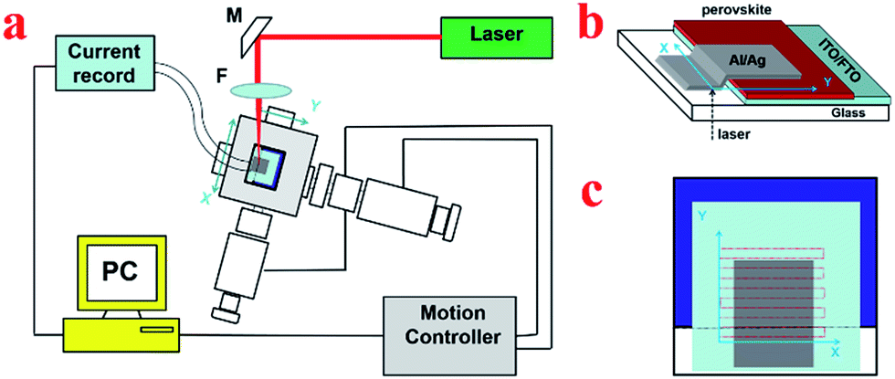 | ||
| Fig. 1 (a) Schematic diagram of LBIC setup. M – turning mirror, F – microscope objective lens. (b) Schematic diagram of scanning. (c) Scanning-path of the laser. | ||
Other characterizations
The morphologies of the developed structures were examined using field-emission scanning electron microscopy (SEM, JSM-6700F) and atomic force microscope (AFM, Dimension Icon). The J–V characteristics of the developed devices were measured using Keithley 2400 in conjunction with Newport 94043A solar simulator, which generated 100 mW cm−2 (AM 1.5 G) simulated sunlight. The external quantum efficiency (EQE) of the devices was calculated from the photocurrent measured using a lock-in amplifier (SR-830). After fabrication, all the J–V, EQE and LBIC mapping characteristics were measured in the glove box.Results and discussion
The P–I–N and N–I–P structures of the perovskite solar cells are ITO/PEDOT:PSS/CH3NH3PbI3−xClx/PCBM/C60/Al and FTO/TiO2/CH3NH3PbI3−xClx/spiro-OMeTAD/Ag, respectively, as shown in Fig. 2a. The J–V characteristic of the device is shown in Fig. 2b. The measured short circuit current density (Jsc), open circuit voltage (Voc), and fill factor (FF) are 19.38 mA cm−2, 1.02 V, 66% and 20.78 mA cm−2, 1.05 V, 71% for the P–I–N and N–I–P devices, thus the PCE are 13.05% and 15.49% respectively.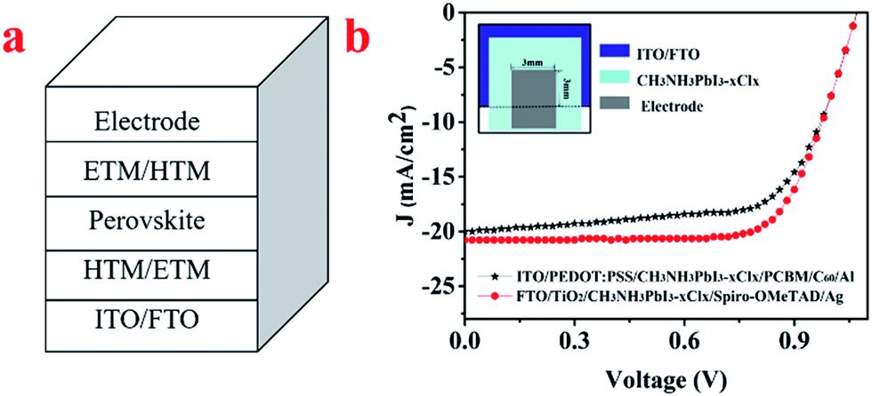 | ||
| Fig. 2 (a) The structure of the planar heterojunction perovskite solar cell. (b) The J–V characteristics of the devices under 100 mW cm−2 illumination of a calibrated simulated sunlight. (Inset: the device layout). | ||
By using LBIC mapping, the photoresponse of the real devices can be obtained. As an example, Fig. 3a shows the photoresponse result of the P–I–N device given in Fig. 2. The nonuniformity of the photoresponse is obvious. Similar results are also obtained for N–I–P devices though the distributions of photoresponse are different. One of the reasons for this nonuniformity might come from the thickness variation of perovskite film. As pointed by Liu et al.,17 the thickness variation of perovskite film fabricated from solution process is large. Generally, the too thin film is not so sufficient to absorb sunlight, while the too thick film would result in less carrier collection because the carrier diffusion length is shorter than the film thickness. However, a suitable film thickness does not always correspond to high photoresponse as it is the result of sequential processes of light absorb, charge separation, carrier transportation, and carrier collection. From this point of view, LBIC is a more direct way than morphology characterization techniques (AFM/SEM) to present the photoresponse distribution of a real device. As it is shown in Fig. 3b, the SEM image indicates the perovskite film is quite smooth and uniform based on images from randomly chosen locations. Thus this discrepancy indicates the cell with uniform film morphology does not mean that the photoresponse is uniform. Guided by LBIC method, the better performance area of a real device can be located for further research.
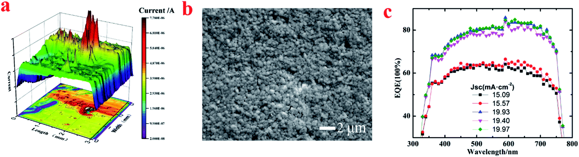 | ||
| Fig. 3 (a) Three-dimensional photoresponse shows the nonuniformity of PSC. (b) SEM image of the perovskite film prepared in the same batch shows the uniform morphology. (c) Apparent EQE action spectra and current integration of the same PSCs when focused the monochromatic light on different regions. | ||
Indeed, different apparent external quantum efficiency (EQE) values were obtained when focused monochromatic light was used for different device locations (ESI, Fig. S4†). As it is given in Fig. 3c, the integration of five apparent EQE curves presents two lower values of 15.09 mA cm−2, 15.57 mA cm−2 and three higher values of 19.93 mA cm−2, 19.40 mA cm−2, 19.97 mA cm−2. This result demonstrates that a higher efficiency can be achieved if a device only containing the better performance areas is fabricated.
The photoresponse of another device was mapped by LBIC technique and is shown in ESI (Fig. S1†). Compared with the left side, the photoresponse of the right side is much more uniform. Thus, the performance of device could be predictably improved as a result of removing the left side of the device with more defects. In accordance, the device performance is improved by preserving the area with better photoresponse. Although the FF decreased a little, the overall PCE increased from 10.88% to 11.58% due to the larger Jsc (from 19.44 mA cm−2 to 21.72 mA cm−2).
The LBIC was further used to trace the degradation of the perovskite solar cells with N–I–P structure. After fabrication, the device was transferred to the nitrogen-filled glove box without exposure to moisture. The J–V measurements were conducted in the glove box, showing a PCE of 15.49%, as given in Fig. 4. After 7 days' storage in the glove box, the overall performance decreases a little to 13.0% and then sharply drops to 1.38% after 28 days storage. The LBIC mapping for these three stages were conducted in the same glove box just after each J–V measurement. The LBIC mapping results are also shown in Fig. 4, being consistent with the J–V measurements. However, LBIC mapping shows that the uniformity of photoresponse becomes even worse after degradation. The degradation of the device have three possible sources, i.e. perovskite film itself, boundary of the perovskite crystalline, and the interfaces between perovskite film and the electrodes. However, the SEM morphology of the perovskite film shows negligible change after the same duration of storage for J–V and LBIC measurements, either with or without the HTL layer, as it is shown in Fig. 5 and 6. This unchanged morphology is confirmed by AFM measurement, as shown in Fig. 6. Thus the degradation is not mainly due to the morphology change of the film. And it also has high possibility that the degradation is not determined by the defects in the perovskite film or at the boundaries. Since the crystalline and boundary distributions are quite uniform on the whole device, as demonstrated in Fig. 5 and 6, the nonuniformity and uneven decrease of photoresponse from the LBIC mapping must be related to the top electrode. The nonuniformity of Fig. 3a and 4b is possible due to the nonuniform contact between the perovskite film and the top electrode. As the contact deterioration is further progressed after longtime storage, the performance of the device decreases and the uniformity of the photoresponse becomes worse.
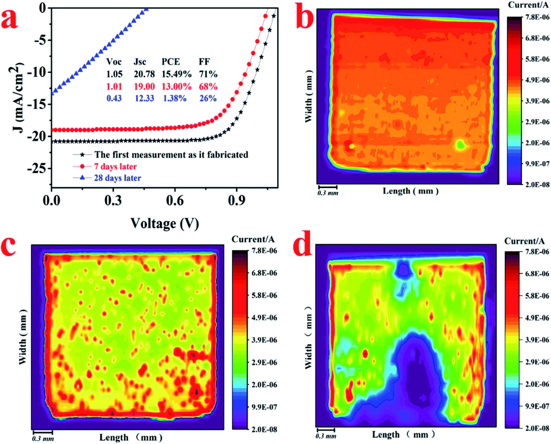 | ||
| Fig. 4 (a) J–V characteristics of a N–I–P structure device just after fabrication, after 7 days and 28 days storage in glove box, respectively. The LBIC results of photoresponse mapping of the same device after J–V measurements: (b) just after fabrication, (c) after 7 days storage in glove box, and (d) after 28 days storage in glove box. | ||
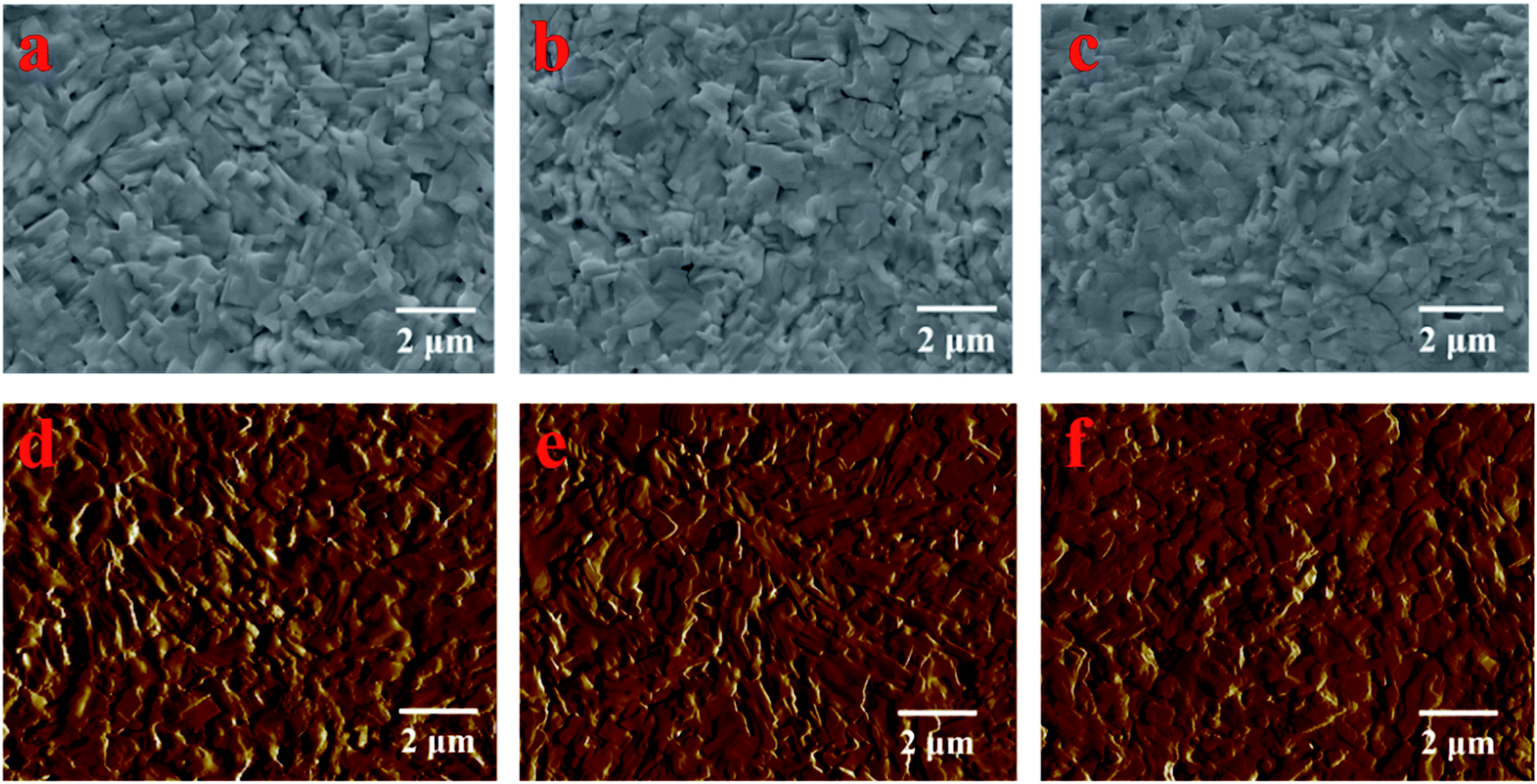 | ||
| Fig. 5 The SEM and AFM images for the perovskite film fabricated using the same procedure as for the real device. (a and d) Just after fabrication, (b and e) after 7 days storage in glove box, (c and f) after 28 days storage in glove box. | ||
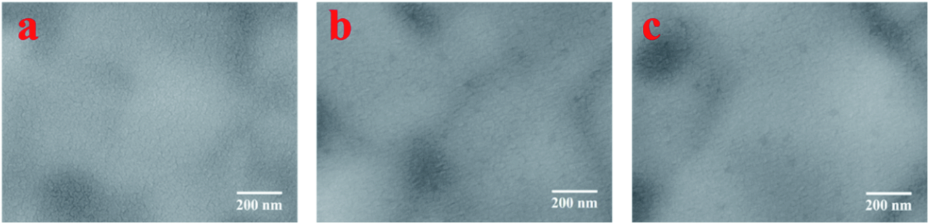 | ||
| Fig. 6 SEM images of the perovskite film from the same batch with HTL layer on top it. (a) Just after fabrication, (b) after 7 days storage in glove box, and (c) after 28 days storage in glove box. | ||
To confirm this conclusion, the optical images of the device with top electrode were obtained after the same period of storage in the glove box. As it is shown in Fig. 7, some small spots can be discerned under microscope. The reason for forming these spots is not clear at this stage. The possible reason is the trace moisture in the HTL layer (spiro-OMeTAD needs to be oxidized in the air during device fabrication, the additives in the spiro-OMeTAD are easy to absorb moisture) or in the glove box (O2/moisture: a few ppm) can degrade the HTL or react with top electrode. What's more, the illumination (AM 1.5 G) for J–V test can accelerate the degradation.
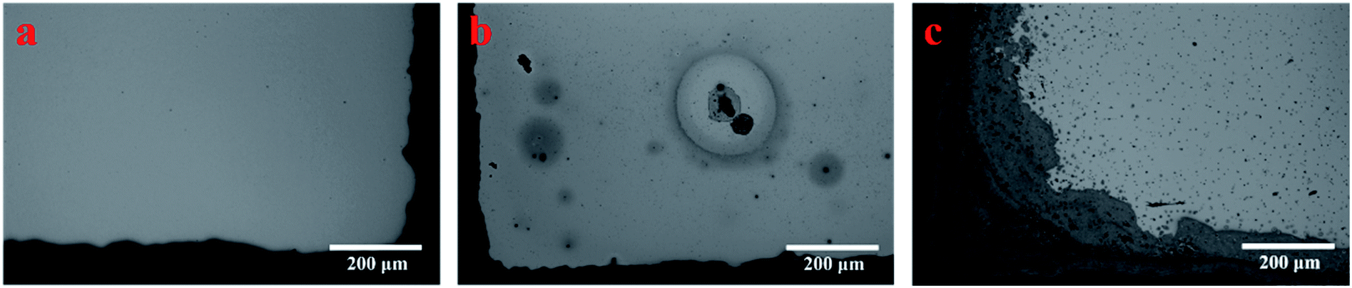 | ||
| Fig. 7 Optical images of the top electrode of an intact perovskite solar cell. (a) Just after fabrication, (b) after 7 days storage in glove box, and (c) after 28 days storage in glove box. | ||
Conclusion
LBIC is a powerful tool to characterize the photoresponse of real perovskite solar cells. The nonuniformity photoresponse of the real device becomes a sharp contrast to the uniform morphology of perovskite films. Moreover, the photoresponse distribution of perovskite solar cells monitored by LBIC technique shows a nonuniform degradation while the morphology keeps quite stable and uniform in the same duration. Though grain boundary defects may have some contributions, the deterioration of the interface between HTL/ETL and top electrode is more important for the degradation of devices kept in glove box.Conflicts of interest
There are no conflicts to declare.Acknowledgements
This work was supported by National Natural Science Foundation of China (Grant 11274256), Program for Innovation Team Building at Institutions of Higher Education in Chongqing (CXTDX201601011), Xinjiang Outstanding Young Scholars Foundation (QN2015YX004), Fundamental Research Funds for the Central Universities (XDJK2017A002).References
- A. Kojima, K. Teshima, Y. Shirai and T. Miyasaka, J. Am. Chem. Soc., 2009, 131, 6050–6051 CrossRef CAS PubMed
.
- J. H. Im, C. R. Lee, J. W. Lee, S. W. Park and N. G. Park, Nanoscale, 2011, 3, 4088–4093 RSC
- H. S. Kim, C. R. Lee, J. H. Im, K. B. Lee, T. Moehl, A. Marchioro, S. J. Moon, R. Humphry-Baker, J. H. Yum, J. E. Moser, M. Gratzel and N. G. Park, Sci. Rep., 2012, 2, 591 CrossRef PubMed
- L. Etgar, P. Gao, Z. Xue, Q. Peng, A. K. Chandiran, B. Liu, M. K. Nazeeruddin and M. Grätzel, J. Am. Chem. Soc., 2012, 134, 17396–17399 CrossRef CAS PubMed
- J. H. Noh, S. H. Im, J. H. Heo, T. N. Mandal and S. I. Seok, Nano Lett., 2013, 13, 1764–1769 CrossRef CAS PubMed
- N.-G. Park, J. Phys. Chem. Lett., 2013, 4, 2423–2429 CrossRef CAS
- J. Burschka, N. Pellet, S. J. Moon, R. Humphry-Baker, P. Gao, M. K. Nazeeruddin and M. Gratzel, Nature, 2013, 499, 316–319 CrossRef CAS PubMed
- M. A. Green, K. Emery, Y. Hishikawa, W. Warta and E. D. Dunlop, Prog. Photovoltaics, 2015, 23, 1–9 Search PubMed
- M. Saliba, T. Matsui, J. Y. Seo, K. Domanski, J. P. Correa-Baena, M. K. Nazeeruddin, S. M. Zakeeruddin, W. Tress, A. Abate, A. Hagfeldt and M. Gratzel, Energy Environ. Sci., 2016, 9, 1989–1997 CAS
- http://www.nrel.gov/ncpv/images/efficiencychart.jpg.
- X. Li, D. Bi, C. Yi, J. D. Decoppet, J. Luo, S. M. Zakeeruddin, A. Hagfeldt and M. Gratzel, Science, 2016, 353, 58–62 CrossRef CAS PubMed
- J.-P. Correa-Baena, A. Abate, M. Saliba, W. Tress, T. Jesper Jacobsson, M. Grätzel and A. Hagfeldt, Energy Environ. Sci., 2017, 10, 710–727 CAS
- H. Zhang, J. Cheng, F. Lin, H. He, J. Mao, K. S. Wong, A. K. Jen and W. C. Choy, ACS Nano, 2016, 10, 1503–1511 CrossRef CAS PubMed
- F. Si, F. Tang, H. Xue and R. Qi, J. Semicond., 2016, 37, 072003 CrossRef
- Q. Chen, H. Zhou, Z. Hong, S. Luo, H. S. Duan, H. H. Wang, Y. Liu, G. Li and Y. Yang, J. Am. Chem. Soc., 2014, 136, 622–625 CrossRef CAS PubMed
- P. Fan, D. Gu, G. X. Liang, J. T. Luo, J. L. Chen, Z. H. Zheng and D. P. Zhang, Sci. Rep., 2016, 6, 29910 CrossRef CAS PubMed
- M. Liu, M. B. Johnston and H. J. Snaith, Nature, 2013, 501, 395–398 CrossRef CAS PubMed
- H. Xie, X. Liu, L. Lyu, D. Niu, Q. Wang, J. Huang and Y. Gao, J. Phys. Chem. C, 2016, 120, 215–220 CAS
- T. Zhang, N. Guo, G. Li, X. Qian and Y. Zhao, Nano Energy, 2016, 26, 50–56 CrossRef CAS
- N. J. Jeon, J. H. Noh, Y. C. Kim, W. S. Yang, S. Ryu and S. I. Seok, Nat. Mater., 2014, 13, 897–903 CrossRef CAS PubMed
- D. Khatiwada, S. Venkatesan, N. Adhikari, A. Dubey, A. F. Mitul, L. Mohammad, A. Iefanova, S. B. Darling and Q. Qiao, J. Phys. Chem. C, 2015, 119, 25747–25753 CAS
- P. W. Liang, C. Y. Liao, C. C. Chueh, F. Zuo, S. T. Williams, X. K. Xin, J. Lin and A. K. Jen, Adv. Mater., 2014, 26, 3748–3754 CrossRef CAS PubMed
- D. Wei, T. Wang, J. Ji, M. Li, P. Cui, Y. Li, G. Li, J. M. Mbengue and D. Song, J. Mater. Chem. A, 2016, 4, 1991–1998 CAS
- R. K. Misra, L. Ciammaruchi, S. Aharon, D. Mogilyansky, L. Etgar, I. Visoly-Fisher and E. A. Katz, ChemSusChem, 2016, 9, 2572–2577 CrossRef CAS PubMed
- T. Xu, L. Chen, Z. Guo and T. Ma, Phys. Chem. Chem. Phys., 2016, 18, 27026–27050 RSC
- T. A. Berhe, W.-N. Su, C.-H. Chen, C.-J. Pan, J.-H. Cheng, H.-M. Chen, M.-C. Tsai, L.-Y. Chen, A. A. Dubale and B.-J. Hwang, Energy Environ. Sci., 2016, 9, 323–356 CAS
- T. Leijtens, G. E. Eperon, N. K. Noel, S. N. Habisreutinger, A. Petrozza and H. J. Snaith, Adv. Energy Mater., 2015, 5, 1500963 CrossRef
- W. Dimassi, L. Derbali, M. Bouaïcha, B. Bessaïs and H. Ezzaouia, Sol. Energy, 2011, 85, 350–355 CrossRef CAS
- N. Kwarikunda, E. E. van Dyk, F. J. Vorster, W. Okullo and M. K. Munji, Phys. B, 2014, 439, 122–125 CrossRef CAS
- R. Rösch, D. M. Tanenbaum, M. Jørgensen, M. Seeland, M. Bärenklau, M. Hermenau, E. Voroshazi, M. T. Lloyd, Y. Galagan, B. Zimmermann, U. Würfel, M. Hösel, H. F. Dam, S. A. Gevorgyan, S. Kudret, W. Maes, L. Lutsen, D. Vanderzande, R. Andriessen, G. Teran-Escobar, M. Lira-Cantu, A. Rivaton, G. Y. Uzunoğlu, D. Germack, B. Andreasen, M. V. Madsen, K. Norrman, H. Hoppe and F. C. Krebs, Energy Environ. Sci., 2012, 5, 6521 Search PubMed
- G. E. Eperon, D. Moerman and D. S. Ginger, ACS Nano, 2016, 10, 10258–10266 CrossRef CAS PubMed
- N. Kedem, T. M. Brenner, M. Kulbak, N. Schaefer, S. Levcenko, I. Levine, D. Abou-Ras, G. Hodes and D. Cahen, J. Phys. Chem. Lett., 2015, 6, 2469–2476 CrossRef CAS PubMed
- S. Mastroianni, F. D. Heinz, J. H. Im, W. Veurman, M. Padilla, M. C. Schubert, U. Wurfel, M. Gratzel, N. G. Park and A. Hinsch, Nanoscale, 2015, 7, 19653–19662 RSC
- Z. Song, A. Abate, S. C. Watthage, G. K. Liyanage, A. B. Phillips, U. Steiner, M. Graetzel and M. J. Heben, Adv. Energy Mater., 2016, 6, 1600846 CrossRef
- Z. Tang, S. Tanaka, S. Ito, S. Ikeda, K. Taguchi and T. Minemoto, Nano Energy, 2016, 21, 51–61 CrossRef CAS
- D. Yamashita, T. Handa, T. Ihara, H. Tahara, A. Shimazaki, A. Wakamiya and Y. Kanemitsu, J. Phys. Chem. Lett., 2016, 7, 3186–3191 CrossRef CAS PubMed
- Z. Song, J. Werner, N. Shrestha, F. Sahli, S. De Wolf, B. Niesen, S. C. Watthage, A. B. Phillips, C. Ballif, R. J. Ellingson and M. J. Heben, J. Phys. Chem. Lett., 2016, 7, 5114–5120 CrossRef CAS PubMed
- J. You, Z. Hong, Y. M. Yang, Q. Chen, M. Cai, T. B. Song, C. C. Chen, S. Lu, Y. Liu, H. Zhou and Y. Yang, ACS Nano, 2014, 8, 1674–1680 CrossRef CAS PubMed
- F. Wu, J. Liu, G. Wang, Q. Song and L. Zhu, Chemistry, 2016, 22, 16636–16641 CrossRef CAS PubMed
- G. Wang, D. Liu, J. Xiang, D. Zhou, K. Alameh, B. Ding and Q. Song, RSC Adv., 2016, 6, 43299–43303 RSC
- R. M. Geisthardt and J. R. Sites, IEEE J. Photovolt., 2014, 4, 1114–1118 CrossRef
Footnote |
| † Electronic supplementary information (ESI) available. See DOI: 10.1039/c7ra06423c |
| This journal is © The Royal Society of Chemistry 2017 |