
 Open Access Article
 This Open Access Article is licensed under a
 Creative Commons Attribution 3.0 Unported Licence
Synthesis of highly sensitive disordered porous SnO2 aerogel composite material by the chemical deposition method: synergistic effect of a layer of CuO thin film†
Tian-tian Lia,
Ren-rong Zhenga,
Hui Yu *a,
Ying Yang*ab,
Ting-ting Wanga and
Xiang-ting Donga
*a,
Ying Yang*ab,
Ting-ting Wanga and
Xiang-ting Donga
aSchool of Chemistry & Environmental Engineering, Changchun University of Science and Technology, Changchun 130022, P. R. China. E-mail: yh2001101@163.com; yangying0807@126.com; Fax: +86-431-85383815; Tel: +86-431-85583008
bKey Laboratory of Functional Inorganic Material Chemistry, Heilongjiang University, Ministry of Education, Harbin 150080, P. R. China
First published on 11th August 2017
Abstract
In this study, a new chemical deposition method was innovatively used to prepare disordered porous CuO/SnO2 aerogel composite material (CuO/SnO2-ACM). The CuO/SnO2-ACM was a p–p combined structure semiconductor, with a layer of CuO thin film formed on the surface of disordered porous SnO2 aerogel matrix material (SnO2-AMM). For the first time, the aerogel technology was used to prepare the porous tin dioxide material. The metal Cu was deposited on the surface of the SnO2-AMM to form the film. Finally, the sample was calcined, and a layer of CuO thin film was formed on the surface of the SnO2-AMM. Compared with the SnO2-AMM, the prepared CuO/SnO2-ACM showed enhanced sensitivity to NOx gas at the room temperature. When the NOx concentration was 100 ppm, the response reached 74%, and the response time was only 7.0 s. A detection limit to NOx gas of 1 ppm could be reached, with a response and response time of 15% and 26 s, respectively. In addition, excellent restorability and superior selectivity could be observed in the prepared sensor. The excellent gas sensing properties of the prepared CuO/SnO2-ACM can be attributed to the unique structure and synergistic effect of CuO thin film.
1. Introduction
There are abundant harmful gases in the environment, such as acetone, sulfur dioxide, carbon monoxide, nitrogen oxides and so on. Environmental pollution has become a very critical problem in recent years.1 In order to control this situation, most of the semiconductor gas sensors are made from MOS (metal oxide semiconductor), which are widely used to detect, monitor, control the toxic and harmful gases. They show a good application prospect in environmental science.2–9 As a broad-spectrum semiconductor, SnO2 has been extensively studied as a gas sensing material.10 Compared with other semiconductor gas sensitive materials, SnO2 has many advantages, such as simple manufacture, fast response and recovery times, a high sensitivity to oxidation gases, etc.11–13 Different methods can be used to prepare various structural SnO2 materials, including surface modification of materials and doping of materials to improve the their performance for gas sensing.14 The sensing properties of a gas sensor are greatly influenced by the microstructures, grain size, morphologies, and temperature.15,16 SnO2 materials have been prepared with different structures,17 such as nanotubes,18 nanorods,19 nanosheets,20 nanofibers,21 hollow spheres,22 hierarchical flowerlike nanostructures,23 hollow porous microcubes, etc.24–28 With the deepening of the research, it is found that the gas sensing properties of the SnO2-based composite materials are much higher than those of pure SnO2. Mishra et al.9 described Cu-doped SnO2 nanoparticles, which were synthesized by a co-precipitation method, and were then investigated as a formaldehyde sensing material. The 1.5 wt% Cu-doped SnO2 showed a selective high response (∼80%) to 50 ppm concentration of formaldehyde at 200 °C. Qin et al.15 prepared Nd-doped SnO2 nanorods by a substrate-free hydrothermal route of using sodium stannate and sodium hydroxide at 210 °C. The Nd-doped SnO2 nanorods with an optimized Nd doping level of 3.0 wt% exhibited an excellent sensing response toward alcohol at 260 °C. Li et al.2 demonstrated Cu2+/Au co-doped SnO2 nanofibers by electrospinning method, which were used to detect acetylene (C2H2) at 160 °C.CuO was reported to have outstanding promotive action.29 CuO/SnO2 heterostructures revealed an extraordinary performance in sensors.30,31 The p-type CuO and n-type SnO2 form a p–n junction with a depletion zone. Some studies reported a highly sensitive CuO–SnO2 composite nano-fibers for H2S detection.32,33 Considerable efforts have been focused on fabricating of the one-dimensional nano materials via thermal oxidation, thermal evaporation, hydrothermal process and electro-spinning.30,34 Li et al. synthesized Cu-doped SnO2 nano fibers via electro-spinning, and the rapid response to ethanol was reported.35 Shao et al.36 reported p-CuO (particle)/n-SnO2 (nanowire) heterostructures devices and their application as H2S sensors. CuO/SnO2 films were one of the most promising for detecting H2S.30,37,38 The Cu element was dispersed either in the form of islands or as a continuous layer on the surface of the SnO2 film, which showed a reasonably strong sensor response to H2S.34 Toan et al. reported the H2S gas sensors using SnO2 thin films sensitized with CuO islands.39 Choi et al. proposed that CuO loaded SnO2 hollow spheres showed almost negligible humidity dependence of sensor signal even under highly humid (RH of 80%) atmosphere as well as ultrahigh response and selectivity to sub-ppm H2S.40 Multilayered SnO2–CuO thin films were also fabricated for highly sensitive H2S sensing.41
Porous materials are used in gas sensitive field which can be attributed to their effective surface area and porosity.42 The porous structures can increase the specific surface areas of the materials, effectively. The large specific surface area means that the atoms are located on the surface, and participate in surface reactions. The porous materials can provide the more active sites, improve the surface adsorption capacity to gases, and make the gases spread into the prepared material, which finally enhance the gas-sensing properties of samples.43 Therefore, the preparation of porous SnO2-based composite materials is an obvious trend. It has been reported that the mesoporous structure can provide high surface area and well-defined porous architecture for high gas response and rapid gas responding kinetics.44 A series of porous SnO2 semiconductor materials were widely used for gas sensors.45 Guo et al.46 have also investigated the gas sensing performances of mesoporous SnO2 towards toxic gases with a different reducing ability. The ordered periodical structures and large specific surface area allow for improved performances.47–51 The ordered 2D mesoporous SnO2 structures with high crystallinity and large surface area have been successfully prepared by using nanocasting method for detecting a variety of gases.52 Compared with the ordered porous materials, the disordered porous SnO2 aerogel composite material is very meaningful. The disordered porous SnO2 aerogel has the higher porosity, which has the higher gas-sensing properties. Until now, it is without reported about the disordered porous SnO2 aerogel.
In this study, the disordered porous CuO/SnO2 aerogel composite materials with excellent gas sensing properties were successfully prepared by the chemical deposition method. The study was quite different from the past reported articles in preparation and gas sensing. First, the aerogel technology was used to prepare the porous tin dioxide material. Second, the metal Cu was deposited on the surface of the prepared porous SnO2 material to form the film, which was calcined, and a layer of CuO thin film was formed on the surface of the prepared porous SnO2 material. The structure of the prepared material was characterized by X-ray diffraction (XRD), scanning election microscope (SEM), transmission electron microscopy (TEM), N2 adsorption–desorption method and energy dispersive X-ray spectrometer (EDS). The gas sensing properties of CuO/SnO2-ACM to NOx gas were investigated. The synthesized CuO/SnO2-ACM was provided with excellent gas sensing properties, high sensitivity, good stability, fast response time.
2. Experimental section
All chemicals used in this work were of analytical grade, and without further purification. Tin(II) chloride dihydrate (SnCl2·2H2O, A.R.) was purchased from Xilong Chemical Research Institute in China. Tetraethyl silicate (TEOS, A.R.), n-hexane (A.R.) and sodium hydroxide (NaOH, A.R.) were purchased from Beijing Chemical Works Research Institute in China. Potassium sodium tartrate tetrahydrate (C4H4O6KNa·4H2O, A.R.) was purchased from Tianjin Guangfu Technology Development Co., Ltd in China. Formaldehyde solution (HCHO, A.R.) was purchased from Tianjin Fuchen Chemical Reagents Factory in China. Ethylene diamine tetraacetic acid disodium (EDTA-2Na, A.R.) was purchased from Shenyang Reagent Factory in China. Copper(II) sulfate pentahydrate (CuSO4·5H2O, A.R.) was purchased from Sinopharm Chemical Reagent Co., Ltd in China. Ethanol and deionized water were used for all process of washing and dissolution.2.1. Synthesis
2.2. Characterizations
The crystallographic structures of the prepared CuO/SnO2-ACM was determined using X-ray diffraction (XRD, Siemens D5005, with high-intensity Cu-Kα radiation with a wavelength of 1.5418 Å). The morphology and composition of the prepared materials were investigated by scanning election microscope (SEM, JEOL JSM-5600L) with an energy dispersive X-ray spectrometer (EDS). The microstructures of the prepared materials were investigated by transmission electron microscopy (TEM, JEOL 2010 TEM instrument). Physical adsorption of nitrogen was performed on a Micromeritics ASAP2010M volumetric adsorption analyzer at 77 K. The CuO/SnO2-ACM was degassed in vacuum at 573 K for 12 h before measurement. Surface area was calculated based on the BET model, while pore size was computed using the BJH method.2.3. Gas sensing measurements
An interdigitated Au electrode (7 × 5 × 0.25 mm) was selected for gas sensing detection, and the finger spacing was 20 μm. The prepared CuO/SnO2-ACM was dispersed in ethanol to form a suspension. Then, the suspension was coated onto the electrode. It was dried at 60 °C for 1 h to obtain a thin film gas sensor.The responses of the prepared gas sensor to the different concentrations NOx gas were performed. The sensor was placed in a static flow system, which has only one inlet and one outlet. The test chamber needed to be pumped for 2 min to let the sample room full of air, and obtain the stable absorption film. A syringe was used to inject gas into the sample room, and observed the change of resistance. The response is signed as S, which is calculated according to reported equation (eqn (1)):53,54
| S (%) = [(Rg − Ra/Ra)] × 100 | (1) |
3. Results and discussion
3.1. Structural characterizations
Fig. 1 showed the XRD patterns of the prepared SnO2-AMM and CuO/SnO2-ACM. In Fig. 1(a), the diffraction peaks at 26.8°, 34.3°, 37.9°, 52.1°, 54.7°, 62.9°, 64.3°, 71.4° and 78.7° could be assigned to (110), (101), (200), (211), (220), (310), (301), (202) and (321) planes of SnO2 with tetragonal rutile structure (PDF# 41-1445). In Fig. 1(b), the diffraction peaks at 32.5°, 35.4° and 38.9° could be assigned to (110), (002) and (200) planes of CuO with monoclinic system structure, which was consistent with the data format of the standard data file PDF# 48-1548. All of the diffraction patterns were attributed to the characteristic peaks of CuO and SnO2, and no other diffraction peak was observed. It showed that the CuO has been successfully coated on the surface of the SnO2-AMM. It could be proved that the disordered porous CuO/SnO2 aerogel composite material could be obtained by the chemical deposition method. From the Fig. 1, the peaks of the SnO2 and CuO were broadened. It could be attributed to the lower crystallization degrees of the sample, which was the defect of sol–gel method, and the introduced CuO further reduced the crystallization degrees.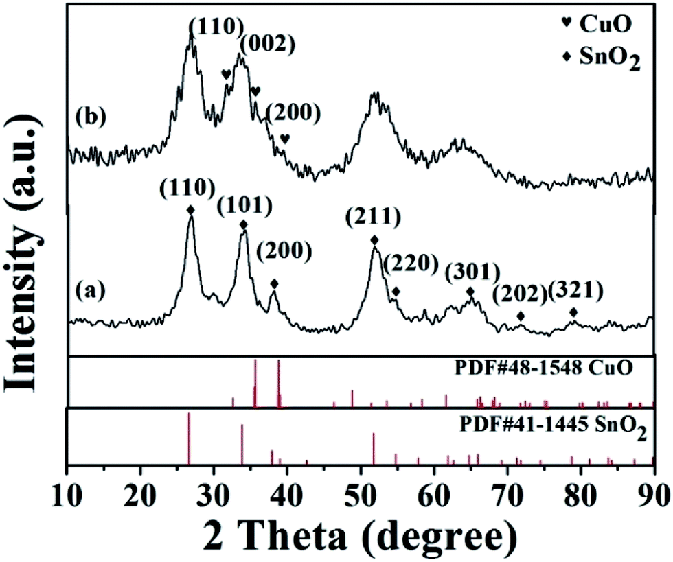 | ||
| Fig. 1 XRD patterns of (a) SnO2-AMM, and (b) CuO/SnO2-ACM. | ||
The morphology and microstructure of the prepared materials were determined using SEM. Fig. 2(a) and (b) showed the SEM images of the prepared CuO/SnO2-ACM sample. Fig. 2(a) indicated that the morphology of the CuO/SnO2-ACM was cluster like loosened structure in the lower magnification. The clusters were consisted of irregular sphere particles, and the diameters of those sphere particles were ranges from 100–200 nm in the Fig. 2(b). Fig. 2(c) showed the SEM images of the prepared Cu/SnO2 sample, which showed also the cluster like structure. The clusters were consisted of irregular sphere particles, which showed the serious agglomeration. In order to research the microstructure of the prepared materials, the typical TEM images were collected, which was taken with the beam direction parallel to the pores, the result were shown in Fig. 2(d). It could be clearly seen that its surfaces distributed the disordered loosened porous, which was easier to adsorb gas. The TEM image of Cu/SnO2 sample was showed in Fig. 2(e). It could be clearly seen that its surfaces distributed the disordered porous structure, whose poriness was lower than CuO/SnO2-ACM sample. The composition of the CuO/SnO2-ACM was determined from the EDS spectrum in the Fig. 2(f). The signals of Si and C were introduced from the silicon slice and conducting resin, which were used in the test procedure. The prepared CuO/SnO2-ACM was composed of Cu, Sn and O species. From EDS analysis results, the atomic percentages of Sn, O and Cu were 55.8 wt%, 40.3 wt% and 3.9 wt%, respectively.
 | ||
| Fig. 2 (a) and (b) SEM images of the CuO/SnO2-ACM. (c) SEM images of the Cu/SnO2. (d) and (e) TEM image of the CuO/SnO2-ACM and Cu/SnO2. (f) EDS spectrum of the CuO/SnO2-ACM. | ||
Fig. 3 showed the low temperature nitrogen adsorption–desorption isotherms of the prepared SnO2-AMM (Fig. 3(a)) and CuO/SnO2-ACM (Fig. 3(b)). The isotherms belonged to the typical irreversible IV type isotherms with H1 hysteresis loop, which was the feature of the cylindrical pore. From Fig. 3, the adsorbing capacity gently increased at low pressure, it could be due to which the N2 molecules were absorbed on the inner surface of the pores in the form of single layer to multi-layer. In the high pressure, capillary condensations were happened, the isotherms rose rapidly, and the lag phenomenon was observed. The steep adsorption hysteresis associated with the narrow pore size distribution (the illustrations of the Fig. 3), which indicated that the pores of the samples were homogeneous. The specific surface area and pore size distribution were calculated by BET method and BJH model, respectively. The specific surface area, the most probable pore diameter, pore volume of the SnO2-AMM and CuO/SnO2-ACM were 74.935 and 66.627 m2 g−1, 1.80 and 1.60 nm, 0.228 and 0.217 cm3 g−1, respectively. The three values of the CuO/SnO2-ACM sample were smaller than the SnO2-AMM. It illustrated that the CuO was coated on the surface of the SnO2-AMM, and formed a layer of CuO thin film on the surface of SnO2-AMM.
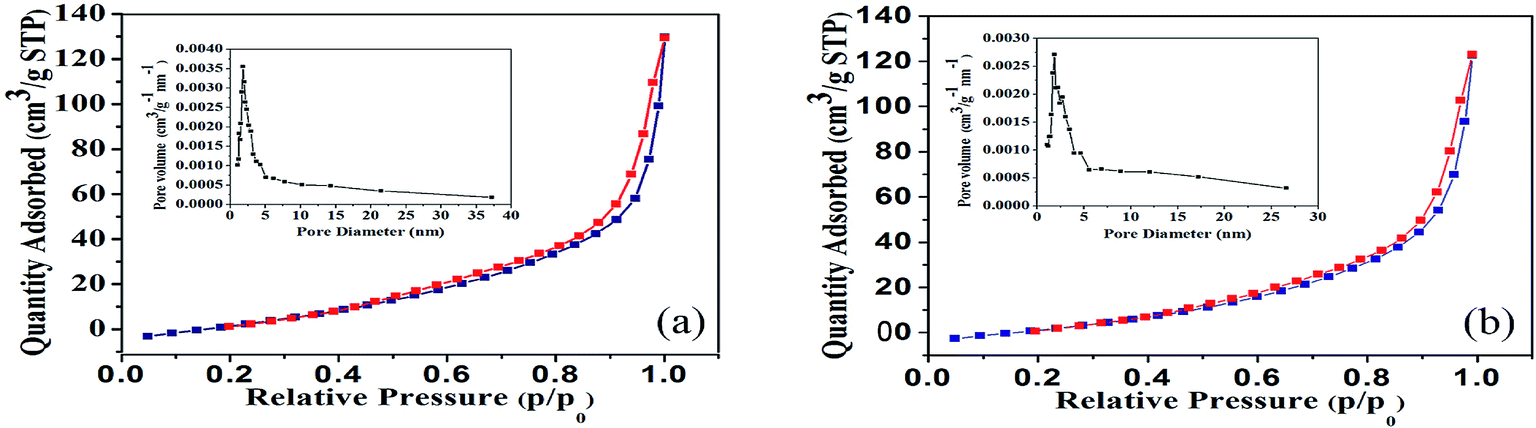 | ||
| Fig. 3 Nitrogen adsorption–desorption isotherm and pore diameter distribution of (a) SnO2-AMM, and (b) CuO/SnO2-ACM. | ||
3.2. Gas sensing properties
At room temperature, the gas sensing properties of the prepared materials to nitrogen oxides (NOx) were tested by thin film sensors, which were prepared using the SnO2-AMM and CuO/SnO2-ACM. Fig. 4(a) and (c) were the response–recovery curves of the SnO2-AMM and CuO/SnO2-ACM gas sensor during cyclic exposure in different concentrations NOx, respectively. The resistance sharply decreased, and gradually reached the minimum resistance in a very short period of time when NOx gas was injected into the sample room. After the gas was withdrawn, the resistance was quickly recovered to the previous value. It was the typical of the p-type semiconductor, and the CuO/SnO2-ACM was a p–p combined structure semiconductor. From the Fig. 4(a) and (c), the prepared thin film sensor had a better response to the NOx gas, and the sensor could be repeated without a noticeable properties decrease. It could be seen that the detection limit of the CuO/SnO2-ACM sensor (1 ppm) was lower than SnO2-AMM sensor (5 ppm). Its recovery performance was also much better than SnO2-AMM sensor. | ||
| Fig. 4 (a) and (c) The response–recovery curves of SnO2-AMM and CuO/SnO2-ACM gas sensor during cyclic exposure in different concentrations NOx. (b and d) Response and response time curve of SnO2-AMM and CuO/SnO2-ACM gas sensor in the different concentration NOx at the room temperature. (e) The gas sensing performance bar graphs of SnO2-AMM and CuO/SnO2-ACM gas sensor. (f) The gas response bar graphs of CuO/SnO2-ACM sensor in different gases (NOx, NH3, H2, O2, N2). | ||
Fig. 4(b) and (d) showed the response and response time curve of the SnO2-AMM and CuO/SnO2-ACM sensor towards the different concentration NOx at the room temperature, respectively. With the NOx concentration decrease, the responses were also reducing. With the NOx concentration increase, the response time decreased. The concrete data was shown in ESI Table S1.† In Fig. 4(b), the response reached a maximum value of 54%, and the response time was 19.5 s when the NOx gas concentration was 100 ppm. From 100 to 5 ppm NOx concentration, the response time of the SnO2-AMM sensor ranged from 19.5 to 26 s. The minimum detection limit of the SnO2-AMM sensor was 5 ppm, whose response and response time were 40% and 26 s, respectively. In Fig. 4(d), the response reached a maximum value of 74%, and the response time was only 7 s when the NOx gas concentration was 100 ppm. From 100 to 1 ppm NOx concentration, the response time of the CuO/SnO2-ACM sensor ranged from 7 to 26 s. The minimum detection limit of the CuO/SnO2-ACM sensor was 1 ppm, whose response and response time were 15% and 26 s, respectively. There was a sudden jump in response time when the NOx concentration decreases from 10 to 5 and then 3 ppm. In porous materials, the gas adsorption capacity is connected with the gas partial pressures. At low partial pressures, the adsorption is mainly monolayer adsorption, the capillary condensation cannot occur. The adsorption is multilayer adsorption when the relative pressure increases to the capillary condensation occurring, and adsorptive quantity sharply increases (as Fig. 3). In this study, the gas adsorption capacity sharply declined when the NOx gas concentration reduced under 10 ppm, which led to response and response time a sudden jump. The gas sensing performance comparison bar chart of the SnO2-AMM and CuO/SnO2-ACM sensor was shown in Fig. 4(e). It proved that the response and response time of the CuO/SnO2-ACM sensor were far superior to the SnO2-AMM sensor.
The gas selectivity is a very important factor for the application of the sensor. Fig. 4(f) showed the gas response bar graphs of the CuO/SnO2-ACM sensor in different gases (NOx, NH3, H2, O2, N2). The concrete data could be found in ESI Table S2.† It showed that the response of the CuO/SnO2-ACM thin film sensor to NOx was much higher than the other gases at the same gas concentration. The response reached a maximum value of 74% when the NOx gas concentration was 100 ppm. For the same NH3 gas concentration, the maximum response was only 54%. It all know, NH3 is a reductive gas, NO2 is an oxidizing gas, and their detection effects have the much bigger difference, the similar result has been obtained in the past research.55 The responses of other gases were closer to 0%. It proved that the CuO/SnO2-ACM sensor had the better selectivity to NOx.
3.3. Sensing mechanism
As Fig. 4(c), the resistance of the sample sharply decreases when NOx gas is injected into the sample room, which is the typical characteristic of p-type semiconductors. Therefore, the prepared CuO/SnO2-ACM is a p–p type metal-oxide semiconductor. Fig. 5 is the microstructure schematic diagram and corresponding sensing mechanism of the CuO/SnO2-ACM sensor. From Fig. 5, the oxygen (O2) will be chemisorbed, and capture some electrons from the conduction band of SnO2 material when the thin film sensor is exposed in the air ambient. It can form an electron depletion layer on the surface of the CuO/SnO2-ACM sensor, the O2−, O− and O2− species will be created, and they form a follow chemical equilibrium with each other:| O2 ↔ O−2 ↔ O− ↔ O2− | (2) |
 | ||
| Fig. 5 The microstructure schematic diagram and corresponding sensing mechanism of CuO/SnO2-ACM sensor. | ||
This is the reason why the resistance tends to be stable.56,57 This system has the better catalytic activity in the CuO/SnO2-ACM sensor. The NOx gas molecules are oxidized when the thin film sensor is exposed into the oxidation type gas (NOx), which leads that the oxygen ions on the sensor surface are continuously reduced. At the same time, the exhausted electrons are fed back into the conductance band of the CuO/SnO2-ACM, which leads to the decrease of the resistance, and produce of the electrical signals. This reaction between adsorbed oxygen and NOx gas can be described as the following eqn (3) and (4):
| NO2 + e− → NO−2/NO + e− → NO− | (3) |
| NO2 + O− → NO−3/NO + O− → NO−2 | (4) |
Detailed process can be known through the schematic diagram in the Fig. 5. After filling in the NOx gas, the resistance of the CuO/SnO2-ACM sensor decreases sharply (Fig. 5). The thin film sensor is exposed to the air again when the NOx gas is drowned out, and the resistance is quickly restored to its original value.54,58–60 The above is the principle of the gas sensing performance test.
It is well known that the gas-sensing performance of the sensor is related to the structure of the gas sensing material. The larger specific surface area provides the more gas adsorption sites, the faster response to the gas, the better the gas sensing performance. In this study, the porous structures can effectively increase the specific surface area of the material. Material with high porosity structure can make the gas reach the gas sensitive material effectively and quickly, and a series of reactions occur effectively and quickly. It also can improve the response, response and recovery time of the sensing material.
In this study, the response towards NOx is largely promoted by the CuO film. The CuO/SnO2-ACM is p–p combined structure semiconductor gas sensor. It bases on the compensation-feedback principle of two different sensors. In Fig. 5, this particular type of semiconductor sensor can effectively improve the response of the sensor and the selectivity toward gas, which can be due to p–p transition layer formation. Cu2+ (0.073 nm) ion radius is close to Sn4+ (0.069 nm), which makes the nodes replace happen, the grain size decrease, and it does not cause serious lattice mismatch. It is well known that the smaller the grain size leads to the more active sites on the surface, which increases the response activity. In addition, Cu2+ ions occupy the position of Sn4+ ion, provide electrons, and the more free electrons participate in the gain and loss electronic of the reaction. It can produce the more oxygen adsorption centers, and increase the number of adsorbed oxygen. Therefore, the porous CuO/SnO2-ACM has the higher response. The prepared CuO/SnO2-ACM will have a great development space in the gas sensor field, and there is a great research value.
4. Conclusions
This study presents a method to prepare the disordered porous CuO/SnO2 aerogel composite material, which is the chemical deposition method. The prepared CuO/SnO2-ACM is a p–p combined structure semiconductor, a layer of CuO thin film is formed on the surface of the SnO2-AMM. The synthesized CuO/SnO2-ACM appears excellent gas sensing properties, the higher and faster response. At room temperature, its response is up reached to 74%, and the response time is only 7 s in 100 ppm NOx gas. The detection limit to NOx gas is only 1 ppm, and the corresponding response and response time are 15% and 26 s, respectively. The prepared CuO/SnO2-ACM gas-sensing material has an admirable detection performance and the better selectivity to NOx gas. The porous gas sensitive materials with high porosity has excellent gas sensing properties, and has the much better development prospects in the gas sensors field.Conflicts of interest
There are no conflicts to declare.Acknowledgements
We gratefully acknowledge the support of the work by the National Natural Science Foundation of China (Grant no. 51572034), the National Natural Science Foundation of China (Grant no. 21601018) and the National Natural Science Foundation of Changchun University of Science and technology (No. XQNJJ-2015-07).References
- R. J. Lu, W. Zhou, K. Y. Shi, Y. Yang, L. Wang, K. Pan, C. G. Tian, Z. Y. Rena and H. G. Fu, Nanoscale, 2013, 5, 8569–8576 RSC.
- Z. Y. Li, X. G. Wang and T. Lin, J. Mater. Chem. A, 2014, 2, 13655–13660 CAS.
- S. F. Shao, H. Y. Wu, F. Jiang, S. M. Wang, T. Wu, Y. T. Lei, R. Koehn and W. F. Rao, RSC Adv., 2016, 6, 22878–22888 RSC.
- S. F. Shao, H. Y. Wu, S. M. Wang, Q. L. Hong, R. Koehn, T. Wu and W. F. Rao, J. Mater. Chem. C, 2015, 3, 10819–10829 RSC.
- H. Nguyen and S. A. El-Safty, J. Phys. Chem. C, 2011, 115, 8466–8474 CAS.
- S. Li, T. Liu, Y. Zhang, W. Zeng, F. Pan and X. Peng, Mater. Lett., 2015, 143, 12–15 CrossRef CAS.
- W. Q. Li, S. Y. Ma, J. Luo, Y. Z. Mao, L. Cheng, D. J. Gengzang, X. L. Xu and S. H. Yan, Mater. Lett., 2014, 132, 338–341 CrossRef CAS.
- I. Lee, S.-J. Choi, K.-M. Park, S. S. Lee, S. Choi, I.-D. Kim and C. O. Park, Sens. Actuators, B, 2014, 197, 300–307 CrossRef CAS.
- R. K. Mishra, A. Kushwaha and P. P. Sahay, RSC Adv., 2014, 4, 3904–3912 RSC.
- Q. Yan, S. Tao and H. Toghiani, Talanta, 2009, 77, 953–961 CrossRef CAS PubMed.
- K. P. Gattu, K. Ghule, A. A. Kashale, V. B. Patil, D. M. Phase, R. S. Mane, S. H. Han, R. Sharrna and A. V. Ghule, RSC Adv., 2015, 5, 72849–72856 RSC.
- S. F. Bamsaoud, S. B. Rane, R. N. Karekar and R. C. Aiyer, Sens. Actuators B, 2011, 153(2), 382–391 CrossRef CAS.
- Z. Lou, L. Wang, R. Wang, T. Fei and T. Zhang, Solid-State Electron., 2012, 76, 91–94 CrossRef CAS.
- M. X. Chen, C. C. Zhang, L. Z. Li, Y. Liu, X. C. Li, X. Y. Xu, F. L. Xia, W. Wang and J. P. Gao, ACS Appl. Mater. Interfaces, 2013, 5(24), 13333–13339 CAS.
- G. Qin, F. Gao, Q. Jiang, Y. Li, Y. Liu, L. Luo, K. Zhao and H. Zhao, Phys. Chem. Chem. Phys., 2016, 18, 5537–5549 RSC.
- Z. P. Li, Q. Q. Zhao, W. L. Fan and J. H. Zhan, Nanoscale, 2011, 3, 1646–1652 RSC.
- A. Katoch, J.-H. Kim, Y. J. Kwon, H. W. Kim and S. S. Kim, ACS Appl. Mater. Interfaces, 2015, 7(21), 11351–11358 CAS.
- P. Sun, L. You, Y. F. Sun, N. K. Chen, X. B. Li, H. B. Sun, J. Ma and G. Y. Lu, CrystEngComm, 2012, 14, 1701–1708 RSC.
- S. Wang, J. Yang, H. Zhang, Y. Wang, X. Gao, L. Wang and Z. Zhu, Sens. Actuators, B, 2015, 207(A), 83–89 CrossRef CAS.
- T. Tao, L. He, J. Li and Y. Zhang, Mater. Lett., 2015, 138, 45–47 CrossRef CAS.
- L. Wang, J. Deng, Z. Lou and T. Zhang, J. Mater. Chem. A, 2014, 2, 10022–10028 CAS.
- Y. H. Cho, X. Liang, Y. C. Kang and J.-H. Lee, Sens. Actuators, B, 2015, 207(A), 330–337 CrossRef CAS.
- L. L. Wang, T. Fei, Z. Lou and T. Zhang, ACS Appl. Mater. Interfaces, 2011, 3(12), 4689–4694 CAS.
- J. R. Huang, L. Y. Wang, C. P. Gu and J.-J. Shim, Mater. Lett., 2014, 136, 371–374 CrossRef CAS.
- J. R. Huang, L. Y. Wang, C. P. Gu, M. H. Zhai and J. H. Liu, CrystEngComm, 2013, 15, 7515–7521 RSC.
- H. J. Song, X. H. Jia, H. Qi, X. F. Yang, H. Tang and C. Y. Min, J. Mater. Chem., 2012, 22, 3508–3516 RSC.
- G. X. Ma, R. J. Zou, L. Jiang, Z. Y. Zhang, Y. F. Xue, L. Yu, G. S. Song, W. Y. Li and J. Q. Hu, CrystEngComm, 2012, 14, 2172–2179 RSC.
- Q. Z. Jiao, M. Fu, C. You, Y. Zhao and H. S. Li, Inorg. Chem., 2012, 51, 11513–11520 CrossRef CAS PubMed.
- J. H. Jeun and S. H. Hong, Sens. Actuators, B, 2010, 151, 1–7 CrossRef CAS.
- I. S. Hwang, J. K. Choi, S. J. Kim, K. Y. Dong, J. H. Kwon, B. K. Ju and J. H. Lee, Sens. Actuators, B, 2009, 142, 105–110 CrossRef CAS.
- X. Y. Xue, L. Xing, Y. Chen, S. Shi, Y. Wang and T. Wang, J. Phys. Chem. C, 2008, 112, 12157–12160 CAS.
- S. Choi, A. Katoch, J. Zhang and S. S. Kim, Sens. Actuators, B, 2013, 176, 585–591 CrossRef CAS.
- S. W. Choi, J. Zhang, K. Akash and S. S. Kim, Sens. Actuators, B, 2012, 169, 54–60 CrossRef CAS.
- V. Kumara, S. Sen, K. P. Muthe, N. K. Gaur, S. K. Gupta and J. V. Yakhmi, Sens. Actuators, B, 2009, 138, 587–590 CrossRef.
- L. Liu, T. Zhang, L. Y. Wang and S. C. Li, Mater. Lett., 2009, 63, 2041–2043 CrossRef CAS.
- F. Shao, M. W. G. Hoffmann, J. D. Prades, R. Zamani, J. Arbiol, J. R. Morante, E. Varechkina, M. Rumyantseva, A. Gaskov, I. Giebelhaus, T. Fischer, S. Mathur and F. Hernández-Ramírez, Sens. Actuators, B, 2013, 181, 130–135 CrossRef CAS.
- M. Verma, A. Chowdhuri, K. Sreenivas and V. Gupta, Thin Solid Films, 2010, 518, E181–E182 CrossRef.
- Z. Xu, G. Duan, Y. Li, G. Liu, H. Zhang, Z. Dai and W. Cai, Chem.–Eur. J., 2014, 20, 6040–6046 CrossRef CAS PubMed.
- N. V. Toan, N. V. Chien, N. V. Duy, D. D. Vuong, N. H. Lam, N. D. Hoa, N. V. Hieu and N. D. Chien, Appl. Surf. Sci., 2015, 324, 280–285 CrossRef.
- K. I. Choi, H. J. Kim, Y. C. Kang and J. H. Lee, Sens. Actuators, B, 2014, 194, 371–376 CrossRef CAS.
- M. K. Verma and V. Gupta, Sens. Actuators, B, 2012, 166–167, 378–385 CrossRef CAS.
- P.-P. Zhang, H. Zhang and X.-H. Sun, Nanoscale, 2016, 8, 1430–1436 RSC.
- M. A. Andio, P. N. Browning, P. A. Morris and S. A. Akbar, Sens. Actuators, B, 2012, 165, 13–18 CrossRef CAS.
- J. H. Lee, Sens. Actuators, B, 2009, 140, 319–336 CrossRef CAS.
- X. X. Xu, J. Zhuang and X. Wang, J. Am. Chem. Soc., 2008, 130, 12527–12535 CrossRef CAS PubMed.
- W. Guo, X. C. Duan, Y. Shen, K. Z. Qi, C. Y. Wei and W. J. Zheng, Phys. Chem. Chem. Phys., 2013, 15, 11221–11225 RSC.
- Y. Ren, Z. Ma and P.G. Bruce, Chem. Soc. Rev., 2012, 41, 4909–4927 RSC.
- W. Li and D. Y. Zhao, Chem. Commun., 2013, 49, 943–946 RSC.
- Y. Teng, L. X. Song, A. Ponchel, Z. K. Yang and J. Xia, Adv. Mater., 2014, 26, 6238–6243 CrossRef CAS PubMed.
- Y. Teng, L. X. Song, A. Ponchel, E. Monflier, Z. C. Shao, J. Xia and Z. K. Yang, RSC Adv., 2014, 4, 26847–26854 RSC.
- A. Lannoy, R. Bleta, C. Machut, E. Monflier and A. Ponchel, RSC Adv., 2014, 4, 40061–40070 RSC.
- J. Zhao, W. N. Wang, Y. P. Liu, J. M. Ma, X. W. Li, Y. Du and G. Y. Lu, Sens. Actuators, B, 2011, 160, 604–608 CrossRef CAS.
- T. Becker, S. Ahlers, C. Braunmuhl, G. Muller and O. Keisewetter, Sens. Actuators, B, 2001, 77, 55–58 CrossRef CAS.
- Y. Yang, C. G. Tian, J. C. Wang, L. Sun, K. Y. Shi, W. Zhou and H. G. Fu, Nanoscale, 2014, 6, 7369–7378 RSC.
- J. Zhang, S. Wang, Y. Wang, M. Xu, H. Xia, S. Zhang and S. Wu, Sens. Actuators, B, 2009, 139, 411–417 CrossRef CAS.
- Y. Yang, L. Sun, X. T. Dong, H. Yu, T. T. Wang, J. X. Wang, R. H. Wang, W. S. Yu and G. X. Liu, RSC Adv., 2016, 6, 37085–37092 RSC.
- S. J. Choi, S. Chattopadhyay, J. J. Kim, S.-J. Kim, H. L. Tuller, G. C. Rutledge and I.-D. Kim, Nanoscale, 2016, 8(17), 9159–9166 RSC.
- S. Z. Deng, V. Tjoa, H. M. Fan, H. R. Tan, D. C. Sayle, M. Olivo, S. Mhaisalkar, J. Wei and C. H. Sow, J. Am. Chem. Soc., 2012, 134, 4905–4910 CrossRef CAS PubMed.
- Z. Y. Zhang, R. J. Zou, G. S. Song, L. Yu, Z. G. Chen and J. Q. Hu, J. Mater. Chem., 2011, 21, 17360–17366 RSC.
- Y. Yang, C. G. Tian, L. Sun, R. J. Lu, W. Zhou, K. Y. Shi, K. Kan, J. C. Wanga and H. G. Fu, J. Mater. Chem. A, 2013, 1, 12742–12749 CAS.
Footnote |
| † Electronic supplementary information (ESI) available. See DOI: 10.1039/c7ra06415b |
| This journal is © The Royal Society of Chemistry 2017 |