
 Open Access Article
 This Open Access Article is licensed under a
 Creative Commons Attribution 3.0 Unported Licence
Negative differential resistance and hysteresis in Au/MoO3−δ/Au devices†
Dmitri Kalaev *a,
Avner Rothschildb and
Ilan Riess*a
*a,
Avner Rothschildb and
Ilan Riess*a
aPhysics Department, Technion-IIT, Haifa, 3200003, Israel. E-mail: dkalaev@mit.edu; riess@technion.ac.il
bMaterials Science and Engineering Department, Technion-IIT, Haifa, 3200003, Israel
First published on 2nd August 2017
Abstract
Metal/oxide/metal thin devices may exhibit hysteresis and negative differential resistance (NDR) under time-varying voltage at low temperatures that strongly depend on the frequency of the applied voltage. Herein, we demonstrated and analyzed this in Au/MoO3−δ/Au devices, tested at 55–80 °C. Reduced MoO3−δ is a mixed ionic–electronic conductor (MIEC) that conducts electrons and oxygen vacancies. Hysteresis and NDR disappear at high scan rates of the applied voltage when the ion motion is practically frozen and at low scan rates when the response to voltage cycles is quasi-static. Contrary to cyclic voltammetry in electrochemistry, peaks that appear and end with NDR are not because of a redox reaction but a result of the dynamics of the ionic motion. A low rate of exchange of oxygen with the ambient is detected during prolonged measurements. The anodic reaction is found to be faster than the cathodic reaction, and the oxide is reduced under (anti) symmetric voltage cycles. Upon fitting a theory previously reported by our group, the electron mobility and activation energy, oxygen vacancy mobility and activation energy, as well as oxygen exchange current density of the electrodes, of the device were obtained at relatively low temperatures.
1. Introduction
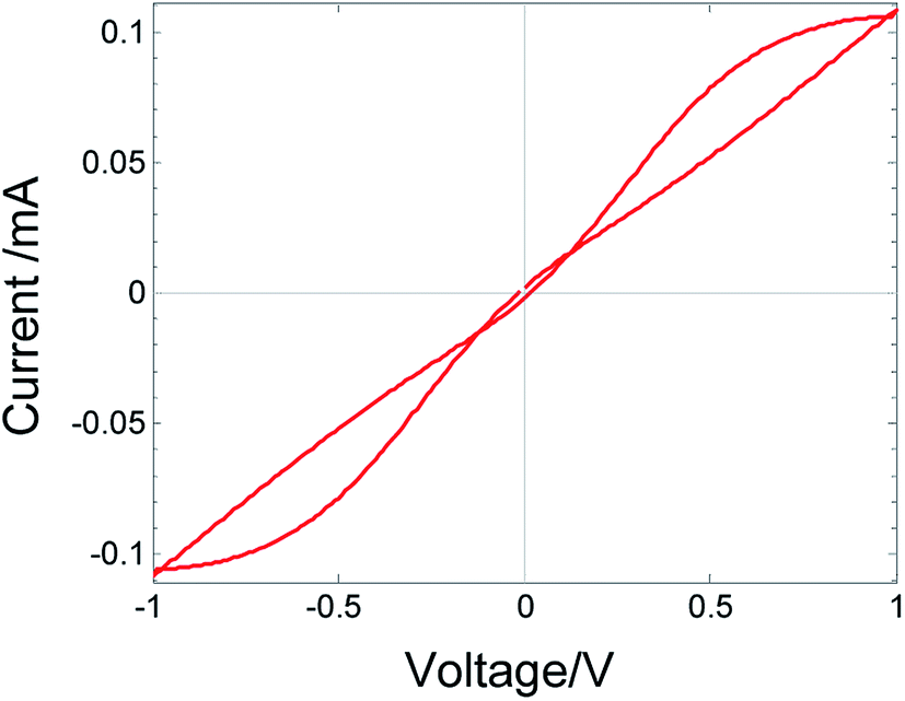
Metal/oxide/metal devices exhibit a diversity of I–V relations, among others, negative differential resistance (NDR); the latter takes place when, chronologically, an increase in the applied voltage V is associated with a decrease in the current I or vice versa. In the presence of hysteresis, these two cases are not equivalent although in both cases, the differential resistance is negative, i.e. dV/dI < 0. The conditions under which NDR appears in solid-state systems can vary. (a) The charge carriers can be either only electronic (electron/hole) or both electronic and ionic. (b) In some systems, NDR may appear under both dc and ac conditions, and in other systems, it may appear only in transient phenomenon; hence it is not observed under dc conditions. (c) When NDR appears only under ac voltage, hysteresis is expected to form a generalized loop, as seen in Fig. 1. NDR may appear only while following the time evolution going along the loop clockwise or while going counter clockwise. This is related to the I–V curve shapes denoted as N-NDR and S-NDR.1 (d) The temperature may be constant or a change in temperature is required to produce the NDR. | ||
| Fig. 1 Plot of I–V relations. Blue solid line indicates the I–V relations measured on Au/MoO3−δ/Au device at 70 °C for different voltage sweep rates: (a) 5 × 10⁻², (b) 5 × 10⁻³, (c) 3 × 10⁻³, (d) 1.58 × 10⁻³, (e) 1 × 10⁻³ and (f) 5 × 10⁻⁴ V s−1 (frequency, f = 2.1 × 1 0−2, 1.25 × 10⁻³, 6.6 × 10⁻⁴, 4.2 × 10⁻⁴, and 2.1 × 10⁻⁴ Hz, respectively). Arrows show the time evolution, which indicate that the curves do not cross. Red dashed line: fitted theory with parameters given in Table 1 device A. | ||
A tunneling diode is a typical example of NDR with electronic only conduction.2–4 The applied voltage shifts the electron energy levels in one part of a junction versus the levels in the other part; this changes the transition probability of electrons between degenerate energy levels in the two parts. For a certain range of the applied voltage, the level alignment is reduced, the electron transition probability decreases, and dV/dI < 0. In this case, NDR takes place whether the voltage applied is dc or ac. Another example where NDR appears under both ac and dc conditions in an electronic conductor is the mechanism proposed by Simmons and Verderber,5 where electrons propagate in an impurity band. Electrons are injected via tunneling from the cathode to degenerate energy levels in the solid mostly in the conduction band above the impurity band. The applied voltage changes the bending as well as shifts the energy of the electron energy levels in the solid relative to the Fermi level in the cathode. The current vs. voltage curve reaches a maximum followed by a decrease with further increase in the voltage, exhibiting NDR.
A mechanism that is based on ionic motion and electron transfer and holds only under ac conditions is realized in cyclic voltammetry (CV) both in liquid and solid state electrochemistry. Hysteresis and peaks appear in the I–V curve.6–8 The decrease, e.g., in a peak for V > 0, yields dV/dI < 0 while V increases. Eventually, the current I increases for even higher voltages, resulting in an N-shaped NDR curve.1 The peaks in CV do not appear under dc conditions. The peaks are generated by the increased current required for oxidizing or reducing the ions in the electrolyte, and a decrease in the peaks, which leads to dV/dI < 0, takes place when the ions, to be oxidized or reduced, are depleted. Chronologically, the propagation along the hysteresis loop in CV is clockwise. The motion of ions in the electrolyte, which is an electron insulator, is required as the ions have to reach the electrodes where the electrochemical reaction takes place.
In recent years, hysteresis loops and NDR have been observed in metal/insulator/metal (MIM) nanodevices, in which a temperature change enables hysteresis and NDR.9,10 The insulator in MIM systems is, in many cases, an oxide that under an intense electric field may be reduced for a given voltage polarity and conduct oxygen vacancies and electrons. The current in the MIM results in an increase in temperature. The electron and ion conductivities as well as the rate of exchange of oxygen at the electrode increase with the increasing temperature; this enhances the rate of reduction. By this positive feedback, an increase in voltage leads to a nonlinear, rapid increase in the electron conductivity and current. Depending on the electrical circuit, S-shaped NDR may be observed.
Hysteresis loops with peaks and no I–V curve crossing were reported by Du et al. for a Pt/TiO2/TiN device.11 The I–V curve, starting from the origin, increases exponentially with voltage towards a peak. The peak is occasionally achieved via an abrupt current increase rather than an exponential increase. The exponential I–V relations are allocated to the tunneling of electrons in a defect band of oxygen vacancies or titanium interstitials, whereas the decrease in current, in the NDR section, is allocated to a space charge generated by electrons trapped in an insulating region near the cathode following the mechanism of Simmons and Verderber.5 Similar results are reported by Cao et al.12 for a Ag/Bi-GeSe2/Ag device with peaks in the current increasing exponentially as in tunneling, followed by NDR. No I–V curve crossing is observed. However, in some cases, the curves meet at the origin and overlap over the range [−0.5, 0.5] volts. Memory is demonstrated for 3000 seconds. An overlap (but no crossing) between two branches of a hysteresis loop at the origin of the coordinates is also reported for a PEDOT:PSS polymer device that exhibits memory for at least 5000 seconds.13 Li et al.14 have reported symmetric hysteresis loops with two NDR regions and no line crossing for Sr3Co2Fe24O41, TiO2, Al2O3, and glass in a metal/insulator/metal (MIM) configuration. The hysteresis loops appear only when the device is exposed to humidity. The explanation is that the NDR region is governed by a decomposition reaction of adsorbed water, whereas an exponential increase in the current beforehand is due to tunneling. Xu et al.15 observed no I–V curve crossing and, in some cases, two crossings for MIM devices based on La0.7Sr0.3MnO3−δ. Jeong et al.16 noticed that a Pt/TiO2/Pt device, tested in air, may show hysteresis with symmetrical peaks, two NDR regions, and no curve crossing under cyclic voltammetry during the first four cycles. Oxygen is expected to leave the oxide in the presence of the Pt electrode.
Herein, we report the I–V relations with hysteresis and NDR measured for the MIM, Au/MoO3−δ/Au. NDR does not appear under dc conditions. Under ac conditions, hysteresis and peaks appear in the I–V curve depending on the ac frequency, as shown in Fig. 1. The peaks in the I–V curve are not reached by an abrupt or exponential increase in the current as in the MIM devices reported by others,11,12,14 but by a moderate increase that is less than linear in voltage. Chronologically, the propagation along the hysteresis loop is clockwise. The temperature is constant. The oxide is a mixed ionic–electronic conductor (MIEC), and the mobile ionic defects are oxygen vacancies.17,18 Contrary to the case of CV, herein, neither a redox reaction nor a chemical reaction at the gold electrodes is the reason for the hysteresis and NDR. Herein, we discuss a different mechanism that leads to NDR and hysteresis and depends on the bulk property. NDR and hysteresis arise due to the dynamics of changes in the spatial distribution of the ions, which, in turn, affects the distribution of the electrons. These changes lead to conductivity changes which, for a certain range of voltage, yield dV/dI < 0.19,20 The aim of this study is to present new experimental data exhibiting hysteresis and NDR and show that the theory that provides an explanation based on changes in the spatial distribution of the charge carriers, is in full agreement with the measured I–V relations, their dependence on the ac signal frequency, the chronological propagation of the I–V curve, their N-shaped NDR, as well as the change in I–V relations with temperature.
2. Experimental methods
2.1. Sample preparation
Oxide layers of Au/MoO3−δ/Au devices (Fig. 2) were prepared via thermal evaporation (sublimation of MoO3) in vacuum using shadow masks. To obtain multiple devices, the bottom electrodes were 21.6 mm-long stripes of gold, and those at the top were only 3.75 mm long, positioned perpendicular to the bottom electrodes. The width of the stripe in both the bottom and top Au electrodes was 300 μm. The thickness was 180 nm, as measured by the Bruker NT1100 optical profiler. A device is obtained where two electrodes overlap. The device area is 3002 μm2. | ||
| Fig. 2 (a) Image of four Au/MoO3−δ/Au devices on a SiO2-coated silicon substrate. (b) Closer view of one of the four devices. (c) Schematics of the cross-section of the device. Thickness of the MoO3−δ layer: 250 nm; thickness of Au electrodes: 180 nm. (d) Example of a TVC with a scan rate of 5 × 10⁻² V s−1 (frequency, f = 2.1 × 10⁻² Hz). | ||
The bottom Au electrodes were deposited on an n-type silicon wafer, coated with an insulating layer of silicon dioxide (100 nm thicks). Multiple rectangle layers of MoO3, 2 × 2.8 mm2 in area and 250 nm in thickness, were deposited on the bottom gold electrodes where devices should be formed. For the oxide layer deposition, 99.5% (Pb 0.001%, Fe 0.0005%) pure powder of MoO3 (Riedel-de Haën) was evaporated from an alumina crucible. The substrate was kept at room temperature. During deposition, the optimal gas pressure was determined to be 10−4 mbar. This pressure yields non-stoichiometric, oxygen-deficient,21 films yet of sufficiently high resistivity suitable for the following tests. The oxygen loss δ in MoO3−δ is calculated to be ∼10−4 (see the ESI†). Films that were deposited at the pressures of 10−5 mbar or lower were of too low resistivity and not used for the present measurements. The oxide films are amorphous, as determined by XRD measurements (Fig. 3). This is consistent with other reports that demonstrate that deposition of MoO3 on a substrate at near room temperature results in amorphous films.1,22 After each evaporation step, vacuum was stopped, and the layers were exposed to ambient air for 10 min.
 | ||
| Fig. 3 XRD (Cu-Kα1, 0.1540562 nm) of a thermally evaporated MoO3−δ thin film (∼400 nm thick) on a glass substrate. Continuous (blue) line indicates the measured spectrum. Reference: vertical (red) lines – crystalline MoO3. | ||
In the final third step, the top Au electrodes, in the form of short stripes, were deposited in a direction perpendicular to that of the bottom electrodes, each on top of one oxide rectangle. This completed the preparation of multiple devices. The measurements were carried out for single MIM devices using Metrohm Potentiostat, Autolab PGSTAT302N.
Gold is known to poorly stick to oxides to the extent that even at elevated temperatures, it does not react with the oxide; rather, it forms isolated small crystals (beading).23 On applying a dc current, the gold layer is easily detached from MoO3−δ resulting in oxygen bubbles formed under the top gold electrode (anode); this indicates no significant interaction between the metal and oxide.
The n-type silicon substrate ensured uniform temperature distribution. To precisely control the temperature during the measurements, a custom-made, PID-controlled, hotplate contained in a thermally insulating box was constructed. The standard deviation of the temperature of the silicon substrate placed on the hotplate was less than 0.03 °C during measurement. This box also prevented the sample from light and allowed control over the atmosphere.
2.2. Electrical characterization
The measurements were conducted on Au/MoO3−δ/Au MIM devices in the form of thin layers, as shown in Fig. 2. The ratio of the thickness of the oxide film (250 nm) to its lateral size in a device (300 μm) is 1200. Thus, the current in the device is considered to be flowing in one direction, and the device is treated as one-dimensional. Changes in the ion and electron current densities and defect concentrations occur only along the direction perpendicular to the layers.Measurements of electrical I–V relations were carried out on single devices under triangular voltage cycles (TVC). The applied voltage is the same as in linear cyclic voltammetry (CV), as shown in Fig. 2d. To avoid misunderstanding and confusion with CV where a redox reaction is involved, we refer to the signal as TVC. The sweep rate of the TVC is in the range 5 × 10⁻⁴ to 5 × 10⁻² V s−1, which for a peak voltage of 0.6 V (2.4 V per cycle) corresponds to 2.1 × 10⁻⁴ to 2.1 × 10⁻² Hz. Measurements were conducted in the temperature range of 55–80 °C.
The dielectric constant (relative electrical permittivity) of the MoO3−δ layer was determined via impedance spectroscopy. The measurements were interpreted regarding the Au/MoO3−δ/Au device as a plate capacitor with known geometry.
3. Results and discussion
The reduced oxide MoO3−δ contains both electrons and mobile ionic defects, oxygen vacancies. In the pristine oxide, oxygen vacancies are introduced together with electrons during the preparation process. The concentration of other ionic defects, introduced as impurities or excited as other native ionic defects, is speculated to be negligible. The concentration of holes is neglected as compared to the concentration of electrons because of the wide band gap (∼3 eV) of MoO3.17,24,25 The electrons propagate as small polarons.26 Oxygen vacancies are native donors and, in the present case, they are mobile native donors. An oxygen vacancy can be doubly ionized. However, at low temperatures considered herein (up to 80 °C), the second ionization is expected to be quenched, as reported for several oxides at near room temperature.24,27,28 The work function of gold is lower than the work function and affinity of MoO3−δ.17,18,26 As a result, electrons accumulate in the bent conduction band of the oxide, forming a narrow space charge, and the electrode contacts are considered as low-resistance ohmic contacts with respect to electron transfer.Fig. 1 shows the measured I–V relations for Au/MoO3−δ/Au, at 70 °C for different frequencies (scan rate) of the TVC. The I–V relations vary significantly with the TVC frequency. At high frequency, the I–V relations are linear (ohmic) as the ionic defects (oxygen vacancies) cannot follow the changes in the applied voltage, i.e., they are quasi-frozen. At this frequency, the oxide acts as a resistor with a fixed ion distribution, which, however, needs not be uniform. As the frequency is reduced, ion displacement becomes significant. Owing to a difference in the response of ions and electrons to an applied voltage, hysteresis appears.29,30 Strong negative differential resistance develops, and the I–V curves do not cross. For even lower frequency, the hysteresis is significantly reduced, as shown in Fig. 4. Under a low scan rate, the process is quasi-static, the device is close to steady state, and the ion defect distribution adjusts to changes in the applied voltage for both increasing and decreasing voltages; hence, hysteresis disappears.
 | ||
| Fig. 4 Blue stars: quasi-static I–V relations measured on Au/MoO3−δ/Au at T = 70 °C, 33.3 min at each point, 26.14 hours in total. Red dashed line: model fitted with electrodes of high impedance for material exchange. | ||
The results presented in Fig. 4 support the claim that the Au electrodes show high impedance for material exchange. The experimental results are close to those predicted under dc conditions for electrodes blocking material transfer and of low impedance for electron transfer.31
Fig. 1 and 4 also show theoretical curve fitting. The theory has been previously developed by our group.30,31 The oxide is treated as an MIEC in which the mobile ions are singly charged donors. The donors represent the singly charged oxygen vacancy. Material exchange under the ambient atmosphere, i.e., oxygen exchange, is allowed; however, high impedance is experienced. The electrodes are ohmic for electron transfer, as abovementioned. The initial condition is determined by the equilibrium state under zero voltage and vanishing currents and is given by the corresponding concentrations of the electrons and oxygen vacancy distributions.
Fitting was performed to the experimental curve of lowest frequency, as shown in Fig. 1, optimized for the positive voltage part. Then, only the scan rate is changed in the simulations while fitting the other five curves. Despite any significant changes in the hysteresis, NDR, and the magnitude of the current, the theory can follow the change in the shape of the I–V relations with the scan rate. The good fit supports the theoretical model. It is important to emphasize that in the applied theory, the temperature as well as the mobility of ions and that of electrons are constant.
The theory applied for symmetric boundary conditions yields quite (anti) symmetric hysteresis curves for positive and negative voltages after two cycles. However, the experimental results shown in Fig. 1 and 4 show a certain a-symmetry. The theory can handle a-symmetries in the device due to differences in the rate of material exchange at the electrode, work functions, and ambient composition.20,30 In the present devices, only a difference in the material exchange rate may be expected between the bottom electrode applied onto a dense substrate and the top electrode exposed to the ambient. However, simulations with different exchange rates do not lead to a better fit. We suggest that the reason for the a-symmetry is different, probably stress in the oxide introduced during sample preparation, leading to a gradient in the standard chemical potential of the oxygen vacancies.
The impedance of the gold electrodes for oxygen exchange is high, but finite. Contrary to platinum electrodes, which enable relatively rapid oxygen migration through the grain boundaries or oxygen storage in them, the gold electrodes exhibit high impedance to oxygen migration.32–34 The most probable process for the slow oxygen exchange is that it occurs through the periphery of the 180 nm-thick gold electrodes. To follow possible exchange of oxygen with the ambient, the temperature was increased to 80 °C, and the measurements were extended to 20 cycles. Fig. 5 shows that the current gradually increases with time. Fig. 5a shows the measured I–V relations. Fig. 5b shows the measured current as well as the fitted, theoretical current vs. time. The increase in current reflects a decrease in the resistance. It is interpreted to be due to reduction of the oxide. As the TVC is both positive and negative in a symmetric manner, the net reduction indicates that the rate of reduction is higher than the rate of oxidation. The theory predicts this a-symmetry and gradual reduction, as well.
 | ||
| Fig. 5 (a) I–V relations measured under TVC on Au/MoO3−δ/Au at T = 80 °C (one per four cycles is shown). Voltage sweep rate: 5 × 10⁻⁴ V s−1. The resistance at the limit V → 0 decreases with time from 2835 Ω to 2270 Ω. (b) Same cyclic I–V measurements presented as current versus time (blue solid line). Dashed red line: fitted theory. | ||
In view of the low, but finite rate of change in composition with time for a device under a TVC at 80 °C, the I–V relations, as shown in Fig. 1, were measured at 70 °C during a narrow time window. They present the third cycle after which the scan rate was changed. On this short time scale and at the abovementioned relatively low temperature, the composition changes are negligible, whereas for the third cycle, the TVC already induces the cyclic I–V relations.
The oxygen exchange rate at the electrodes is low and has the following effect. On applying a dc voltage of 1.5 volt for a few minutes, macroscopic bubbles (not shown) are formed, which develop under both voltage polarities. From the cell construction (Fig. 2), it is apparent that the bubbles develop under the top gold electrode for a positive applied voltage and under the oxide layer for the opposite voltage polarity. The bubbles are expected to consist of trapped oxygen. Some of the bubbles explode, i.e., tear the gas blocking layers.
Fig. 6 shows the change in the I–V relations with temperature for a fixed scan rate of the voltage of 5 × 10⁻⁴ V s−1. The peak position moves to the left, to shorter times, as the temperature increases. The slope at low applied voltage increases. This is due to an increase in the electron conductivity with temperature. The motion of the peaks to the left is due to an even faster increase of the ion conductivity with temperature. For further discussion of the temperature-dependent results, see the ESI.†
 | ||
| Fig. 6 (a) Measured I–V relations of Au/MoO3−δ/Au device, at T = 60–75 °C. The voltage sweep rate is 5 × 10⁻⁴ V s−1 for all temperatures. (b) Fitted I–V relations using the parameters of device A in Table 1, changing the temperature, only. | ||
4. Effect of humidity
The low, but finite rate of oxygen exchange with the ambient raises the question of a possible impact of humidity in the ambient. Li et al.14 demonstrated strong dependence of the I–V relations on the humidity for an MIM with Ag electrodes on Sr3Co2Fe24O41, and Messerschmitt et al.35 demonstrated the same for Pt electrodes on StTiO3−x. We, on the other hand, did not notice any effect of humidity on the I–V relation for Au electrodes on MoO3−δ. The control measurement was conducted in a dry environment using silica gel in the closed test box. No notable change in the I–V curves with humidity was observed. A possible explanation is that the top Au electrode is inert with respect to water molecule adsorption and can block the direct access of water molecules to the oxide.5. Fitted parameters
The fitted parameters are summarized in Table 1, device A. The fitted parameters of another sample denoted as B are also included. The parameters of device B are very similar to those of device A. For further discussion on device B, see ESI.† εr, δ, νe, Ee,νe, νi, and Ee,νi are defined in the table. The electron conductivity σe refers to the equilibrium state. The characteristic electron concentration n0 is a uniform electron concentration in the oxide under equilibrium. The fitting yields n0 = 7 × 1018 cm−3. This concentration depends on the preparation conditions. It can be changed by preparing the oxide layer under a different oxygen partial pressure, i.e. it increases with the decrease in the oxygen pressure. nleft and nright are the electron concentrations at the boundaries of the oxide bulk beyond the narrow accumulation regions, where the bands are flat under equilibrium. nleft and nright are equal to n0. The length λD is determined by n0 following the Debye length definition. It is fixed, of the order of a few nanometers, and serves as a measure of length. K is the reaction constant of vacancy ionization under equilibrium. τ is the time constant of the ionization reaction while relaxing back to equilibrium. j0,left and j0,right are the exchange constants of the current densities of ions at the electrodes. Noutx,left, Noutx,right are the chemical boundary conditions in the ambient, at the electrodes, expressed by the concentration of neutral vacancies that would prevail in the nearby oxide under equilibrium.20,36
| Parameters | Device A | Device B | Units |
|---|---|---|---|
| σe – electron conductivity | 9.7 × 10⁻⁶ | 1.3 × 10⁻⁵ | Ω−1 cm−1 |
| Ea,σe – activation energy of σe | 0.44 | 0.44 | eV |
| εr – dielectric constant | 19 | 19 | — |
| n0 – characteristic electron concentration | 7 × 10¹⁸ | 4 × 10¹⁸ | cm−3 |
| δ – oxygen deficiency | 1.2 × 10⁻⁴ | 7 × 10⁻⁵ | — |
| λD = (εrε0kBT/q2n0)1/2 – scale length | 2.1 | 2.8 | nm |
| νe = σe/qn0 – electron mobility | 8.6 × 10⁻⁶ | 2 × 10⁻⁵ | cm2 V−1 s−1 |
| Ea,νe – activation energy of νe | 0.44 | 0.44 | eV |
| α = νe/νi – electron-to-ion mobility ratio | 4.75 × 10⁶ | 1.3 × 10⁷ | — |
| Ea,α – activation energy of α | −0.47 | −0.47 | eV |
| νi – ion mobility | 1.8 × 10⁻¹² | 1.55 × 10⁻¹² | cm2 V−1 s−1 |
| Ea,νi – activation energy of νi | 0.9 | 0.9 | eV |
| Di = kBTνi/q – ion diffusion coefficient | 5.3 × 10⁻¹⁴ | 4.6 × 10⁻¹⁴ | cm2 s−1 |
| K – donor ionization reaction constant | 1.43 × 10⁻²² | 2.5 × 10⁻²² | cm3 |
| τ – donor ionization relaxation time | 1.7 × 10⁻⁷ | 1.3 × 10⁻⁷ | s |
| nleft = nright – electron concentrations near the accumulation regions | 7 × 10¹⁸ | 4 × 10¹⁸ | cm−3 |
| Noutx,left = Noutx,right – effective neutral donor concentrations in ambient | 7 × 10¹⁵ | 4 × 10¹⁵ | cm−3 |
| j0,left = j0,right – ion-exchange current density of the electrodes | 1.4 × 10⁻¹² | 1.4 × 10⁻¹² | A cm−2 |
6. Further discussion on the I–V relations
The hysteresis reported herein appears to be due to two reasons. (a) There is a difference in the mobility of the ions (oxygen vacancies) and the conduction electrons. Usually, the mobility of the ions is a few orders of magnitude lower than that of the electrons. (b) The driving force acting on the ions is different from that acting on the electrons. The electrons are driven by the applied voltage, whereas the ions are driven by a combination of the applied voltage V and a difference in the Nernst voltage, Vth, which equals (up to a coefficient being the ion charge) to a difference, on the oxide, in the chemical potential of the chemical components from which the ions are derived.29,37 Thus, for oxygen ions, the latter is a difference in the chemical potential of atomic oxygen (for neutral oxygen vacancies, it is minus that value). For a uniform surrounding, Vth can still appear as it is generated by polarization within the oxide under an applied voltage when the electrodes exhibit poor material transfer. Hence, Vth changes with time.The peaks that appear at a certain range of frequencies (Fig. 1d–f) are due to a slow response of the ions to the applied voltage. Under the conditions where V = 0, the ion distribution is close to uniform and the same is the case for the electron distribution. As the voltage V increases, the electron current increases, but the ion (and electron) distribution, initially, hardly changes. Eventually, the ion distribution is changed to the long-term distribution, being depleted on the side which is under positive polarity.29 This leads to a corresponding depletion of electrons there, which increases the overall resistance and decreases the current, i.e., NDR appears. Significant hysteresis appears in the frequency range of 2 × 10⁻⁴ to 2 × 10⁻² Hz for the amplitude of 0.6 V at 70 °C. This provides an estimate of the relaxation time of the hysteresis in the range of 50–5000 s, typically 500 s.
In Fig. 1d–f, for V > 0, the curve shape for voltage increase is different from the shape for voltage decrease. The reason is the immediate history, i.e., different ion distribution for the same applied voltage in the first and second quarters of a cycle.30 A similar difference is observed for V < 0.
As voltage increases, the I–V curve starting at the origin goes below the linear I–V relations, eventually turning into an NDR. There is a slow increase in the current with voltage in contrast to the experimental results on other devices,11–14,38 where the I–V curve increases exponentially with the voltage and, in some cases, even exhibits an abrupt increase. The region of NDR, as shown in Fig. 1d–f, 5 and 6, chronologically starts when the voltage increases at a high current and ends at a lower current. When the voltage range is wide enough, the current beyond the NDR region goes through a minimum and then increases again for even higher voltages, as shown in Fig. 5 and 6 (for 75 °C). This corresponds to N-shaped NDR.1
The I–V curve passes close to the origin of the coordinates (V = 0, I = 0) for all frequencies shown in Fig. 1. However, following the time evolution of the I–V relations, it is apparent that the curves do not self-cross and they do not pass through the origin. The non-crossing at the origin is due to residual polarization and finite ion mobility and current, as shown before via simulations.19,20,30 The deviation of the I–V curve from the origin is small in the present case due to the small ion mobility, which is about seven orders of magnitude lower than the electron mobility (see Table 1).
No long-term memory is experimentally observed. By long-term memory (referred to below for short as memory), we mean that different resistance values induced under high voltage are remembered when the voltage is set to zero for a long time, which is a few orders of magnitude longer than the characteristic relaxation time of the hysteresis. In the present case one would look for memory longer than 103 s. None was observed. This is consistent with the non-crossing at the origin of the I–V curve as shown hereinafter.
The current density through the device under the time-varying voltage consists of three components, je, ji and jD, where je is the electron current density, ji is the current density of the ions, and jD = ε0εr∂E/∂t is the displacement current (ε0 – permittivity of the vacuum, E – electrical field). The sum jt = je + ji + jD is uniform.30 For TVC of low frequency for which the displacement current can be neglected, jt = je + ji. All the frequencies, f, referred to in Fig. 1 are low, f ≪ 1 Hz, and the displacement current can be neglected. This can be inferred from the frequency dependence of the I–V curve.19
We show next that crossing of the origin by the I–V curve (i.e., I = 0 ↔ V = 0) is a necessary condition for memory under V = 0. It is first shown that memory in the present type of MIM devices is due to freezing of the ion distribution, i.e., the ion mobility is vanishing small. The resistance for electron current then reflects the frozen ion distribution, and different ion distributions yield different resistances. If the ion mobility does not vanish, the ion distribution changes as a driving force on ions exists despite the fact that V = 0. The driving force is due to the polarization mentioned earlier in this study. Thus, if the ions are mobile, the polarization can relax under V = 0, the ion distribution returns to one and the same value and so does the resistance. Then, there is no memory.
Crossing of the origin by the I–V curve is a necessary condition since if memory exists, ji vanishes under V = 0 and jt = je. The electron current density je has to vanish under V = 0 since when je is the sole component of the current, it must be uniform, which leads to je ∝ V.37,39 Hence, for V = 0, I ∝ jt = 0, i.e., when memory exists, the I–V curve has to cross the origin. Crossing of the origin is realized either by self-crossing of the I–V curve there or by overlap at the origin of the upper and lower branches of the hysteresis curve. Hence, vanishing of the ion mobility under V = 0 is a necessary condition for memory.
Crossing of the origin (V = 0, I = 0) is not a sufficient condition for the existence of memory as for V = 0 only an integral vanishes:  and je may be finite, non-uniform.20 jt ∝ I = 0 leads to ji = −je and hence to
  , i.e., the ion current does not vanish when the I–V curve crosses the origin. It is only the integral that vanishes; hence, memory is not assured when the I–V curve crosses the origin, i.e., crossing the origin is not a sufficient condition for memory.
The necessary condition is demonstrated by the fact that the I–V curves in Fig. 1 do not cross the origin, which is consistent with the finding that no memory is observed. The ion mobility in the present model has a fixed value. The fact that I–V curve crossing at the origin is not a sufficient condition is supported by the report of Aoki et al.40 on an MIM-based on GaOx. They have shown that crossing at the origin occurs in simulations of the I–V relations. As the mobility in their simulations does not vanish at low voltage, no long term memory is expected.
We now discuss the I–V curves in the dc limit and in the high-frequency limit. When the ion mobility does not vanish for V = 0, as is the case herein; and the voltage changes very slowly with time, then the voltage-induced polarization can relax and disappear while the applied voltage is reduced back to zero. Thus, there is no driving force for ion motion under V = 0 and the total current, which reduces only to the electron motion, vanishes for V = 0. Therefore, under dc condition, in contrast to the ac condition, in a uniform surrounding, the I–V curve crosses the origin. If the surrounding were not uniform, current would arise under zero voltage due to the chemical gradient and allowed material exchange at the electrodes as the exchange current density, j0, is finite. This is similar to a battery or fuel cell that is short circuited.37,39 On the other hand, in the limit of high frequencies (beyond those shown in Fig. 1), the displacement current cannot be neglected due to charging of the metal electrodes, and the current does not pass through the origin.20,29
In the calculated I–V relations, fitted to the measured I–V relations in Fig. 1, the curves do not self-cross. However, the same theoretical model, also under symmetric boundary conditions, can lead to self-crossing, but outside the origin. For a symmetric device and under working conditions (i.e., anti-symmetric TVC), the number of crossing points is even. This is shown in Fig. 7, where the parameters for the simulation are as shown in Table 1 device A, except that the thickness is only d = 25 nm instead of 250 nm (enhanced driving forces) and the mobility ration α = νe/νi = 47.5 instead of 4.75 × 10⁶. This type of crossing was observed experimentally by Xu et al.15 The current at V = 0 does not vanish, indicating the absence of the necessary conditions for memory. This is expected for a model with finite ion mobility.
 | ||
| Fig. 7 Simulated I–V relations with two crossings calculated for metal/MIEC/metal device with electrodes of high impedance for material exchange: d = 25 nm; α = 47.5; other parameters as in Table 1, device A. | ||
An a-symmetry in the device construction (different work function of the metal electrodes and different exchange rate of the material at the electrodes), a difference in the surroundings, as well as an a-symmetry in the voltage applied (different positive and negative amplitudes and different sweep rates of the decreasing and increasing voltages) can introduce self-crossing of the I–V curve, but not at the origin.20,30 The number of points of self-crossing, in this case, is odd. The self-crossing is sensitive to the TVC frequency and can be eliminated by increasing the frequency.20 Self-crossing outside the origin does not fulfill the necessary conditions for memory.
The strong dependence of the I–V relations on the frequency of the TVC is typical to the present system. These changes are absent in devices that exhibit rapid current changes (switching).40–43 There, the shape of the I–V relations is fixed by the switching process with only minor changes for a frequency change of ×25 (ref. 43) and even for a frequency change of five orders of magnitude.40
7. Conclusions
Triangular voltage cycles (TVC) of 0.6 V amplitude on Au/MoO3−δ/Au MIM devices at 55–80 °C show nonlinear I–V relations, short-term hysteresis, and negative differential resistance (NDR), but no curve crossing and long-term memory. The hysteresis depends on the TVC frequency and disappears for two opposing limits under dc conditions and for the highest frequency applied. The dc I–V relations are nonlinear. Hysteresis and NDR are explained on the basis that the insulator in MIM turns into a mixed ionic–electronic conductor via reduction, exhibiting mobile ions (oxygen vacancies) and electrons. The ions and electrons have constant mobility and the electrodes allow only slow oxygen transfer. An increase in the resistance with voltage during a voltage cycle as well as a decrease, resulting in NDR, are shown to exist when the ion and electron currents are controlled by drift diffusion at constant temperature. Chronologically, the propagation along the hysteresis loop is clockwise. The NDR is N-shaped. A fixed, finite ion mobility does not allow long-term memory as the latter requires vanishing small ion mobility for V → 0. A necessary condition for long-term memory is that the I–V curve crosses the origin under a low-frequency TVC for which the displacement current is negligible. It is sometimes experimentally difficult to decide whether the curve passes strictly through the origin. This limitation is due to relatively low ion mobility. Thus, seemingly crossing the origin may be misleading.The Au electrodes act as material blocking on the time scale of a few cycles of the applied TVC. However, the oxide composition changes slowly under longer TVC. This results in a slow decrease in the resistance of the oxide. The decrease in resistance occurs due to reduction of the oxide. Reduction takes place despite the application of both positive and negative voltages in a symmetric manner because the rate of reduction is higher than that of oxidation. The model allows interpretation of the slow changes in the oxide stoichiometry via exchange of oxygen with the ambient.
The close fit between the theoretical model and the experimental results enables extraction of parameters of the device (oxide and electrodes), as summarized in Table 1. Among others, the mobility of singly charged oxygen vacancies is determined near room temperature. This suggests a novel approach for the determination of ion mobility that may be applied to a wide variety of oxide MIM systems.
Acknowledgements
This research was supported by Israel Science Foundation, ISF, under grant No. 699/11.References
- A. L. Pergament, V. P. Malinenko, L. A. Aleshina, E. L. Kazakova and N. A. Kuldin, J. Exp. Phys., 2014, 2014, 951297 CrossRef.
- L. Esaki, Phys. Rev., 1958, 109, 603–604 CrossRef CAS.
- S. M. Sze and K. K. Ng, Physics of Semiconductor Devices, John Wiley & Sons, Inc., NJ, 3rd edn, 2007 Search PubMed.
- A. F. Volkov and S. M. Kogan, Phys.-Usp., 1969, 11, 881–903 CrossRef.
- J. G. Simmons and R. R. Verderber, Proc. R. Soc. London, Ser. A, 1967, 301, 77–102 CrossRef CAS.
- R. G. Compton and C. E. Banks, Understanding Voltammetry, World Scientific, Singapore, 2007 Search PubMed.
- S. Tappertzhofen, S. Menzel, I. Valov and R. Waser, Appl. Phys. Lett., 2011, 99, 203103 CrossRef.
- S. Tappertzhofen, H. Mündelein, I. Valov and R. Waser, Nanoscale, 2012, 4, 3040 RSC.
- A. Shkabko, M. H. Aguirre, I. Marozau, T. Lippert and A. Weidenkaff, Appl. Phys. Lett., 2009, 95, 152109 CrossRef.
- E. Yalon, S. Cohen, A. Gavrilov and D. Ritter, Nanotechnology, 2012, 23, 465201 CrossRef CAS PubMed.
- Y. Du, H. Pan, S. Wang, T. Wu, Y. P. Feng, J. Pan and A. T. S. Wee, ACS Nano, 2012, 6, 2517–2523 CrossRef CAS PubMed.
- M. Cao, B. Cheng, L. Xiao, J. Zhao, X. Su, Y. Xiao and S. Lei, J. Mater. Chem. C, 2015, 3, 5207–5213 RSC.
- V. C. Nguyen and P. S. Lee, Sci. Rep., 2016, 6, 19594 CrossRef CAS PubMed.
- J. Li, H. Zhang, G. Shao, B. Wu and S. Ouyang, EPL, 2014, 108, 27005 CrossRef.
- Z. T. Xu, K. J. Jin, C. Wang, H. Bin Lu, C. Wang, L. Wang and G. Z. Yang, Appl. Phys. A: Mater. Sci. Process., 2011, 105, 149–152 CrossRef CAS.
- D. S. Jeong, H. Schroeder and R. Waser, Phys. Rev. B: Condens. Matter Mater. Phys., 2009, 79, 1–10 Search PubMed.
- M. T. Greiner, L. Chai, M. G. Helander, W. M. Tang and Z. H. Lu, Adv. Funct. Mater., 2012, 22, 4557–4568 CrossRef CAS.
- M. T. Greiner, L. Chai, M. G. Helander, W. M. Tang and Z. H. Lu, Adv. Funct. Mater., 2013, 23, 215–226 CrossRef CAS.
- A. Leshem, E. Gonen and I. Riess, Nanotechnology, 2011, 22, 254024 CrossRef CAS PubMed.
- D. Kalaev and I. Riess, Solid State Ionics, 2014, 262, 883–888 CrossRef CAS.
- C. Battaglia, X. Yin, M. Zheng, I. D. Sharp, T. Chen, S. Mcdonnell, A. Azcatl, C. Carraro, B. Ma, R. Maboudian, R. M. Wallace and A. Javey, Nano Lett., 2014, 14, 967–971 CrossRef CAS PubMed.
- P. F. Carcia and E. M. McCarron, Thin Solid Films, 1987, 155, 53–63 CrossRef CAS.
- E. Shaffir, Y. Kauffmann and I. Riess, Acta Mater., 2014, 79, 59–65 CrossRef CAS.
- C. Julien, A. Khelfa, O. Hussain and G. Nazri, J. Cryst. Growth, 1995, 156, 235–244 CrossRef CAS.
- M. Kröger, S. Hamwi, J. Meyer, T. Riedl, W. Kowalsky and A. Kahn, Appl. Phys. Lett., 2009, 95, 4–7 CrossRef.
- I. K. Naik and T. Y. Tien, J. Phys. Chem. Solids, 1978, 39, 311–315 CrossRef CAS.
- J. He, R. K. Behera, M. W. Finnis, X. Li, E. C. Dickey, S. R. Phillpot and S. B. Sinnott, Acta Mater., 2007, 55, 4325–4337 CrossRef CAS.
- D. Gryaznov, E. Blokhin, A. Sorokine, E. A. Kotomin, R. A. Evarestov, A. Bussmann-Holder and J. Maier, J. Phys. Chem. C, 2013, 117, 13776–13784 CAS.
- I. Riess and A. Leshem, Solid State Ionics, 2012, 225, 161–165 CrossRef CAS.
- D. Kalaev and I. Riess, Solid State Ionics, 2013, 241, 17–24 CrossRef CAS.
- Y. Gil, O. M. Umurhan and I. Riess, Solid State Ionics, 2007, 178, 1–12 CrossRef CAS.
- R. Yang, K. Terabe, T. Tsuruoka, T. Hasegawa and M. Aono, Appl. Phys. Lett., 2012, 100, 1–5 Search PubMed.
- J. Joshua Yang, F. Miao, M. D. Pickett, D. a. a. Ohlberg, D. R. Stewart, C. N. Lau and R. S. Williams, Nanotechnology, 2009, 20, 215201 CrossRef CAS PubMed.
- M. Wojtyniak, K. Szot, R. Wrzalik, C. Rodenbücher, G. Roth and R. Waser, J. Appl. Phys., 2013, 113, 083713 CrossRef.
- F. Messerschmitt, M. Kubicek and J. L. M. Rupp, Adv. Funct. Mater., 2015, 25, 5117–5125 CrossRef CAS.
- D. Kalaev and I. Riess, Solid State Ionics, 2012, 212, 26–42 CrossRef CAS.
- I. Riess, in CRC Handbook of Solid State Electrochemistry, ed. P. J. Gellings and H. J. M. Bouwmeester, CRC Press, Inc, 1997, pp. 223–268 Search PubMed.
- D. S. Jeong, H. Schroeder, U. Breuer and R. Waser, J. Appl. Phys., 2008, 104, 123716 CrossRef.
- I. Riess, J. Phys. Chem. Solids, 1986, 47, 129–138 CrossRef CAS.
- Y. Aoki, C. Wiemann, V. Feyer, H.-S. Kim, C. M. Schneider, H. Ill-Yoo and M. Martin, Nat. Commun., 2014, 5, 3473 Search PubMed.
- D. Ielmini, F. Nardi and S. Balatti, IEEE Trans. Electron Devices, 2012, 59, 2049–2056 CrossRef CAS.
- J. P. Strachan, A. C. Torrezan, F. Miao, M. D. Pickett, J. Joshua Yang, W. Yi, G. Medeiros-Ribeiro and R. Stanley Williams, IEEE Trans. Electron Devices, 2013, 60, 2194–2202 CrossRef CAS.
- M. Kubicek, R. Schmitt, F. Messerschmitt and J. L. M. Rupp, ACS Nano, 2015, 9, 10737–10748 CrossRef CAS PubMed.
Footnote |
| † Electronic supplementary information (ESI) available. See DOI: 10.1039/c7ra06334b |
| This journal is © The Royal Society of Chemistry 2017 |