
 Open Access Article
 This Open Access Article is licensed under a Creative Commons Attribution-Non Commercial 3.0 Unported Licence
Significantly enhanced thermoelectric performance of Cu-doped p-type Bi0.5Sb1.5Te3 by a hydrothermal synthesis method†
Zichen Weiab,
Chenyang Wanga,
Li Youa,
Shijie Zhaoab,
Kang Yangb,
Haiyan Chen *b,
Jun Luo*a and
Xiaoyuan Chenb
*b,
Jun Luo*a and
Xiaoyuan Chenb
aSchool of Materials Science and Engineering, Shanghai University, Shanghai 200444, China. E-mail: junluo@shu.edu.cn
bThin Film Optoelectronic Technology Center, Shanghai Advanced Research Institute, Chinese Academy of Sciences, Shanghai 201210, China. E-mail: chenhy@sari.ac.cn; Tel: +86 21 20350846
First published on 23rd August 2017
Abstract
Cu-doped p-type Bi0.5Sb1.5Te3 compounds have been prepared by a facile hydrothermal method. X-ray powder diffraction analysis shows that the lattice parameter decreases with the Cu content, indicating that Cu+ ions are distributed on the crystal site of Bi/Sb, which is further confirmed by the p-type conducting behavior of the Cu-doped Bi0.5Sb1.5Te3. With the addition of Cu, the hole carrier concentration increases, and meanwhile the lattice thermal conductivity decreases. Furthermore, the greatly raised hole carrier concentration effectively suppresses the bipolar effect, which is beneficial for improving the thermoelectric properties. A dimensionless thermoelectric figure of merit (ZT) value of ∼1.2 at room temperature is achieved for the sample with 0.6 wt% Cu (nominal composition), and the ZT value increases with the temperature to ∼1.5 at 150 °C. Cu-doped Bi0.5Sb1.5Te3 samples exhibit most excellent thermoelectric performance among the presently available (Bi,Sb)2Te3-based materials, implying great potential as near room temperature thermoelectric materials.
Introduction
With the progress and development of human society, energy shortage has been a crisis issue nowadays. Thermoelectric materials are environmentally friendly energy-saving materials, which can directly convert heat into electricity (Seebeck effect) or vice versa (Peltier effect).1,2 The conversion efficiency of a thermoelectric device is measured by the dimensionless thermoelectric figure of merit (ZT) of the material| ZT = Sσ2T/κ, | (1) |
Bi2Te3-based materials3–9 are classical room-temperature thermoelectric materials. Both p-type (BixSb1−x)2Te3 (ref. 10 and 11) and n-type Bi2Se3−yTey (ref. 6 and 12–14) present excellent thermoelectric performance and have been put into commercial applications, which are well known as the most efficient thermoelectric materials operating near room temperature.15,16 According to literature reports, the Bi0.5Sb1.5Te3 alloy possesses the highest ZT value in all Bi2−xSbxTe3 solid solutions.17,18 Many methods have been attempted to fabricate Bi2Te3-based materials, e.g. ball milling,19–21 sintering22,23 and hot deformation.24–27 However, sample preparation needs a long time by most of the synthesis methods.17,28–31 Instead, hydrothermal synthesis as an effective method to fabricate Bi2Te3-based materials takes much shorter time,32,33 while the synthesis of a single-phase Bi0.5Sb1.5Te3 solid solution by hydrothermal reaction is rarely reported.18,34,35 Furthermore, the reported room-temperature thermoelectric properties of the Bi2Te3-based alloy synthesized by the hydrothermal method are not as good as expected.18,35,37 Therefore, it is desirable to develop a facile hydrothermal method to prepare an ideal single-phase Bi0.5Sb1.5Te3 alloy with optimized thermoelectric properties.
In this work, Cu-doped Bi0.5Sb1.5Te3 samples have been prepared by a facile hydrothermal method. According to the result of structure analysis, single-phase alloys with excellent thermoelectric properties have been successfully synthesized. A room-temperature ZT value as high as ∼1.2 has been achieved for the sample doped with nominal 0.6 wt% Cu, and its maximum ZT value of ∼1.5 is obtained at 423 K. To our knowledge, the nominal 0.6 wt% Cu-doped Bi0.5Sb1.5Te3 sample synthesized by a hydrothermal method in our experiments exhibits the most excellent thermoelectric performance among the presently available (Bi,Sb)2Te3-based materials, showing the great potential as near room temperature thermoelectric material.
Experimental
All samples were prepared via a facile hydrothermal method. High-purity powders of SbCl3 (Adamas 99%), BiCl3 (Adamas 99%+), Te (Adamas 99.999%) and Cu (Adamas 99.9%) were weighed according to stoichiometric Bi0.5Sb1.5Te3 + x wt% Cu (x = 0.0, 0.6, 1.6, 2.6). In a polytetrafluoroethylene (PTFE) cylindrical container, the raw materials were dissolved in deionized water with the aid of ultrasonication. Organic complexing additive ethylene diamine tetraacetic disodium salt (Greagent ≥ 99%) and the dispersant N2H4 (Adamas 80% Aq.) were added to previous solution. Then the pH value of the solution was adjusted to 11 by adding NaOH (Greagent ≥ 96%). The final filling ratio of solution inside the PTFE container is up to 80%. After 1 h of ultrasonication at room temperature, the PTFE container with the solution was transferred into a drying oven with a vacuum chamber and then heated at 180 °C for 48 h. The obtained powders were washed by the de-ionized water and then dried at 70 °C for 5 h. The obtained samples were marked as S1 (x = 0), S2 (x = 0.6), S3 (x = 1.6) and S4 (x = 2.6), respectively. For thermoelectric measurement, as-prepared powders were hot pressed at 350 °C for 30 minutes to acquire pellets.X-ray powder diffraction (XRD) patterns were collected on a Bruker AXS D8 Advance Diffractometer with Cu Kα radiation (λ = 0.154056 nm) using the continuous scanning method with a scanning voltage of 40 kV and a scanning speed of 0.01° per step. The morphologies of the samples were observed on a Hitachi S-4800 scanning electron microscope (SEM). LSR-3/1100 thermoelectric measurement system was used to measure the Seebeck coefficient and resistivity. The thermal diffusivity of the sample was detected by a laser flash diffusivity method on a Netzsch Laser Flash Apparatus (LFA) 1000. The total thermal conductivity κ was calculated by the equation κ = DρCp, where D, ρ and Cp were the thermal diffusivity, the mass density and the volumetric specific capacity of the sample, respectively. Cp was measured by a Netzsch differential scanning calorimetry (DSC) 201F1 instrument, and ρ by the Archimedes-method.
Results and discussion
Fig. 1 shows the XRD patterns of the samples S1–S4. The sample S4 with nominal 2.6 wt% Cu can be solely indexed to a single phase of rhombohedra Bi0.5Sb1.5Te3 (PDF#49-1713). For the samples S1, S2 and S3, only a trace amount of unknown second phase appears as the impurities, indicating that the Cu-doped Bi0.5Sb1.5Te3 solid solution as the main phase has been successfully synthesized. There are three kinds of possible positions for Cu ions in the crystal structure of Bi0.5Sb1.5Te3, namely, lattice site, interstitial site and interlayer position. If Cu+ enters the interstitial site or interlayer position, the lattice constant should increase with the Cu content. However, as shown in Table 1, the lattice constant a of the Cu-doped Bi0.5Sb1.5Te3 samples decreases with the Cu concentration. Therefore, the decrease of the lattice constant a can be attributed to the partial replacement of Bi3+/Sb3+ by Cu ions because the radius of Cu+ (0.77 Å) is smaller than the average radius of Bi3+/Sb3+ (1.03/0.76 Å). On the other hand, for the Cu-doped samples, the c-axis parameter remained nearly constant within the standard deviations as the Cu content increases, implying that Cu ions only replace Bi3+/Sb3+ but not go to the interlayer position. The crystal site of Cu ions in the structure can be further verified by the Hall effect measurement. According to Hall effect measurement, the Cu-doped Bi0.5Sb1.5Te3 samples show p-type conducting behavior. Fig. 2 shows the dependence of the carrier concentration on the Cu content for all Bi0.5Sb1.5Te3 samples. The hole concentration increases with the Cu doping content, indicating that the Cu+ ion, acting as an acceptor, enters the lattice to replace part of Bi3+/Sb3+ ions, which is consistent with the conclusion reported by Hao et al.38 Otherwise, the Cu-doped Bi0.5Sb1.5Te3 samples should exhibit n-type conducting behavior if the Cu+ ion goes into the interstitial site or interlayer position.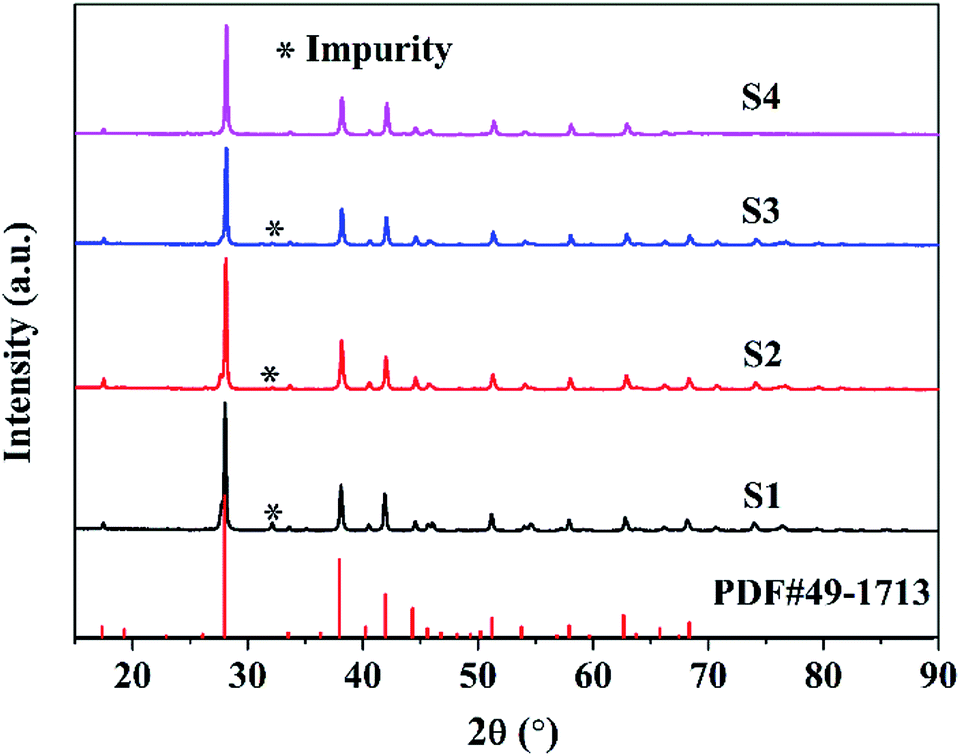 | ||
| Fig. 1 XRD patterns of the samples S1–S4. (Nominal Cu contents of S1, S2, S3 and S4 are 0 wt%, 0.6 wt%, 1.6 wt% and 2.6 wt%, respectively). | ||
| Samples | Nominal Cu content x (wt%) | a (Å) | c (Å) | V (Å3) |
|---|---|---|---|---|
| S1 | 0 | 4.3094 (±0.0016) | 30.487 (±0.0007) | 490.31 (±0.0020) |
| S2 | 0.6 | 4.3015 (±0.0011) | 30.473 (±0.0006) | 488.31 (±0.0015) |
| S3 | 1.6 | 4.2986 (±0.0018) | 30.466 (±0.0009) | 487.53 (±0.0025) |
| S4 | 2.6 | 4.2914 (±0.0024) | 30.473 (±0.0011) | 486.00 (±0.0030) |
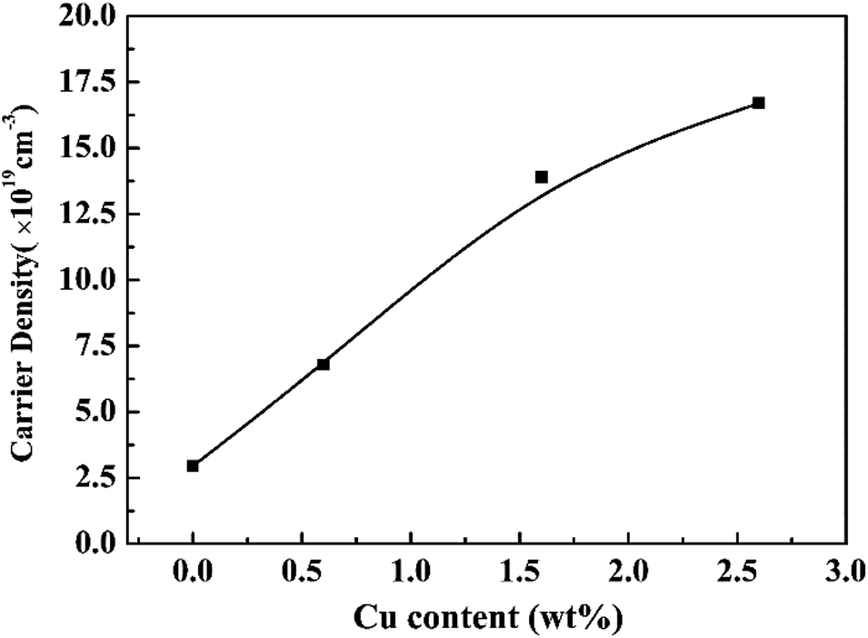 | ||
| Fig. 2 Room-temperature hole carrier concentration as a function of the nominal Cu content for all Bi0.5Sb1.5Te3 samples. | ||
To further explore the structural feature of Cu-doped Bi0.5Sb1.5Te3, the morphologies of the as-prepared powder and hot-pressed bulk sample have been observed by SEM. Fig. 3a and b show the SEM images of sample S3, exhibiting the feature of small particle sizes. As shown in Fig. 3a, most of the particles are at the nanoscale, typically on the order of several hundreds of nanometers. Furthermore, some mesoscale hexagonal platelets with the particle sizes from 1 to 10 micrometers are observed in Fig. 3a, which should relate to the anisotropic crystal structure of Bi0.5Sb1.5Te3. The Bi2Te3 compound has a rhombohedra structure32 with the space group R![[3 with combining macron]](https://www.rsc.org/images/entities/char_0033_0304.gif) m, wherein along the c-axis, the atomic layers array in the order of –Te(1)–Bi–Te(2)–Bi–Te(1)– and the neighboring Te(1) layers are linked by weak van der Waals bonds.34–37 Therefore, the morphology of Bi2Te3-based alloy normally exhibits the feature of hexagonal platelets. For the powders obtained in our work, under the control of hydrothermal synthesis, most of grains are nanoparticles with deficient crystallinity, while only a small number of grains are well-crystallized, existing as hexagonal platelets. This could also explain the isotropic properties of these samples (see Fig. S1 and S2†). As shown in Fig. 3b, the small particle size is maintained after hot pressing (the feature of small particle size can also be observed from the cross section of the bulk, shown in Fig. S3†). Hence, the small particle size as well as numerous grain boundaries of the samples synthesized by the hydrothermal method could contribute to the reduced lattice thermal conductivity around room temperature, which is beneficial for the Cu-doped Bi0.5Sb1.5Te3 aiming at room-temperature applications.
m, wherein along the c-axis, the atomic layers array in the order of –Te(1)–Bi–Te(2)–Bi–Te(1)– and the neighboring Te(1) layers are linked by weak van der Waals bonds.34–37 Therefore, the morphology of Bi2Te3-based alloy normally exhibits the feature of hexagonal platelets. For the powders obtained in our work, under the control of hydrothermal synthesis, most of grains are nanoparticles with deficient crystallinity, while only a small number of grains are well-crystallized, existing as hexagonal platelets. This could also explain the isotropic properties of these samples (see Fig. S1 and S2†). As shown in Fig. 3b, the small particle size is maintained after hot pressing (the feature of small particle size can also be observed from the cross section of the bulk, shown in Fig. S3†). Hence, the small particle size as well as numerous grain boundaries of the samples synthesized by the hydrothermal method could contribute to the reduced lattice thermal conductivity around room temperature, which is beneficial for the Cu-doped Bi0.5Sb1.5Te3 aiming at room-temperature applications.
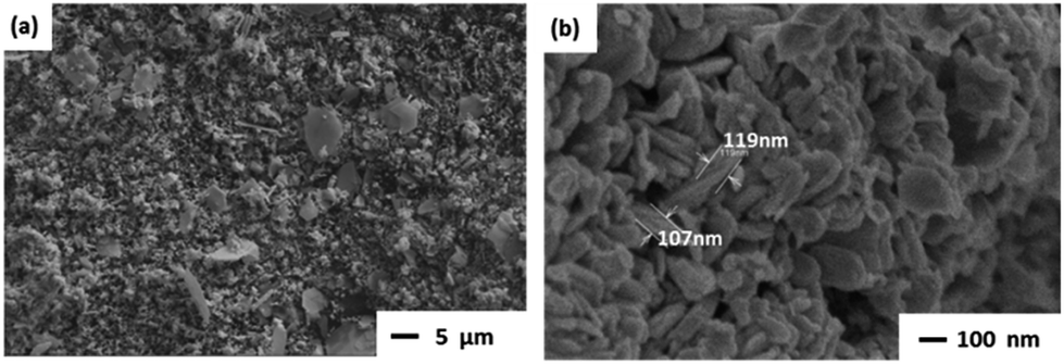 | ||
| Fig. 3 Typical SEM images of (a) the as-prepared powders and (b) ground powders after the hot pressing of sample S3. | ||
Fig. 4 shows the electrical transport properties of the undoped and Cu-doped Bi0.5Sb1.5Te3 samples. As shown in Fig. 4a, the Seebeck coefficients of all the samples are positive, further confirming their p-type conducting behavior. The room-temperature Seebeck coefficient decreases with the Cu content because of the increased carrier concentration. For the undoped sample S1, its Seebeck coefficient decreases with the increasing temperature, which can be ascribed to the bipolar effect caused by the intrinsic excitation below room temperature.30,35 For the Cu-doped samples S2–S4, their room temperature Seebeck coefficients decrease with the increase of Cu content, which can be attributed to increased hole concentration by substituting of Cu for Bi/Sb. Furthermore, their temperature-dependent Seebeck coefficients show the typical behavior of a degenerate semiconductor. As shown in Fig. 4a, for samples S2–S4, the Seebeck coefficient firstly increases linearly with the increasing temperature, but linear trend of the Seebeck curve is suppressed by the bipolar effect at elevated temperature. It is obvious that the bipolar effect of the Cu-doped samples shifts to higher temperature because the mixed conduction is suppressed by increasing hole concentration. Thus, comparing with the undoped sample, the Seebeck coefficients of the Cu doped samples increase dramatically in the temperature range of 150–350 °C.
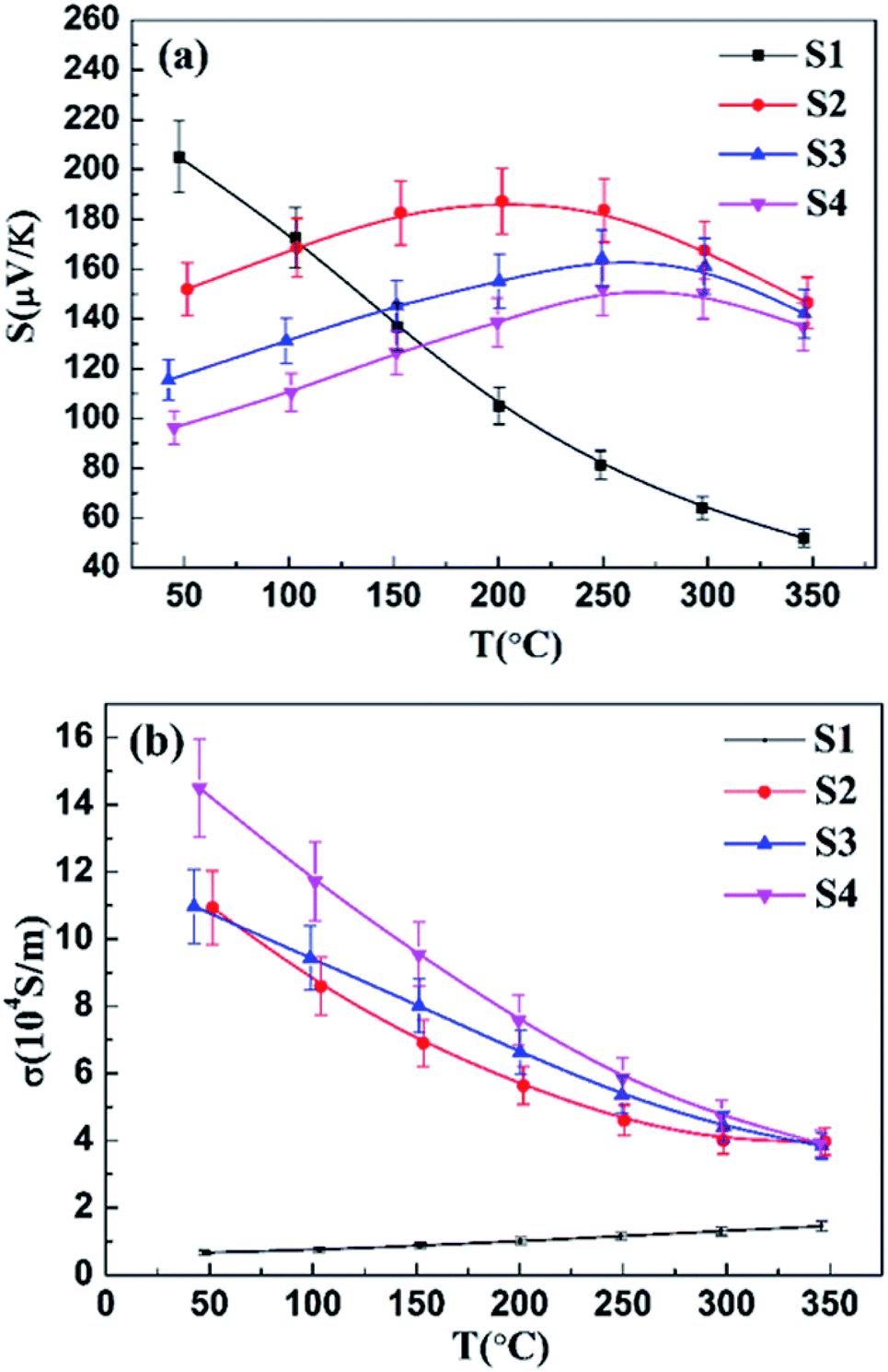 | ||
| Fig. 4 Temperature-dependences of (a) Seebeck coefficient and (b) electrical conductivity of undoped and Cu-doped samples. | ||
As shown in Fig. 4b, the temperature-dependent electrical conductivity of the undoped sample S1 also shows the conducting behavior of intrinsic excitation, i.e. the electrical conductivity increases with the increasing temperature. For the Cu-doped samples, their electrical conductivities firstly decrease rapidly with the raised temperature, and then decrease slowly with the temperature due to the mixed conduction. The slowly decrease of electrical conductivity at high temperature for all the samples can be ascribed to the bipolar effect. Furthermore, the doping of Cu increases the hole concentration, which effectively suppresses the bipolar effect and shifts the intrinsic excitation temperature to higher temperature. It is worth to note that the σ values of the Cu-doped samples prepared via a facile hydrothermal method in our work could be comparable to that of Bi–Sb–Te alloys synthesized by conventional sintering methods,30,39 indicating this facile hydrothermal method is an effective route for developing high-performance (Bi,Sb)2Te3-based materials.
It should be pointed out that the room-temperature electrical conductivity is almost the same for the samples S2 and S3. To clarify this, Hall carrier concentration and mobility have been measured. As listed in Table 2, the hole concentration of sample S3 is almost twice of that of the sample S2, while its mobility is nearly half of that of the latter one. Hence, these two samples have similar electrical conductivity at room temperature. The reduced carrier mobility of the sample S3 could be ascribed to the enhanced carrier scattering in two aspects: (1) more lattice point defects produced by Cu substitution and (2) increased hole concentration.
| Samples | Nominal Cu content x (wt%) | n (1019/cm3) | μ (cm2 V−1 s−1) |
|---|---|---|---|
| S2 | 0.6 | 6.7792 | 60.7478 |
| S3 | 1.6 | 13.9000 | 29.2516 |
The combination of raised Seebeck coefficient and increased electrical conductivity results in a power factor of ∼25 μW cm−1 K−2 at 50 °C for sample S2 (Fig. 5), which is nearly 9 times as large as that of sample S1. The power factor decreases to 23 μW cm−1 K−2 at 150 °C and remains as high as ∼8.5 μW cm−1 K−2 at 350 °C for sample S2. Furthermore, the power factors of Cu-doped samples are always much larger than that of undoped sample in the measured temperature range from 50 °C to 350 °C.
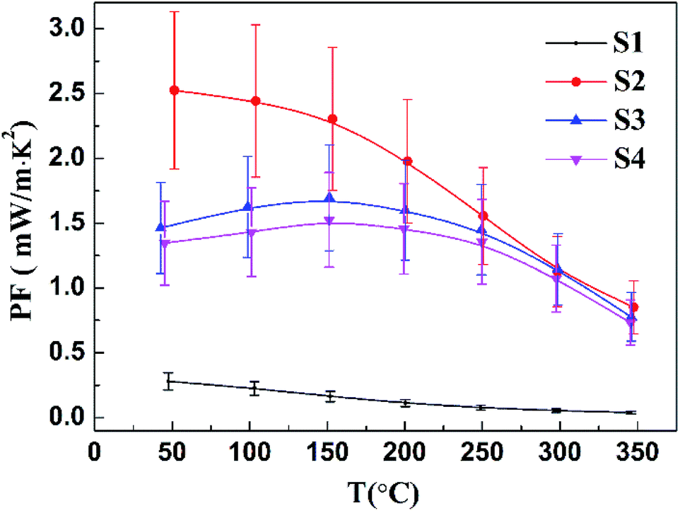 | ||
| Fig. 5 Power factor as a function of temperature for undoped and Cu-doped samples. | ||
Fig. 6 shows the temperature-dependent thermal conductivity of samples S1–S4. It is obvious that all the samples have very low thermal conductivities. As shown in Fig. 6, the thermal conductivity of sample S1 increases with the increasing temperature, which could be ascribed to the increased electronic contribution to the total thermal conductivity caused by the bipolar effect. Similarly, for the Cu-doped samples, the increase of the thermal conductivity at high temperature can also be attributed to intrinsic excitation.
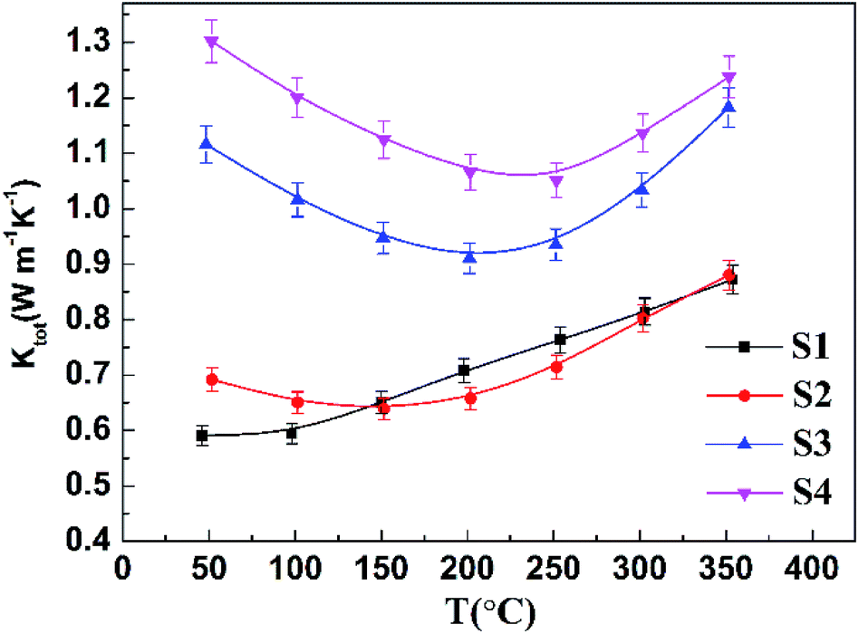 | ||
| Fig. 6 Temperature-dependent thermal conductivity for undoped and Cu-doped samples. | ||
The thermal conductivity of Cu-doped samples S2–S4 is higher than that of the undoped sample S1 owing to the dramatically increased electronic thermal conductivity, since the hole concentration is significantly enhanced with the Cu content.
For undoped sample S1, compared with those synthesized by mechanical alloying19 and spark plasma sintering (SPS),39 its nanostructuring obtained by hydrothermal synthesis lowers the thermal conductivity by about 31–50% at room temperature, due to the contribution of additional phonon scattering, implying that our hydrothermal synthesis method is effective on reducing the thermal conductivity. As for sample S2, its average thermal conductivity in the temperature range of 150–350 °C is about 0.71 W m−1 K−1, approximately 12%, 21% and 22% reduction than those of Cu-doped Bi–Sb–Te samples reported by Lee et al.,17 Hao et al.38 and Cui et al.,30 respectively. The low thermal conductivity of sample S2 can be ascribed to different defects: nanoscale grains by hydrothermal synthesis, atomic-scale point defects of Cu substitution for Bi3+/Sb3+, and the presence of second phase. It is worth to note that, in p-type Bi0.5Sb1.5Te3 materials, the Cu dopants not only increase the hole concentration, but also introduce nanostructural defects, which were also observed in SPS-treated Cu-doped Bi0.5Sb1.5Te3 bulk samples.38
Fig. 7 presents the ZT values for the undoped and Cu-doped samples. The ZT value of sample S1 decreases with the increasing temperature, which can be explained by a drastic reduction of the Seebeck coefficient due to the bipolar effect. The doping of Cu effectively suppresses the bipolar effect by increasing the hole concentration, leading to a shift of the peak ZT value to higher temperature with the raised Cu concentration. Obviously, the ZT values of the samples with Cu doping are much larger than those of the undoped sample, even though the total thermal conductivity is enhanced after the Cu doping. Therefore, the huge enhancement of ZT from 50 °C to 350 °C is mainly contributed from the power factor afforded by doping. However, with the further increased Cu content, the ZT value decreases, which probably originates from the increased electronic contribution to the thermal conductivity due to the increasing electrical conductivity. The sample with nominal 0.6 wt% Cu exhibits the best thermoelectric performance because of the appropriate doping level, small grain size, as well as the presence of trace amount of impurities. Finally, a ZT value of 1.2 around room temperature and a peak ZT value of ∼1.5 at 150 °C are achieved for the sample S2. The average ZT value of sample S2 in the temperature range of 50–200 °C is about 1.4, ∼40% improvement of that of the commercial Bi2Te3 ingot materials. It should be noted that, by the Cu doping, the optimum operating temperature is decreased and the working temperature range becomes broader, making Cu-doped bismuth antimony telluride based alloys have better prospects for commercial applications.
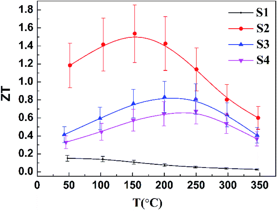 | ||
| Fig. 7 Temperature dependence of ZT values for undoped and Cu-doped samples. | ||
Conclusions
In this work, the Cu-doped p-type Bi0.5Sb1.5Te3 compounds have been successfully synthesized by a facile hydrothermal method. Structural analysis indicates that the sample crystallizes into rhombohedra structure and the Cu+ ions enter the crystal lattice by substituting partial Bi3+/Sb3+, which is further confirmed by the electrical properties measurement. The doping of Cu effectively suppresses the bipolar effect of Bi0.5Sb1.5Te3 compound by increasing the hole concentration, leading to the improved electrical transport properties and increased power factor. The main contribution to the huge enhancement of ZT from 50 °C to 350 °C is the power factor afforded by Cu doping. The sample doped with nominal 0.6 wt% Cu shows a ZT value of ∼1.2 around room temperature and a peak ZT value of ∼1.5 at 150 °C, originating from the combined effect of appropriate doping level, small grain size, and the presence of uniformly dispersed trace amount of impurities.Conflicts of interest
There are no conflicts of interest to declare.Acknowledgements
This work was supported by National Natural Science Foundation of China (Grant No. 51201108, 11174308, 51371194, and 51632005) and Knowledge Innovation Project of the Chinese Academy of Sciences (Grant No. KGCX2-EW-315).References
- A. Majumdar, Science, 2004, 303, 777–778 CrossRef CAS PubMed.
- J. Yang, L. Xi, W. Qiu, L. Wu, X. Shi, L. Chen, J. Yang, W. Zhang, C. Uher and D. J. Singh, npj Comput. Mater., 2016, 2, 15015 CrossRef CAS.
- Y. L. Chen, J. G. Analytis, J. H. Chu, Z. K. Liu, S. K. Mo, X. L. Qi, H. J. Zhang, D. H. Lu, X. Dai, Z. Fang, S. C. Zhang, I. R. Fisher, Z. Hussain and Z. X. Shen, Science, 2009, 325, 178–181 CrossRef CAS PubMed.
- Y. Y. Li, G. Wang, X. G. Zhu, M. H. Liu, C. Ye, X. Chen, Y. Y. Wang, K. He, L. L. Wang, X. C. Ma, H. J. Zhang, X. Dai, Z. Fang, X. C. Xie, Y. Liu, X. L. Qi, J. F. Jia, S. C. Zhang and Q. K. Xue, Adv. Mater., 2010, 22, 4002–4007 CrossRef CAS PubMed.
- M. Scheele, N. Oeschler, K. Meier, A. Kornowski, C. Klinke and H. Weller, Adv. Funct. Mater., 2009, 19, 3476–3483 CrossRef CAS.
- H. Zhang, C.-X. Liu, X.-L. Qi, X. Dai, Z. Fang and S.-C. Zhang, Nat. Phys., 2009, 5, 438–442 CrossRef CAS.
- H. Goldsmid, Materials, 2014, 7, 2577–2592 CrossRef CAS PubMed.
- F. Li, X. Huang, W. Jiang and L. Chen, J. Electron. Mater., 2013, 42, 1219–1224 CrossRef CAS.
- B. Poudel, Science, 2008, 320, 634–638 CrossRef CAS PubMed.
- D. Kong, Y. Chen, J. J. Cha, Q. Zhang, J. G. Analytis, K. Lai, Z. Liu, S. S. Hong, K. J. Koski, S. K. Mo, Z. Hussain, I. R. Fisher, Z. X. Shen and Y. Cui, Nat. Nanotechnol., 2011, 6, 705–709 CrossRef CAS PubMed.
- W. Xie, S. Wang, S. Zhu, J. He, X. Tang, Q. Zhang and T. M. Tritt, J. Mater. Sci., 2012, 48, 2745–2760 CrossRef.
- S. Wang, W. Xie, H. Li and X. Tang, Intermetallics, 2011, 19, 1024–1031 CrossRef CAS.
- S. Wang, W. Xie, H. Li and X. Tang, J. Phys. D: Appl. Phys., 2010, 43, 335404 CrossRef.
- W. Liu, K. C. Lukas, K. McEnaney, S. Lee, Q. Zhang, C. P. Opeil, G. Chen and Z. Ren, Energy Environ. Sci., 2013, 6, 552–560 CAS.
- F. Hao, P. Qiu, Y. Tang, S. Bai, T. Xing, H.-S. Chu, Q. Zhang, P. Lu, T. Zhang, D. Ren, J. Chen, X. Shi and L. Chen, Energy Environ. Sci., 2016, 9, 3120–3127 CAS.
- G. Tan, L. D. Zhao and M. G. Kanatzidis, Chem. Rev., 2016, 116, 12123–12149 CrossRef CAS PubMed.
- K.-H. Lee, H.-S. Kim, S.-I. Kim, E.-S. Lee, S.-M. Lee, J.-S. Rhyee, J.-Y. Jung, I.-H. Kim, Y. Wang and K. Koumoto, J. Electron. Mater., 2012, 41, 1165–1169 CrossRef CAS.
- C.-J. Liu, G.-J. Liu, C.-W. Tsao and Y.-J. Huang, J. Electron. Mater., 2009, 38, 1499–1503 CrossRef CAS.
- Z. Wang, A. Vemishetti, J. I. Ejembi, G. Wei, B. Zhang, L. Wang, Y. Zhang, S. Guo, J. Luo, C. Chepko, Q. Dai, J. Tang and G.-L. Zhao, Mater. Sci. Eng., B, 2016, 205, 36–39 CrossRef CAS.
- Q. H. Yi Ma, B. Poudel, Y. Lan, B. Yu, D. Wang, G. Chen and Z. Ren, Nano Lett., 2008, 8, 2580–2584 CrossRef PubMed.
- T. Hayashi, M. Sekine and J. Suzuki, Mater. Trans., 2007, 10, 2724–2728 CrossRef.
- P. K. Nguyen, K. H. Lee, J. Moon, S. I. Kim, K. A. Ahn, L. H. Chen, S. M. Lee, R. K. Chen, S. Jin and A. E. Berkowitz, Nanotechnology, 2012, 23, 415604 CrossRef CAS PubMed.
- D. M. Lee, C. H. Lim, S. Y. Shin, D. C. Cho and C. H. Lee, J. Electroceram., 2006, 17, 879–883 CrossRef CAS.
- L. Hu, H. Wu, T. Zhu, C. Fu, J. He, P. Ying and X. Zhao, Adv. Energy Mater., 2015, 5, 1500411 CrossRef.
- L. Hu, T. Zhu, X. Liu and X. Zhao, Adv. Funct. Mater., 2014, 24, 5211–5218 CrossRef CAS.
- L.-P. Hu, T.-J. Zhu, Y.-G. Wang, H.-H. Xie, Z.-J. Xu and X.-B. Zhao, NPG Asia Mater., 2014, 6, e88 CrossRef CAS.
- T. Zhu, Z. Xu, J. He, J. Shen, S. Zhu, L. Hu, T. M. Tritt and X. Zhao, J. Mater. Chem. A, 2013, 1, 11589–11594 CAS.
- Z. Xu, H. Wu, T. Zhu, C. Fu, X. Liu, L. Hu, J. He, J. He and X. Zhao, NPG Asia Mater., 2016, 8, e302 CrossRef CAS.
- B. Madavali and S.-J. Hong, J. Electron. Mater., 2016, 45, 6059–6066 CrossRef CAS.
- J. L. Cui, H. F. Xue, W. J. Xiu, W. Yang and X. B. Xu, Scr. Mater., 2006, 55, 371–374 CrossRef CAS.
- W.-S. Liu, Q. Zhang, Y. Lan, S. Chen, X. Yan, Q. Zhang, H. Wang, D. Wang, G. Chen and Z. Ren, Adv. Energy Mater., 2011, 1, 577–587 CrossRef CAS.
- Z. L. Li, R. Y. Teng and S. Q. Zheng, J. Cryst. Growth, 2014, 406, 104–110 CrossRef CAS.
- Z. L. Li, Y. D. Chen and S. Q. Zheng, Nano Energy, 2016, 28, 78–86 CrossRef CAS.
- C.-J. Liu, G.-J. Liu, Y.-L. Liu and L.-R. Chen, J. Mater. Chem., 2012, 22, 4825 RSC.
- Y. Zhang, G. Xu, J. Mi, F. Han, Z. Wang and C. Ge, Mater. Res. Bull., 2011, 46, 760–764 CrossRef CAS.
- L. Zhu, H. Wang, Y. Wang, J. Lv, Y. Ma, Q. Cui, Y. Ma and G. Zou, Phys. Rev. Lett., 2011, 106, 145501 CrossRef PubMed.
- W. Ren, C. Cheng, Y. Xu, Z. Ren and Y. Zhong, J. Alloys Compd., 2010, 501, 120–123 CrossRef CAS.
- F. Hao, P. Qiu, Q. Song, H. Chen, P. Lu, D. Ren, X. Shi and L. Chen, Materials, 2017, 10, 251 CrossRef PubMed.
- S. D. Bhame, D. Pravarthana, W. Prellier and J. G. Noudem, Appl. Phys. Lett., 2013, 102, 211901 CrossRef.
Footnote |
| † Electronic supplementary information (ESI) available. See DOI: 10.1039/c7ra06277j |
| This journal is © The Royal Society of Chemistry 2017 |