DOI:
10.1039/C7RA06267B
(Paper)
RSC Adv., 2017,
7, 49883-49889
Enhanced thermoelectric properties of In2O3(ZnO)5 intrinsic superlattice ceramics by optimizing the sintering process
Received
5th June 2017
, Accepted 16th October 2017
First published on 26th October 2017
Abstract
Thermoelectric (TE) materials have a promising application as they can interconvert thermal energy to electrical energy directly. Oxide TE materials have attracted more attention for this application due to their high temperature stability. In this work, In2O3(ZnO)5 intrinsic superlattice ceramics with a layered structure were synthesized by reaction sintering a mixed powder of In2O3 and ZnO at 1200 °C for different holding times (t = 6, 8, 10, 12 and 15 h) in air. Their thermoelectric properties including the electrical conductivity, Seebeck coefficient and thermal conductivity, were measured from 323 to 973 K. The thermoelectric properties depended on the holding time. The highest ZT value of 0.19 at 973 K was obtained for the sample with a 12 h holding time.
1. Introduction
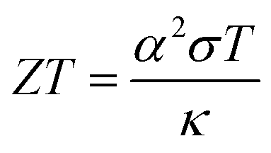
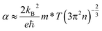
Thermoelectric (TE) energy conversion has received more attention in the past decade on account of its promising application to directly convert waste heat into electricity.1–4 This means that a huge amount of waste heat, including from human activities, can be converted into useful energy, helping to increase the production efficiency and improve living conditions. The TE figure-of-merit (ZT) is given bywhere σ, α, T and κ are the electrical conductivity, the Seebeck coefficient, absolute temperature and the thermal conductivity, respectively.5,6 According to the eqn (1), TE material which has good performance needs a large electrical conductivity, a Seebeck coefficient and a low thermal conductivity.
Semiconductor oxides are great prospective alternatives to conventional high temperature thermoelectric materials because of their high temperature stability and relatively wide bandgap. Currently, Si–Ge7 alloy and Yb14MnSb11 (ref. 8) have high ZT value in high temperature, all of which possess problems such as high cost and toxic raw materials, especially Ge, Yb and Sb. BiCuSeO9,10 maximum application temperature is 600 °C because of oxygen will disappear with the temperature increases. Therefore, the cheaper, high temperature stability and more environmental friendly TE materials are receiving increased attention.
ZnO has a wurtzite structure with space group P63m, belongs to the polar crystal classes.11 It is pyroelectric and piezoelectric what represents the basis for applications in electromechanical or thermoelectric coupling devices. Moreover, ZnO which with a direct bandgap of 3.37 eV at room temperature is a semiconductor. In2O3 is also a wide bandgap transparent semiconductor (Eg ≈ 3.6 eV) and has a high electrical conductivity.12–15 Indium is sixfold coordinated in the In2O3 bixbyite structure, while zinc adopts fourfold coordination in the ZnO wurtzite structure.16 The homologous compounds, In2O3(ZnO)k (k = integer), have very unique crystal structures with space groups of R3m (for k = odd) or P63/mmc (for k = even) and are composed of layers of InO3/2, InZnO5/2, and ZnO, what are stacked sequentially along the c-axis of the hexagonal system.17,18 We can learn a lot from quite many previous studies on the inherent n-type behavior in In2O3 and ZnO.19–23 The zincs disappear during the high temperature solid state reaction. So, the cation antisite defect, indium on zinc (InZn), also should be considered. VO-Zni defect in ZnO and VO-Ini in In2O3 for binaries are up to be the origin of n-type conductivity in un-doped ZnO and In2O3. In2O3(ZnO)5 intrinsic superlattice ceramics have three advantages for application in thermoelectric materials. First of all, it possesses excellent structure and chemical stability even at high temperature (under 800 °C). Secondly its wide band gap prevents thermal excitation of “minor” carriers and thus allow the ZT increases at high temperature forward. For the layered structure, the carrier mobility along the layer direction is higher than that cross the layer direction. Thirdly, In2O3(ZnO)5 has a very unique crystal structure composed of layers of InO2− and InZn5O6+, periodically stacking in the c-axis direction. This layered structure gives rise to low thermal conductivity which is attributed to the reduced mean free path of the phonon between layers.
In this work, the n-type In2O3(ZnO)5 intrinsic superlattice ceramics were fabricated by a standard solid reaction 1200 °C for 6 h, 8 h, 10 h, 12 h and 15 h. There are In2Zn7O10 impurity phase of 6 h, 8 h and 10 h. When the holding time is 15 h, the impurity phase appears in the sample and correspond well to In2Zn4O7. Only the 12 h sample contain supreme ZT value of 0.19 at 973 K. We have found the best sintering process of In2O3(ZnO)5. The resulting samples have an immense improvement over some other works.45–50 This is a good foundation of further optimizing In2O3(ZnO)5 thermoelectric performance in our next work.
2. Experiments
All samples, belonging to the In2O3(ZnO)k series, were prepared using a standard solid reaction route. Starting powders, In2O3 (Aladdin, 99.99%) and ZnO (Aladdin, 99.99%), were weighed in stoichiometric amounts and ground together by ball milling using agate balls and vial. The resulting powers were pressed uniaxially under 30 MPa, forming parallel disc with dimensions of 15 mm × 8 mm pellets. The pellets were transference into an alumina crucible and calcined at 1200 °C for 6–15 h.
The samples were characterized by X-ray diffraction (XRD: Cu-Kα Bruker D8, Germany) and the density (ρ) of the sample was determined by Archimedes method. The fractographs were measured by a scanning electron microscope (SEM, ZEISS, EVO 18-21-57).
The Seebeck coefficient and electrical resistance were measured using a Seebeck coefficient/electrical resistance measuring system (ZEM-3, Ulvac-Riko, Japan) in a He atmosphere (0.015 MPa pressure) which use the 2 × 2 × 8 mm cuboid sample. The Seebeck coefficient was calculated from thermoelectric voltage generated between both ends of a sample ΔV and temperature difference between the two ends ΔT. The thermal diffusivity (D) was measured by laser flash method (NETZSCH, LFA457, Germany) in flow argon atmosphere (80 ml min−1) which requires that the samples are discs with a diameter of 6 mm. The electrical and thermal properties of the samples were tested perpendicular to pressure direction. The Hall coefficients (RH) of the samples were measured at 293 K using a physical properties measurement system (HMS-7000), and a magnetic field of 2 T and electrical current of 30 mA were applied. The carrier concentration (ni) was calculated by ni = 1/eRH, where e is the electronic charge. The carrier mobility (μi) was calculated by μi = RH/ρ. The thermal conductivity (κ) was calculated from the density (ρ), specific heat and thermal diffusivity using the relationship κ = DCpρ. These thermoelectric properties were measured in the temperature range of 323–973 K.
3. Result and discussion
3.1 Phase and microstructure
Fig. 1 shows the schematic representation of crystal structure from [010] direction for In2O3(ZnO)5, parent oxides ZnO and In2O3 are also shown for comparison. Unit cells are marked by the blue lines. In the primitive cell of In2O3(ZnO)5 has 150 atoms.24 Both Zn and In atoms occupy the crystallographic positions. In other words, incorporation of In into ZnO slab is random, as is shown in the schematic representation of refined crystal structures (Fig. 1). In atomic ordered into the ZnO thin plate (i.e., “zigzag fringe”) has surveyed in previous studies and is thought to have a thermodynamic stability.25–27 This structure what configuration of In in ZnO slab in our case can be obtained by high temperature calcinations which using a dilatory cooling rate (∼5 °C). It is worthy to mention that the refined crystal structures of homologous compounds clearly indicate a close relationship to their parent oxides ZnO and In2O3.28 According to their distinct coordination numbers (k), we can identify easily the layers of wurtzite type and bixbyite type structure. Wurtzite type structure similar with ZnO is largely maintained in these homologous compounds although deviation from the trigonal-bipyramidal coordination (k = 5) occurs.
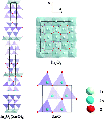 |
| | Fig. 1 Schematic representation of crystal structure from [010] direction for In2O3(ZnO)5, parent oxides ZnO and In2O3 are also shown for comparison. Unit cells are marked by the black lines. | |
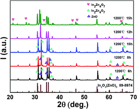
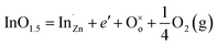
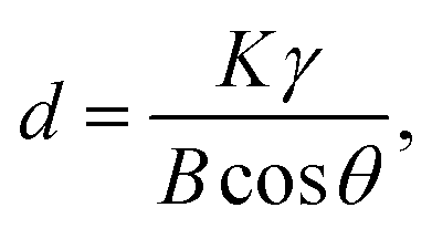
As the data in Table 1 indicate, the content of In decreased with the increase of holding time. And the In atomic ratio is 49.15% in the In2O3(ZnO)5 dispersed with 6 h, however, In2O3(ZnO)5 dispersed with 15 h bulk sample In atomic ratio decreased to 9.11%. Because heating for longer time results into potential loss of indium. The In2O3(ZnO)5 intrinsic superlattice ceramics were synthesized at 1200 °C for different holding time (6–15 h) as shown in Fig. 2. There are rhombohedral symmetry In2O3(ZnO)5 of all specimens, which corresponds well to the PDF#89-8974 card.29 These results are consistent with the previous reports that In2O3(ZnO)k crystallize in group R3m for odd k values and P63/mmc for even k values.30–32 Heating for longer time brings about potential loss of indium and zinc. There are In2Zn7O10 impurity phase in 6 h, 8 h and 10 h samples. In addition, there are ZnO impurity in the 6 h and 8 h sample. When the holding time is 15 h, the impurity phase appears in the sample and correspond well to In2Zn4O7. Only the 12 h holding time sample is In2O3(ZnO)5 pure phase. The crystallinity of all samples is showed in Table 2. As shown in Fig. 2, the peak intensity in 2θ ranges 30–47° for all the samples have obvious changes, indicating that there is texture in all the samples. As the holding time is 15 h, the B of peaks increased, indicating the grain refinement according the Debye–Scherrer formula,  33 (K is the Scherrer constant, d is the average thickness of the crystal grains perpendicular to the crystal plane direction, B is the diffraction width of the measured sample, θ is the diffraction angle, γ is the X-ray wavelength, 0.154056 nm).
Table 1 The elemental mapping were performed for In2O3(ZnO)5 with different holding time (t = 6, 8, 10, 12 and 15 h)
| Bulk samples |
Indium mass norm [%] |
Zinc mass norm [%] |
Oxygen mass norm [%] |
Indium atom [%] |
Zinc atom [%] |
Oxygen atom [%] |
Abs. error [%] |
Rel. error [%] |
| 6 h |
81.32 |
79.21 |
9.47 |
49.15 |
9.77 |
41.08 |
2.64 |
22.33 |
| 8 h |
40.19 |
49.35 |
10.46 |
16.65 |
40.89 |
42.46 |
3.55 |
16.09 |
| 10 h |
37.97 |
50.65 |
11.38 |
15.72 |
37.17 |
47.11 |
3.12 |
17.12 |
| 12 h |
33.04 |
49.79 |
17.17 |
13.02 |
34.58 |
47.94 |
2.16 |
9.18 |
| 15 h |
24.48 |
54.95 |
20.57 |
9.11 |
35.92 |
54.97 |
3.98 |
15.89 |
 |
| | Fig. 2 Observed X-ray diffraction patterns of In2O3(ZnO)5 at 1200 °C for 6–15 h holding time. | |
Table 2 The crystallinity of the samples sintered at different holding times (t = 6, 8, 10, 12 and 15 h)
| Sample |
6 h |
8 h |
10 h |
12 h |
15 h |
| Crystallinity (%) |
86.30 |
88.19 |
89.27 |
91.45 |
89.83 |
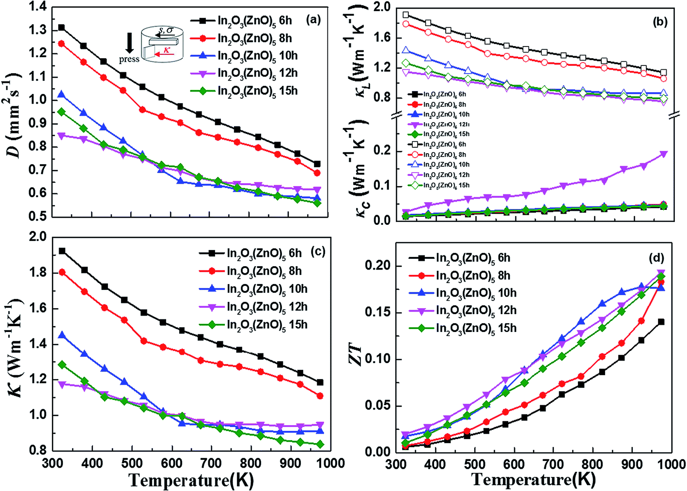
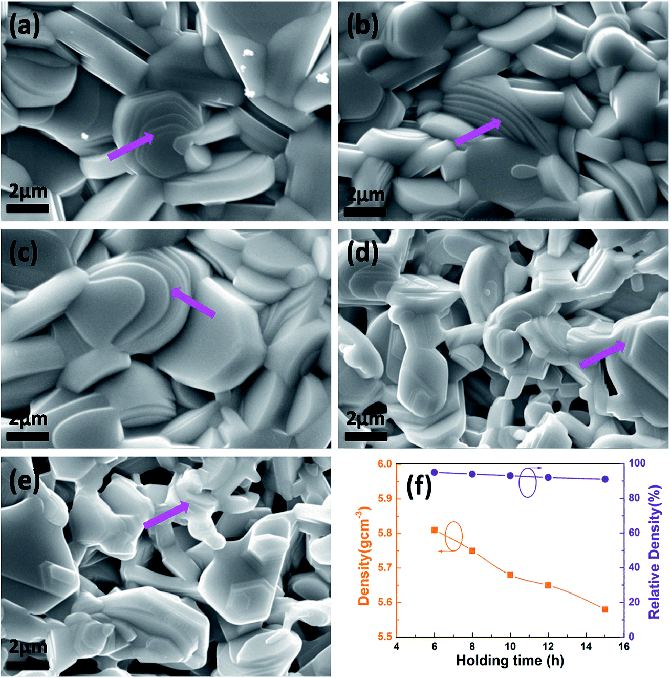
Fig. 3 shows the scanning electron microscopy (SEM) images of In2O3(ZnO)5 at 1200 °C for 6 h (a), 8 h (b), 10 h (c), 12 h (d), 15 h (e). From the Fig. 3 the grain distribution is relatively uniform. The powders were sintered to bulk at high temperature. The bulk samples have the large grain size of several micrometers. In other words, all the grains were observed with the sharp edge, and their layered structure was described in terraced fields (indicated by the purple arrow on the SEM images). The density of the samples shows the tendency of decreased with the increase of holding time, as is shown Fig. 3(f). It is because that as the extension of holding time from 6 h to 15 h, the In2O3(ZnO)5 ceramic samples possess more and more pores because of potential loss of indium and zinc.
 |
| | Fig. 3 The scanning electron microscopy images of In2O3(ZnO)5 at 1200 °C for 6 h (a), 8 h (b), 10 h (c), 12 h (d), 15 h (e); the density and relative density of at In2O3(ZnO)5 1200 °C for 6–15 h (f). | |
3.2 Thermoelectric properties
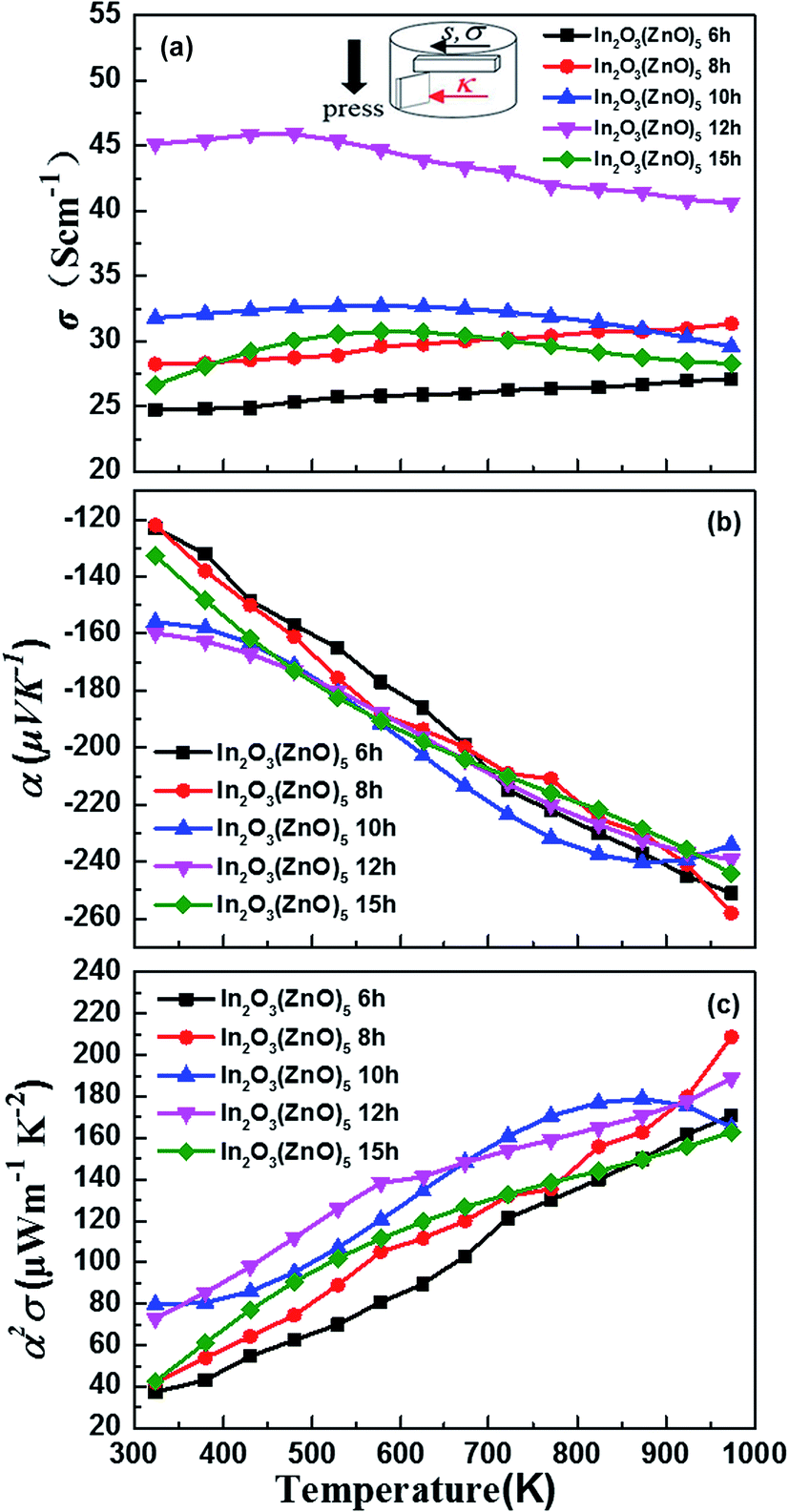
Fig. 4 shows that the temperature dependence of electrical transport properties for the In2O3(ZnO)5 ceramics at 1200 °C for 6–15 h. The electrical conductivity (σ) of 6 h and 8 h samples increased with the increasing temperature, being indicative of the semiconductor behavior in Fig. 4(a). When the holding time is 10 h, 12 h or 15 h, which σ decreased with the increasing temperature, showed a metallic behavior. As H. Ohta et al.43 research work shows that In2Zn7O10 and (ZnO)5In2O3 showed a metallic behavior and the pure ZnO showed a semiconductor behavior. Hence the 6 h and 8 h samples showed a metallic behavior, while the 10 h, 12 h and 15 h samples showed a semiconductor behavior. The concentration of conduction electrons is rather high and fixed in the present temperature range possibly. It is possibly induced by certain small deviations from stoichiometric compositions because the carrier concentration is determined by the valence control mechanism expressed as the following eqn (2),| |
 | (2) |
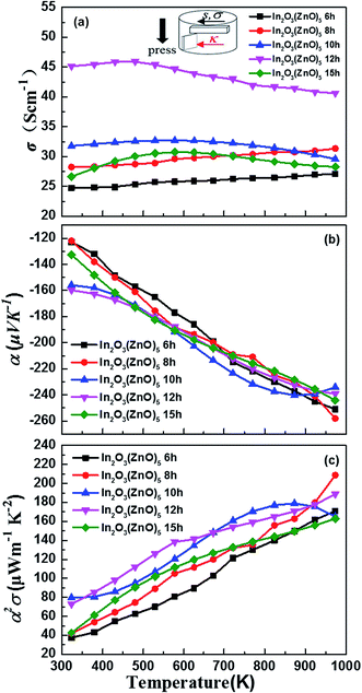 |
| | Fig. 4 The (a) temperature dependence of the electrical conductivity (σ), (b) the Seebeck coefficient (α), and (c) power factor (α2σ) for each bulk sample. | |
The σ depends on both carrier concentration n and mobility μ as the following eqn (3),
where
e is the electronic charge. The sample for 12 h show higher electrical conductivity than other holding time samples. As reported in previous work,
43 the electrical conductivity of In
2Zn
7O
10 is lower than the In
2O
3(ZnO)
5. Hence the electrical conductivity of 6 h, 8 h and 10 h samples lower than the 12 h sample. The space group of In
2Zn
4O
7 is
P6
3/
mmc, which structure is different with In
2Zn
4O
7 and In
2Zn
7O
10. We infer the existence of In
2Zn
4O
7 led the lower electrical conductivity. The sample of 12 h has the highest electrical conductivity due to its pure In
2O
3(ZnO)
5 which has the noticeably higher density of the InO
2− planar defects, representing highly conductive paths in the homologous phase. The holding time dependence of the carrier concentration (
ni) and the carrier mobility (
μi) at room temperature has shown in
Fig. 5. The extension of the holding time result into the potential loss of indium and zinc. Meanwhile indium substituted zinc and it produce electrons. Hence the carrier concentration increases with the extension of the holding time. The raised carrier concentration given rise to the reducing of carrier mobility in line with their calculation method. As shown in
Fig. 4(b), the Seebeck coefficients (
α) of all specimens were observed to be positive what account for ZnO–In
2O
3 ceramics are n-type semiconductor, meaning that the main carrier is electron. The absolute value of
α increased with the increasing of temperature within the scope of the measuring temperature, which corresponding to the electrical conductivity.
α is from the
eqn (4) obtained,
34| |
 | (4) |
where

is the Seebeck coefficient for a classical electron gas. The different holding times make different carrier concentrations of the samples. The temperature dependence of power factor (
σα2) for In
2O
3(ZnO)
5 (1200 °C for 6–15 h) bulks is shown in
Fig. 4(c). The material has high figure of merit who has large power factor. All the samples showed a similar positive temperature dependence of
σα2, despite having different slopes. With the increasing testing temperature, the power factor of the samples increased significantly because the Seebeck coefficient increased rapidly with temperature, and the power factor and the square of Seebeck coefficient were proportional. The maximum value of
σα2 of 209 μW m
−1 K
−2 was acquired for In
2O
3(ZnO)
5 (1200 °C, 8 h) at 973 K. In addition to In
2O
3(ZnO)
5 (1200 °C, 15 h), the
σα2 values of the specimens increased with increasing holding time.
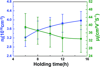 |
| | Fig. 5 The holding time dependence of the carrier concentration (ni) and the carrier mobility (μi) at room temperature. | |
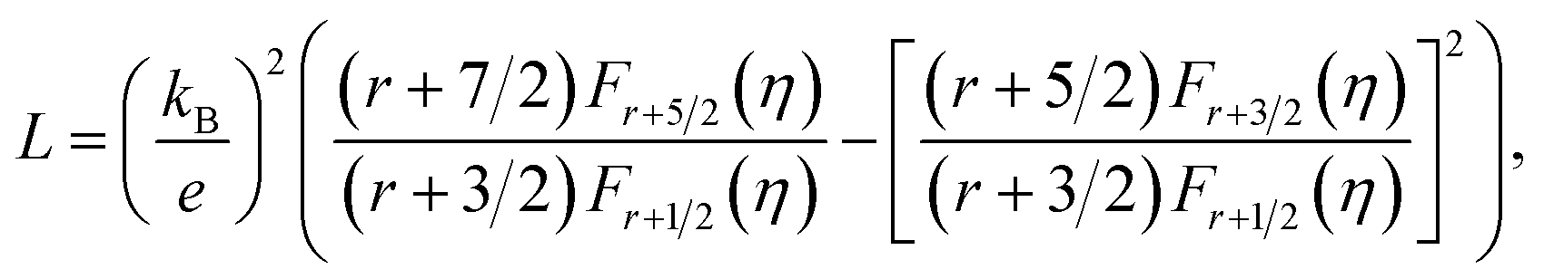
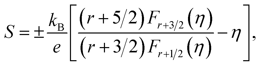
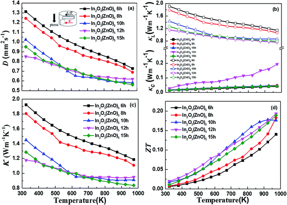
Fig. 6(c) exhibits the temperature dependence of the total thermal conductivity (κ) for all bulk samples, what the κ value was calculated from the thermal diffusivity (D) (Fig. 6(a)), the heat capacity (Cp), the density (ρ), and κ(κ = DCpρ). The κ decreased in the wake of holding time increasing. The thermal conductivity is presented by κ = κc + κL, κc is the thermal conductivity caused by electron transport and κL is the lattice thermal conductivity (Fig. 6(b)). κc is calculated by the Wiedemann Franz law, κc = LσT, where L, σ and T are Lorenz number, electrical conductivity and absolute temperature, respectively. Reduced Fermi energy was used to calculate Lorenz number (eqn (5)) varies as Seebeck value changes (eqn (6)) with temperature or composition. The L calculation was estimated in a traditional single parabolic band model (resulting in an L with a deviation of less than 10% as compared with a more rigorous single non-parabolic band and multiple band models calculation) as described in ref. 35 and 36, where the reduced Fermi energy was implicitly determined by the Seebeck values (eqn (2)).
| |
 | (5) |
| |
 | (6) |
 |
| | Fig. 6 The temperature dependence of thermal diffusivity (D) (a), the carrier thermal conductivity (κc) and the lattice thermal conductivity (κL) (b), the totally thermal conductivity (κ) (c) and ZT value (d) for all bulk samples. | |
The difference in thermal conductivity is the contribution of the low relative density and anisotropic structure of In2O3(ZnO)5. We assumed that interface scattering was generated by porosity and difference in local density which arises from the anisotropic structure. One major perspective of nanostructure engineering to enhance thermoelectric properties is to design and create the (defect) structure with appropriate length scale, which is smaller than the mean free path of phonons but larger than that of electrons or holes.37 The effect of superlattice structures on reducing thermal conductivity has been attributed to various mechanisms, including the modification of phonon spectrum,38 phonon localizations, phonon scatterings at interfaces due to acoustic mismatch or defects formed arising from lattice mismatch39 etc. It should be noted that phonon mean free path depends on both temperature and microstructural features, since temperature determines density of states of phonons and thereby affects phonon–phonon interactions/lattice imperfections introduce defect scatterings of phonons (eqn (7)).
| |
 | (7) |
Assuming the scattering mechanisms are additive, the total phonon mean free path can be written as ref. 40. Superlattice belong to a surface defect. According to Zhao et al.,41 its special layered structure introduces additional phonon scattering, reducing the mean free path of the phonon. Thereby the thermal conductivity of the samples is reduced. The values are agreement with the previous ones.42,43 In addition to the κ value of all samples are very low and have a little reduction along with the increase of temperature. The total thermal conductivity trend consistent with the lattice thermal conductivity makes clear that κL occupies a leading position. The temperature dependence of the thermoelectric dimensionless figure of merit, ZT, is shown in Fig. 6(d). As shown in the eqn (8),44
| |
 | (8) |
The supreme ZT value of 0.19 was measured for the 12 h holding time sample at 973 K.
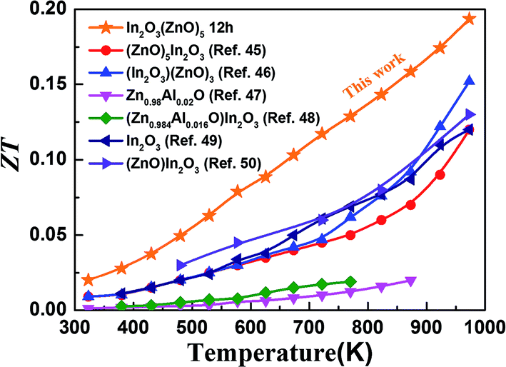
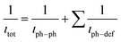
Fig. 7 shows the figure of merit of this work compared with other In2O3–ZnO system using different synthesis process. This work has an obvious improvement makes it an excellent candidate for further research and optimization for high-temperature thermoelectric applications.
 |
| | Fig. 7 The ZT value comparison of this work and other In2O3–ZnO system. | |
4. Conclusions
Intrinsic superlattice ceramics In2O3(ZnO)5 with layered structures were synthesized by reaction sintering mixed powders of In2O3 and ZnO at 1200 °C for different holding time, t = 6, 8, 10, 12 and 15 h, in air. There are In2O3(ZnO)7 impurity phase of 6 h, 8 h and 10 h samples. When the holding time is 15 h, the impurity phase appears in the sample and correspond well to In2O3(ZnO)4. Only the 12 h holding time sample is In2O3(ZnO)5 pure phase. They were dense and a number of stripes possibly corresponding to stacking faults were observed in every grain. This layered structure gives rise to low thermal conductivity due to it is attributed to the reduced mean free path of the phonon between layers. The thermoelectric ZT increasing with increasing temperature and holding time (6–12 h) with the exception of 15 h. The maximum figure of merit of 0.19 was detected for the 12 h holding time sample at 973 K. In2O3(ZnO)5 intrinsic superlattice ceramics were found be the huge potential candidates materials for high temperature thermoelectric energy conversion.
Conflicts of interest
There are no conflicts to declare.
Acknowledgements
This work was supported by the National Natural Science Foundation of China (Grant No. 51501086) and Yunnan Provincial Natural Science Key Fund (Grant No. 2017FA023).
References
- G. J. Snyder and E. S. Toberer, Nat. Mater., 2008, 7, 105 CrossRef CAS PubMed.
- M. G. Kanatzidis, Chem. Mater., 2010, 22, 648 CrossRef CAS.
- J. F. Li, W. S. Liu, L. D. Zhao and M. Zhou, NPG Asia Mater., 2010, 2, 152 CrossRef.
- T. Moriga, K. Ishida and K. Yamamoto, Mater. Res. Innovations, 2009, 13, 348–351 CrossRef CAS.
- G. S. Nolas, Thermoelectrics: Basic Principles and New Materials Developments, Springer, New York, 2001 Search PubMed.
- X. Liang, J. Eur. Ceram. Soc., 2016, 36, 1643–1650 CrossRef CAS.
- A. Usenko, D. Moskovskikh, M. Gorshenkov, A. Voronin, A. Stepashkin, S. Kaloshkin and V. Khovaylo, Scr. Mater., 2017, 127, 63–67 CrossRef CAS.
- S. R. Brown, S. M. Kauzlarich, F. Gascoin and G. J. Snyder, Chem. Mater., 2006, 18, 1873–1877 CrossRef CAS.
- L. D. Zhao, D. Berardan, Y. L. Pei, C. Byl, L. Pinsard-Gaudart and N. Dragoe, Appl. Phys. Lett., 2010, 97, 092118 CrossRef.
- Y. Sun, C. Zhang, C. Cao, J. Fu and L. Peng, J. Electron. Mater., 2017, 1–7 Search PubMed.
- R. D. Shannon, J. L. Gilson and R. J. Bouchard, J. Phys. Chem. Solids, 1997, 38, 877–881 CrossRef.
- C. Lizandara-Pueyo, S. Siroky, S. Landsmann, M. W. E. van den Berg, M. R. Wagner, J. S. Reparaz, A. Hoffmann and S. Polarz, Chem. Mater., 2010, 22, 4263 CrossRef CAS.
- C. G. Granqvist, Transparent conductive electrodes for electrochromic devices: a review, Appl. Phys. A, 1993, 57, 19 CrossRef.
- I. Hamburg and C. G. Granqvist, Appl. Phys., 1986, 60, 123 Search PubMed.
- C. Li, D. H. Zhang, X. L. Liu, S. Han, T. Tang, J. Han and C. W. Zhou, Appl. Phys. Lett., 2003, 82, 1613 CrossRef CAS.
- S. Yang, F. Chen, Q. Shen and L. Zhang, J. Eur. Ceram. Soc., 2016, 36, 1953–1959 CrossRef CAS.
- A. Walsh, J. L. F. Da Silva, Y. Yan, M. M. al-Jassim and Su-H. Wei, Phys. Rev. B: Condens. Matter Mater. Phys., 2009, 79, 073105 CrossRef.
- O. Malochkin, W.-S. Seo and K. Koumoto, Thermoelectric Properties of (ZnO)5In2O3 Single Crystal Grown by a Flux Method, Department of Applied Chemistry, Nsagoya 464-8603, Japan, 2004 Search PubMed.
- X. Liang, M. Baram and D. R. Clarke, Appl. Phys. Lett., 2013, 102, 223903 CrossRef.
- S. B. Zhang, S. H. Wei and A. Zunger, Phys. Lett. A, 2001, 67, 075205 Search PubMed.
- A. Janotti and C. G. Van de Walle, Appl. Phys. Lett., 2005, 87, 122102 CrossRef.
- S. Lany, J. Osorio-Guillén and A. Zunger, Phys. Rev. B: Condens. Matter Mater. Phys., 2007, 75, 241203 CrossRef.
- S. Lany and A. Zunger, Phys. Lett. A, 2007, 98, 045501 CrossRef PubMed.
- F. Oba, A. Togo, I. Tanaka, J. Paier and G. Kresse, Phys. Rev. B: Condens. Matter Mater. Phys., 2008, 77, 245202 CrossRef.
- X. Zhang, H. Lu, H. Gao, X. J. Wang, H. Y. Xu, Q. Li and S. K. Hark, Cryst. Growth Des., 2009, 9, 364–367 CAS.
- J. L. F. Da Silva, Y. F. Yan and S. H. Wei, Phys. Rev. Lett., 2008, 100, 255501 CrossRef PubMed.
- C. F. Li, Y. Bando, M. Nakamura, M. Onoda and N. J. Kimizuka, Solid State Chem., 1998, 139, 347–355 CrossRef CAS.
- A. P. Goldstein, S. C. Andrews, R. F. Berger, V. R. Radmilovic, J. B. Neaton and P. D. Yang, ACS Nano, 2013, 7, 10747–10751 CrossRef CAS PubMed.
- P. J. Cannard and R. J. D. Tilley, J. Solid State Chem., 1988, 73, 418–429 CrossRef CAS.
- W. Pitschke and K. Koumoto, Powder diffraction data and Rietveld refinement for Y-doped (ZnO)5In2O3, Powder Diffr., 1999, 14, 213–218 CrossRef CAS.
- T. Moriga, D. D. Edwards, T. O. Mason, G. B. Palmer, K. R. Poeppelmeier, J. L. Schindler, C. R. Kannewurf and I. Nakabayashi, J. Am. Ceram. Soc., 1998, 81, 1310–1316 CrossRef CAS.
- A. Yoshinari, K. Ishida, K. I. Murai and T. Moriga, Mater. Res. Bull., 2009, 44, 432–436 CrossRef CAS.
- H. P. Klug and L. E. Alexander, X-ray diffraction procedures [M], Wiley, New York, 1954, vol. 2 Search PubMed.
- G. J. Snyder and E. S. Toberer, Complex thermoelectric materials, Nat. Mater., 2008, 7, 105–114 CrossRef CAS PubMed.
- A. Greiner, L. Reggiani, T. Kuhn and L. Varani, Phys. Rev. Lett., 1997, 78, 1114 CrossRef CAS.
- H. S. Kim, Z. M. Gibbs, Y. Tang, H. Wang and G. J. Snyder, APL Mater., 2015, 3, 041506 CrossRef.
- A. Majumdar, Science, 2004, 303, 777–778 CrossRef CAS PubMed.
- V. Narayanamurti, Phys. Rev. Lett., 1979, 43, 2012–2016 CrossRef CAS.
- G. Chen, Phonon transport in low-dimensional structures, in Recent Trends in Thermoelectric Materials Research Iii, ed. T. M. Tritt, 2001, pp. 203–259 Search PubMed.
- G. Grimvall, Thermalphysical Properties of Materials, Amsterdam, North Holland, 1999 Search PubMed.
- L. D. Zhao, J. He, D. Berardan, Y. Lin, J. F. Li, C. W. Nan and N. Dragoe, Energy Environ. Sci., 2014, 7, 2900 CAS.
- Y. Masuda, M. Otha, W. S. Seo, W. Pitschke and K. Koumoto, J. Solid State Chem., 2000, 150, 221–227 CrossRef CAS.
- H. Ohta, W. S. Seo and K. Koumoto, J. Am. Ceram. Soc., 1996, 79, 2193–2196 CrossRef CAS.
- M. Othtaki, K. Araki and K. Yamamoto, J. Electron. Mater., 2009, 38, 1234–1238 CrossRef.
- M. Amani, I. M. Tougas, O. J. Gregory and G. C. Fralick, J. Electron. Mater., 2013, 42, 114–120 CrossRef CAS.
- Z. Materijala, Zast. Mater., 2016, 57, 318–325 Search PubMed.
- C. Dreßler, R. Löhnert, J. Gonzalez-Julian, O. Guillon, J. Töpfer and S. Teichert, J. Electron. Mater., 2016, 45, 1459–1463 CrossRef.
- T. Endo, J. Fukushima, Y. Hayashi and H. Takizawa, J. Ceram. Soc. Jpn., 2013, 121, 416–421 CrossRef CAS.
- Y. Liu, Y. H. Lin, W. Xu, B. Cheng, J. Lan, D. Chen and C. W. Nan, J. Am. Ceram. Soc., 2012, 95, 2568–2572 CrossRef CAS.
- H. Kaga, A. Ryoji and T. Toshihiko, Jpn. J. Appl. Phys., 2004, 43(10), 7133 CrossRef CAS.
|
| This journal is © The Royal Society of Chemistry 2017 |
Click here to see how this site uses Cookies. View our privacy policy here. 
 Open Access Article
 This Open Access Article is licensed under a
  ,
Zhen-Hua Ge
,
Zhen-Hua Ge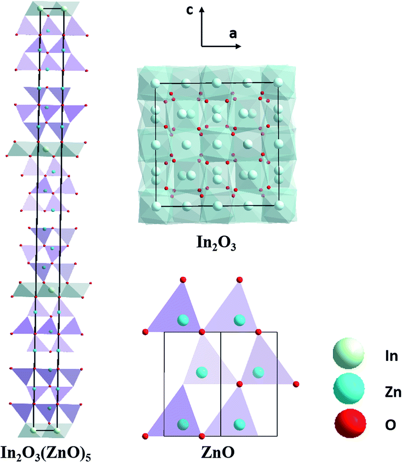
 33 (K is the Scherrer constant, d is the average thickness of the crystal grains perpendicular to the crystal plane direction, B is the diffraction width of the measured sample, θ is the diffraction angle, γ is the X-ray wavelength, 0.154056 nm).
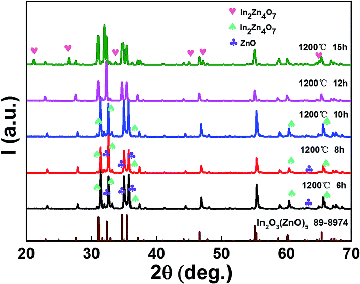


 is the Seebeck coefficient for a classical electron gas. The different holding times make different carrier concentrations of the samples. The temperature dependence of power factor (σα2) for In2O3(ZnO)5 (1200 °C for 6–15 h) bulks is shown in Fig. 4(c). The material has high figure of merit who has large power factor. All the samples showed a similar positive temperature dependence of σα2, despite having different slopes. With the increasing testing temperature, the power factor of the samples increased significantly because the Seebeck coefficient increased rapidly with temperature, and the power factor and the square of Seebeck coefficient were proportional. The maximum value of σα2 of 209 μW m−1 K−2 was acquired for In2O3(ZnO)5 (1200 °C, 8 h) at 973 K. In addition to In2O3(ZnO)5 (1200 °C, 15 h), the σα2 values of the specimens increased with increasing holding time.