
 Open Access Article
 This Open Access Article is licensed under a
 Creative Commons Attribution 3.0 Unported Licence
Screen printable MWCNT inks for printed electronics
Heera Menona,
Remadevi Aiswaryaab and
Kuzhichalil Peethambharan Surendran *ab
*ab
aMaterials Science and Technology Division, National Institute for Interdisciplinary Science and Technology (CSIR-NIIST), Thiruvananthapuram, India-695019. E-mail: kpsurendran@niist.res.in; Fax: +91 471 2491712; Tel: +91 471 2515258
bAcademy of Science and Innovative Research (AcSIR), New Delhi, India
First published on 11th September 2017
Abstract
Development of oxidation resistant conductive inks with low curing temperatures is a challenging problem in printed electronics. The present work introduces a newly formulated room temperature curable conducting ink using multiwalled carbon nanotubes (MWCNTs) for printable electronic application. The organic vehicle composition of the ink is meticulously controlled based on their rheological characteristics. The ink was screen printed on different flexible substrates like paper, Mylar®, photopaper, cellulose acetate sheets and silicone rubber. A morphological study of the printed pattern was also performed using SEM and AFM. The electrical characterization of the ink printed on flexible substrates was studied and a sheet resistance of 0.5–13 Ω sq−1 for three strokes was reported.
1. Introduction
The conductive ink industry has been booming to ever greater heights over the past few years.1 There are mainly two kinds of materials used for conductive inks: noble metal based (silver and copper)2–4 and carbon based materials (graphite and CNT).5,6 Each of these has their own defined features and advantages. In general, printable metals are either exorbitantly expensive (e.g. Au, Ag or Pt) or are subject to fast oxidation (e.g. Cu) which limit their wide usage in printed electronics.7 A promising addition to this list is the carbon nanotube (CNT), which is a lightweight inorganic structure with unique physical and electrical properties relative to traditional conductive materials.8In order to integrate carbon nanotubes in device fabrication, there are several techniques being used. Two of the major approaches adopted to deposit nanotubes at the selected areas of substrates are “grow in place” and “solution based printing” methods.9,10 Being an additive process, printing of CNT is considered as the simplest and cost effective method for transferring CNTs onto the substrate. Printed CNT coatings/thin films can be developed into solar cells, digital circuits,11 sensors12–14 and antennas.15 Printing of functional inks can be performed by numerous printing techniques like inkjet printing, flexographic printing, screen printing, roll to roll printing etc.7 Among all these techniques, screen printing is the most cost effective technique used where the ink poured on the partially masked screen is squeegeed to move across, resulting in its uniform transfer through the stencil openings, onto the substrate placed beneath it. Here, the alignment between the fabric screen mask and the substrate is rather easy compared to gravure printing, since the screen mask is semitransparent, and both the mask and the substrate are planar.
Developing a stable and screen printable ink using CNT has been a long time challenge, primarily due to the ink's prerequisites such as to possess a low viscosity at high shear rate and a fast viscosity recovery time.16,17 For achieving these requirements, the dispersion of the CNT and its flow characteristics through the screen mesh have to be strictly controlled. Besides, the stability of CNT suspension is difficult to achieve because of the nanotubes' inherent tendency to aggregate due to high Van der Waals attractions resulting in the formation of bundles or ropes. In 2009, Biswas et al. reported that highly stable CNT dispersions are possible by judiciously employing sodium dodecyl sulphate (SDS) and polyvinyl pyrrolidone (PVP) in the vehicle.18 As known, PVP is a polymer containing amide groups which can be cross-linked into a three-dimensional molecular network, and can act as a dispersant and binder at the same time. Furthermore, PVP being highly soluble in polar solvents like ethanol, phase separation could be avoided during the ink formulation. On the other hand, the dispersant, SDS has been known as an efficient dispersant for CNT dispersions in recent literature whose dispersion mechanism of CNT has been widely studied.19
In the present paper, we report the development and properties of a novel conductive MWCNT ink formulation that can be printed on different flexible substrates like Mylar®, cellulose acetate, photopaper and silicone rubber, with high degree of adhesion. The ink was formulated with proper rheological profile for higher throughput coatings using the flat-bed screen printing technique. The choice and proportion of organic contents were tricky enough so as to enable curing of the ink at room temperature. The microstructure, adhesion strength and electrical characteristics of the screen printed MWCNT patterns were also investigated.
2. Experimental
2.1 Materials
High purity pristine MWCNTs were purchased from Nanoshell Inc, USA. Anhydrous ethanol was purchased from Merck. Sodium dodecyl sulphate (99.9%) and polyvinyl pyrrolidone (MW 30,000) was procured from Sigma Aldrich.2.2 Instrumentation
The structure and microstructure of MWCNT and its printed patterns were analysed by scanning electron microscopy (JEOL-JSM 5600 LV, Tokyo, Japan), transmission electron microscopy (FEI Tecnai G2 30S-TWIN operated at 300 kV, FEI Company, Hillsboro, USA) and atomic force microscopy (Bruker Nano Inc., USA). The colloidal stability of the CNT ink was measured using a rheometer (Brookfield, R/S Plus, MA, USA). The adhesion test for printed pattern was done as per the ASTM standard (D 3359-97). The electrical properties of the printed patterns were measured using source meter by four probe method (Keithley 2450).2.3 Ink formulation and printing
An ink composition contains four elements: solvent, filler, dispersant and binder. Here an organic solvent based nanotube ink was formulated with ethanol as the solvent. For filler, commercially available multiwalled carbon nanotube (MWCNT, 99%, OD: <60 nm, length: 3–8 μm) was used as received without any further purification or treatment. To ensure proper dissolution of the mixture, the solubility of different dispersants and binder was checked prior to development of the ink. Finally, sodium dodecyl sulphate and polyvinyl pyrrolidone were chosen as the suitable dispersant and binder respectively for the ink formulation. The components of the ink such as SDS, PVP, ethanol and MWCNT have to be mixed thoroughly to form a stable homogeneous suspension. Generally used dispersion methods like bath and probe sonication were precluded since these methods would result in excessive evaporation of the solvent. Decisively, a controlled magnetic stirring technique was opted for blending the organic vehicle. The carbon nanotube ink preparation procedure begins with the addition of SDS into 5 ml ethanol. The dispersant was added prior to the filler in order to ensure proper suspension of the MWCNT and the dispersant loading was optimized as 7.5 wt% of filler loading. The MWCNT was added in to this mixture after 1 h of stirring which was followed by the addition of PVP after 2 h. The PVP loading was varied from 15 wt% to 50 wt% of CNT. The complete mixture was thoroughly stirred for the next 24 h.The MWCNT concentration in the ready-to-print ink was found to be about 9 wt% with respect to the total solvent content. The optimal concentration of the binder is required for proper adhesion of the ink to the substrate. Further, it can enhance the ink viscosity, debundle MWCNTs, stabilize the inks for a long time, and improve the printed device patterns. On the other hand, there should not be too much PVP in the inks which may result in very high viscosity and deteriorate the electrical conductivity.
The ink with optimal flow characteristics was screen printed on different flexible substrates like paper, Mylar®, photopaper, cellulose acetate sheet and silicone rubber using a semi-automatic screen printer (XPRT2, Ekra, Asys group, Germany). For printing, we used silk screens with mesh size 325 which is tightly bound over a metallic frame of dimension 220 × 220 mm.
3. Results and discussion
As mentioned before, MWCNTs consists of multiple rolled concentric graphene tubes which can be metallic or semiconducting. Fig. 1(a) and (b) represent TEM analysis of CNTs. It is observed that the CNTs we tested are multiwalled with diameter of the nanotubes ranging from 65–80 nm with lengths in micrometer range. The walls of the CNTs are distorted which may be attributed to the synthesis conditions. Fig. 1(a) represents a bamboo like CNT (BCNT). It is so called because nanotubes structure resembles the structure of bamboo. Here, the graphite layers are misaligned with the primary MWNTs axis. It is reported that bamboo defects consist of several transverse, internal walls segmenting the interior of a MWNT into independent pods or isolated volumes. Bamboo defects are often quasi-periodic and by nucleating new shells they maintain roughly constant outer diameters.20 As stated in the literature, as the diameter of the nanotube increases, metallic nature of the tube also predominates.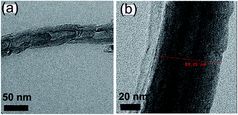 | ||
| Fig. 1 (a) and (b) shows TEM of multiwalled carbon nanotube. | ||
Rheological optimization of MWCNT ink is an important reliability criterion. Viscosity is a crucial parameter in optimizing the ink. Fig. 2 shows the viscosity studies of formulated MWCNT ink. For screen printing purpose the viscosity must be in the range of 1–10 Pa s which means the ink must neither be too loose nor too viscous. This is because loose ink will result in overflowing solvent, thus making it unprintable. On the other hand, if the ink is too viscous, then it would be difficult to spread it with the squeegee. As the amount of filler increases the viscosity tends to increase and vice versa.21,22 In other words, as more and more CNT is added, the ink becomes more concentrated and hence improves the viscosity. When the dispersant increases, it tends to disperse the CNT more uniformly, weakening the impact of agglomeration and thus decreasing the viscosity.
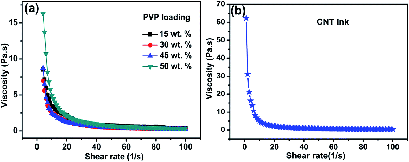 | ||
| Fig. 2 (a) Viscosity of CNT inks with 15, 30, 45 and 50 wt% PVP loading and (b) viscosity of the ready-to-print CNT ink. | ||
Fig. 2(a) represents the change in viscosity with increase in binder. In this work, the binder used was PVP. Here, this fluorine free polymer can act both as dispersant and binder, which can facilitate better dispersion of CNT bundles into a 3D continuous network. When the PVP weight loading is increased from 15 to 45 wt%, there is decrease in the viscosity. This is because it is the dispersion effect of PVP that dominates more in this case. But as the weight loading is increased to 50 wt%, there is an increase in viscosity implying that it starts behaving as a binder. The optimized concentration of PVP was observed to be 50 wt% with respect to filler loading. In Fig. 2(b), the final viscosity of the optimized ink is obtained as 2.09 Pa s. This ink possesses ideal flow characteristics suitable for screen printing.
The SEM analysis (Fig. 3) of the printed pattern was performed to understand the surface morphology and thickness of the printed pattern. Fig. 3(a) and (b) show uniformly distributed CNT networks as seen from the surface of the printed area. Here, the CNTs form connected networks which enhance the conducting nature of the printed pattern. It is signified from the images that the surface coverage is not due to the CNTs alone but a cluster of as grown CNTs and the binding material. Fig. 3(c) depicts the cross sectional view of the printed area which helps us to understand the thickness of the printed pattern. It was observed that the apparent thickness falls in the range 20–25 μm.
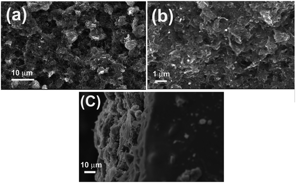 | ||
| Fig. 3 (a) and (b) shows surface morphology of printed CNT patterns, (c) describes the thickness of the CNT cross section. | ||
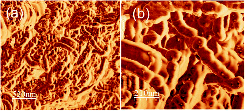
The RMS surface roughness quantifies the deviations from the mean surface, which helps to understand how the pattern appears to be, after the evaporation of the solvents. Atomic force microscopy was adopted to study the surface roughness of the printed pattern surface which is presented in Fig. 4. Different areas of the sample have been analysed and a couple of typical tapping mode micrographs are given in Fig. 4(a) and (b). The RMS surface roughness obtained was 64.4 nm, which is comparable to the roughness value reported in the literature.23 A more uniform surface would result in uniform sheet resistance, as the resistance is entirely depended on the connectivity of CNTs.
 | ||
| Fig. 4 (a) and (b) shows the optical images of printed patterns taken after the adhesion test. | ||
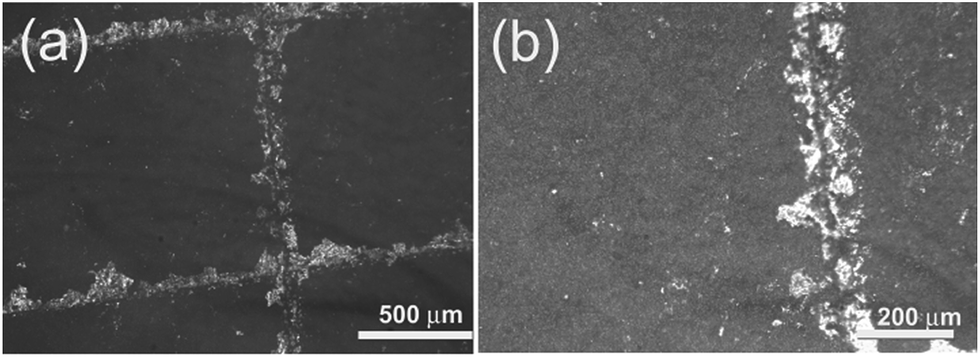
The adhesion test was done as per the ASTM standard (D 3359-97) and a few optical micrographs recorded after the test is shown in Fig. 5. Adhesion is one of the key properties that contribute to the electrical conductivity. For example, if the MWCNT networks are not adhered among themselves uniformly and to the surface of the substrate, it would result in poor electrical conductivity. Our adhesion test revealed that the adhesion was witnessed to be of Grade 4. In the present investigation, scotch™ tape was then used to detach some loosely bound MWCNTs. Conventional peel-off method to measure adhesion fails in carbon nanotube (CNT) film mainly due to ill-defined detached portions of the entangled CNTs. It was noted that small flakes of the coatings were detached from the surface which is less than 5% of the printed area as shown by the optical images in Fig. 5(a) and (b). Despite that, the overall peel off strength of the MWCNT coating on these substrates is well above the requirement for a high performance coating, which is ideal for flexible electronic applications against flexing as well as wear and tear.
 | ||
| Fig. 5 (a) and (b) AFM of printed MWCNT patterns taken at different magnifications. | ||
Fig. 6(a) shows the CNT patterns screen printed on Mylar® while Fig. 6(b) and (c) testifies the flexibility of printed substrate. Obviously, the flexibility is a necessary condition for practical device fabrication which demands for rollable and foldable devices. Fig. 6(d) shows the pattern printed on a typical photopaper.
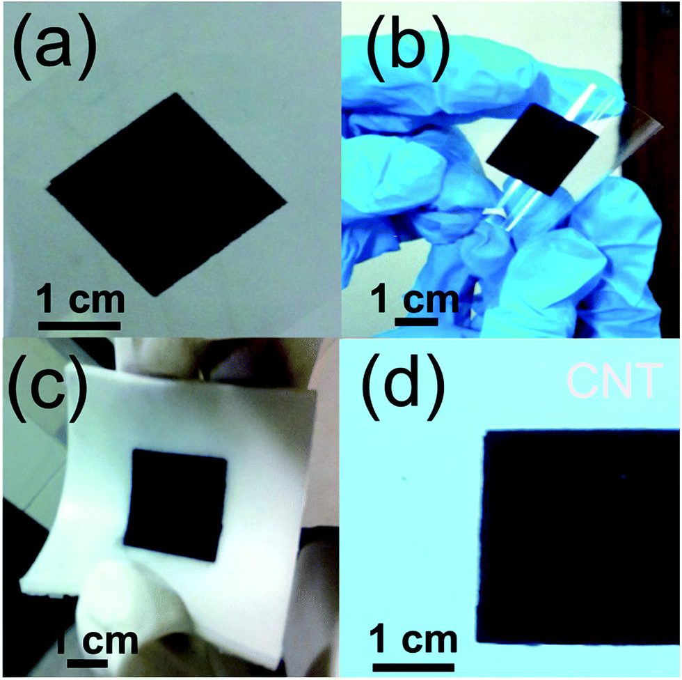 | ||
| Fig. 6 (a) CNT screen printed on Mylar®, (b) flexibility of screen printed CNT pattern, (c) CNT screen printed on silicone rubber and (d) CNT pattern screen printed on photopaper. | ||
Sheet resistance is another important parameter used to characterize a conducting ink. The sheet resistance of the printed pattern was measured using a four probe measurement set up and the I–V plot is as shown in Fig. 7(a). The sheet resistance was found to vary from sample to sample, depending on the connectivity of the CNT network. A well-connected CNT network of three strokes attained a sheet resistance of 0.5 Ω sq−1. At the same time, a sheet resistance of 13 Ω sq−1 was obtained in another three stroke printed sample which is believed to have an inferior network connection. The electrical conductivity of the printed pattern depends also on the adhesion of the CNT network to the substrate. A least adhered pattern would emanate in a highly resistive network. It was concluded that it would require higher weight loading of binder in order to print the ink on silicone rubber substrate for proper adhesion when compared to the other rough substrates like cellulose acetate, Mylar® and photopaper. The sheet resistance of the present ink was comparable with those reported in recent literature. Table 1 shows the comparison based on sheet resistance and printing method for other nanocarbon inks and silver based inks.
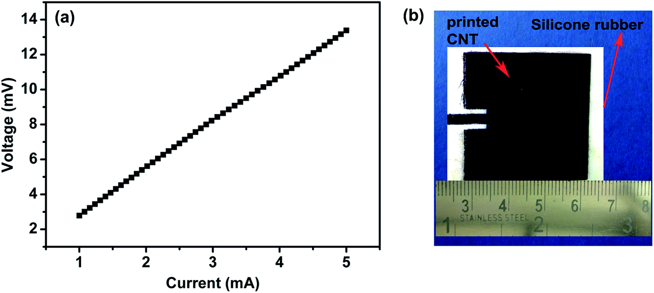 | ||
| Fig. 7 (a) I–V plot of printed CNT pattern, (b) CNT patch antenna pattern printed on silicone rubber substrate. | ||
| Ink | Printing method | Sheet resistance (conductivity) | Ref. | |
|---|---|---|---|---|
| 1 | SWCNT ink | Meyers rod | <1 Ω sq−1 (125 S cm−1) | 24 |
| 2 | SWCNT ink | Transfer and filtration method | 30 Ω sq−1 | 25 |
| 3 | SWCNT ink | Transfer printing | 200 Ω sq−1 | 26 |
| 4 | MWCNT ink | Flexographic printing | 0.12 to 3.00 kΩ sq−1 | 27 |
| 5 | SWCNT ink | Inkjet printing | 132 Ω sq−1 | 28 |
| 6 | SWCNT ink | Meyers rod | 10 Ω sq−1 | 29 |
| 7 | Silver ink | Inkjet printing | 38 Ω sq−1 | 30 |
| 8 | Copper foil | Commercial film | 0.001 Ω sq−1 | 31 |
| 9 | Silver ink | Screen printing | 50 mΩ sq−1 | 32 |
| 10 | Silver ink | Spray deposition | 50 Ω sq−1 | 33 |
| 11 | Silver ink | Screen printing | (4.67 × 10⁴ S cm−1) | 34 |
| 11 | Silver coating | Electroless deposition | 0.1 mΩ sq−1 | 35 |
| 12 | Silver ink | Direct write process | 1–10 Ω sq−1 | 36 |
| 13 | MWCNT ink | Screen printing | 0.5–13 Ω sq−1 | Present work |
The newly developed ink bypasses the high temperature curing, which is a pre-requisite for majority of the MWCNT based inks. Since the present formulation enables efficient 3D networked connected structure for MWCNT, it could offer improved electrical conductivity. This in turn, helps us to design facile development of conductive circuits employing MWCNT. As shown in Fig. 7(b), typical circuits like microwave patch antennas could be designed and screen printed using this facile methodology.
4. Conclusions
Development of novel conducting inks is a new direction in the field of printed electronics. Most of the commercial conductive inks available in the market are made of noble metals and requires stringent operating conditions to protect them from imminent oxidation. Furthermore, a majority of the inks require an annealing at temperature around 140 °C, in order to dispel away the high volatile vehicle holding the conductive filler particles, which is disadvantageous. Due to these reasons, the development of a room temperature curable ink, which does not suffer from oxidation problem, is a challenging task in flexible electronics. In the present work, a room temperature curable conducting MWCNT ink was formulated using suitable solvents, dispersants and binders. Here flatbed screen printing is the technique employed to print CNT ink on various flexible substrates like paper, Mylar®, cellulose acetate sheet and photopaper. Characterization of the CNT were done using TEM which indicated the presence of as grown MWCNT with distorted walls and many of them assume the structure of bamboo-like CNTs (BCNTs). The CNT ink printed on flexible substrates exhibited outstanding adhesion characteristics as per ASTM standard D3359-97 and sheet resistance in the range of 0.5–13 Ω sq−1 with minimum surface roughness (<65 nm).Conflicts of interest
There are no conflicts of interest to declare.Acknowledgements
The authors are grateful to Department of Science and Technology, New Delhi (SR/S2/CP-114/2012) for the financial support. One of the authors, R. Aiswarya, thanks Council of Scientific and Industrial Research, New Delhi for her research fellowship.References
- J. Perelaer, P. J. Smith, D. Mager, D. Soltman, S. K. Volkman, V. Subramanian, J. G. Korvink and U. S. Schubert, J. Mater. Chem., 2010, 20, 8446–8453 RSC.
- D. J. Finn, M. Lotya and J. N. Coleman, ACS Appl. Mater. Interfaces, 2015, 7, 9254–9261 CAS.
- W. J. Hyun, S. Lim, B. Y. Ahn, J. A. Lewis, C. D. Frisbie and L. F. Francis, ACS Appl. Mater. Interfaces, 2015, 7, 12619–12624 CAS.
- D. Li, D. Sutton, A. Burgess, D. Graham and P. D. Calvert, J. Mater. Chem., 2009, 19, 3719–3724 RSC.
- E. P. Randviir, D. A. Brownson, J. P. Metters, R. O. Kadara and C. E. Banks, Phys. Chem. Chem. Phys., 2014, 16, 4598–4611 RSC.
- E. B. Secor, S. Lim, H. Zhang, C. D. Frisbie, L. F. Francis and M. C. Hersam, Adv. Mater., 2014, 26, 4533–4538 CrossRef CAS PubMed.
- K. Suganuma, Introduction to printed electronics, Springer Science & Business Media, 2014 Search PubMed.
- M. F. De Volder, S. H. Tawfick, R. H. Baughman and A. J. Hart, Science, 2013, 339, 535–539 CrossRef CAS PubMed.
- N. Rouhi, D. Jain and P. J. Burke, IEEE Microw. Mag., 2010, 11, 72–80 CrossRef.
- N. Rouhi, D. Jain and P. J. Burke, ACS Nano, 2011, 5, 8471–8487 CrossRef CAS PubMed.
- M. Ha, Y. Xia, A. A. Green, W. Zhang, M. J. Renn, C. H. Kim, M. C. Hersam and C. D. Frisbie, ACS Nano, 2010, 4, 4388–4395 CrossRef CAS PubMed.
- I. Krucińska, E. Skrzetuska and W. Urbaniak-Domagała, Pulse, 2012, 11, 15 Search PubMed.
- H. Jing, Y. Jiang and X. Du, J. Mater. Sci.: Mater. Electron., 2012, 23, 1823–1829 CrossRef CAS.
- D. Janczak, G. Wróblewski, M. Jakubowska, M. Słoma and A. Młożniak, Challenges of Modern Technology, 2012, vol. 3, pp. 14–19 Search PubMed.
- Y.-M. Wu, X. Lv, B. K. Tay and H. Wang, 2013 International Conference on Optoelectronics and Microelectronics (ICOM), 7-9 Sept 2013, pp. 91–93 Search PubMed.
- Y. D. Lee, W.-S. Cho, S.-I. Moon, Y.-H. Lee, J. K. Kim, S. Nahm and B.-K. Ju, Chem. Phys. Lett., 2006, 433, 105–109 CrossRef CAS.
- D. R. Gamota, P. Brazis, K. Kalyanasundaram and J. Zhang, Printed organic and molecular electronics, Springer Science & Business Media, 2013 Search PubMed.
- C. Biswas, K. K. Kim, H.-Z. Geng, H. K. Park, S. C. Lim, S. J. Chae, S. M. Kim, Y. H. Lee, M. Nayhouse and M. Yun, J. Phys. Chem. C, 2009, 113, 10044–10051 CAS.
- W. H. Duan, Q. Wang and F. Collins, Chem. Sci., 2011, 2, 1407–1413 RSC.
- P. G. Collins, Defects and Disorders in Carbon Nanotubes, in Oxford Handbook of Nanoscience and Technology: Frontiers and Advances, ed. A. V. Narlikar and Y. Fu, Oxford University Press, Oxford, UK, 2009 Search PubMed.
- A. Pullanchiyodan and K. P. Surendran, Ind. Eng. Chem. Res., 2016, 55, 7108–7115 CrossRef CAS.
- A. M. Joseph, B. Nagendra, E. Bhoje Gowd and K. P. Surendran, ACS Omega, 2016, 1, 1220–1228 CrossRef CAS.
- M. Maksud, M. Yusof, Z. Embong, M. Nodin and N. Rejab, Int. J. Mater. Sci. Eng., 2014, 2, 49–55 Search PubMed.
- L. Hu and Y. Cui, Energy Environ. Sci., 2012, 5, 6423–6435 Search PubMed.
- Z. Wu, Z. Chen, X. Du, J. M. Logan, J. Sippel, M. Nikolou, K. Kamaras, J. R. Reynolds, D. B. Tanner and A. F. Hebard, Science, 2004, 305, 1273–1276 CrossRef CAS PubMed.
- M. W. Rowell, M. A. Topinka, M. D. McGehee, H.-J. Prall, G. Dennler, N. S. Sariciftci, L. Hu and G. Gruner, Appl. Phys. Lett., 2006, 88, 233506 CrossRef.
- T. Fischer, N. Wetzold, H. Elsner, L. Kroll and A. C. Hübler, Nanomater. Nanotechnol., 2011, 1, 3 CrossRef.
- R. P. Tortorich, E. Song and J.-W. Choi, J. Electrochem. Soc., 2014, 161, B3044–B3048 CrossRef CAS.
- L. Hu, J. W. Choi, Y. Yang, S. Jeong, F. La Mantia, L.-F. Cui and Y. Cui, Proc. Natl. Acad. Sci. U. S. A., 2009, 106, 21490–21494 CrossRef CAS PubMed.
- T. T. Nge, M. Nogi and K. Suganuma, J. Mater. Chem. C, 2013, 1, 5235–5243 RSC.
- J. Kim, B. Lee, J. Y. Lek, R. I. Made, B. Salam and C. L. Gan, Electronics Packaging Technology Conference (EPTC), IEEE 16th, 2014, pp. 27–30 Search PubMed.
- M. Hösel, R. R. Søndergaard, D. Angmo and F. C. Krebs, Adv. Eng. Mater., 2013, 15, 995–1001 CrossRef.
- V. Scardaci, R. Coull, P. E. Lyons, D. Rickard and J. N. Coleman, Small, 2011, 7, 2621–2628 CrossRef CAS PubMed.
- J. Liang, K. Tong and Q. Pei, Adv. Mater., 2016, 28, 5986–5996 CrossRef CAS PubMed.
- L. Lili, Y. Dan, W. Le and W. Wei, J. Appl. Polym. Sci., 2012, 124, 1912–1918 CrossRef CAS.
- S. Ghosh, R. Yang, M. Kaumeyer, C. A. Zorman, S. J. Rowan, P. X.-L. Feng and R. M. Sankaran, ACS Appl. Mater. Interfaces, 2014, 6, 3099–3104 CAS.
| This journal is © The Royal Society of Chemistry 2017 |