
 Open Access Article
 This Open Access Article is licensed under a
 Creative Commons Attribution 3.0 Unported Licence
Highly responsive photoconductance in a Sb2SeTe2 topological insulator nanosheet at room temperature
Shiu-Ming Huang *a,
Shih-Jhe Huanga,
You-Jhih Yanb,
Shih-Hsun Yub,
Mitch Choubc,
Hung-Wei Yangd,
Yu-Shin Changd and
Ruei-San Chend
*a,
Shih-Jhe Huanga,
You-Jhih Yanb,
Shih-Hsun Yub,
Mitch Choubc,
Hung-Wei Yangd,
Yu-Shin Changd and
Ruei-San Chend
aDepartment of Physics, National Sun Yat-Sen University, Kaohsiung 80424, Taiwan. E-mail: smhuang@mail.nsysu.edu.tw
bDepartment of Materials and Optoelectronic Science, National Sun Yat-Sen University, Kaohsiung 80424, Taiwan
cTaiwan Consortium of Emergent Crystalline Materials, TCECM, National Sun Yat-Sen University, Kaohsiung 80424, Taiwan
dGraduate Institute of Applied Science and Technology, National Taiwan University of Science and Technology, Taipei 10607, Taiwan
First published on 9th August 2017
Abstract
A photocurrent was applied to a Sb2SeTe2 topological insulator nanosheet at a wavelength of 325 nm, and it exhibited extremely high performance such that the responsivity and photoconductive gain are 354 A W−1 and 1531, respectively, at a bias of 0.1 V. This photoresponse is orders of magnitude higher than most reported values for topological insulators and two-dimensional transitional metal dichalcogenides. The photoresponse is linear with the applied voltage. Responsivity and gain under vacuum are higher than that in air by a factor of 2.5. This finding suggests that the Sb2SeTe2 topological insulator nanosheet has great potential for ultraviolet optoelectronic device applications.
I. Introduction
A system with a high surface area domain carrier and high carrier mobility is expected to be able to play a role in photodetecting applications. In addition to nanowires that possess a high surface-area-to-volume ratio, two-dimensional materials with high carrier mobility, such as graphene and graphene-based heterostructures, have attracted significant attention for their photoresponse-related application potential.1–3 However, their gapless structure and limited light absorption ratio prevent them from exhibiting efficient photocarrier separation or accumulation. This leads to poor performance in their photoresponsivity and photoconductive gain.1–4 To overcome this drawback, the integration of graphene and two-dimensional transitional metal dichalcogenides (TMDs) with a band gap appears to be a more promising approach.4–7 The reported results reveal that graphene–MoS2 and graphene–WSe2 hybrid structures have achieved extremely high performance in photoresponsivity and photoconductive gain.5–73D topological insulators are promising materials due to their insulating bulk state and gapless conducting surface state induced by the strong spin–orbit interaction.8,9 The insulating bulk state plays a role in photocarrier separation and accumulation. The linear dispersions in the surface state reveal an extremely high carrier mobility. This peculiar band structure in the topological insulator is similar to the proposed band structure in the graphene–MoS2 and graphene–WSe2 hybrid systems,5–7 and is expected to result in a high photoresponse. Several experimental works were performed on different topological insulators, which exhibited various kinds of characteristics that are expected to be able to be used in a wide range of applications.10–18 It has come to our attention that most photocurrent experiments have mainly focused on the application of visible and near infrared light to topological insulators, graphene–topological insulator heterostructures and 2D TMDs. Work with ultraviolet light is relatively rare, and the reported photocurrent performance is low.19–25
In this paper, we applied a photocurrent to a Sb2SeTe2 topological insulator at a wavelength of 325 nm. The experimental results show that the responsivity and photoconductive gain reached 354 A W−1 and 1531, respectively, at a bias of 0.1 V and a light intensity of 40 W m−2. These values are orders of magnitude larger than most reported values for topological insulators and 2D TMDs. It is therefore suggested that the Sb2SeTe2 nanosheet has great potential for future ultraviolet optoelectronic device applications.
II. Experimental method
Sb2SeTe2 single crystals were grown by a homemade resistance-heated floating zone furnace (RHFZ). The starting raw materials of Sb2SeTe2 were mixed according to the stoichiometric ratio. At first, the growth temperature was increased to 620 °C. The temperature was kept at 620 °C for 15 hours to let the raw material melt. The growth temperature was decreased from 620 °C to 580 °C at a rate of 1 °C h−1. Finally, the material was naturally cooled down to room temperature in an evacuated quartz glass tube. The material was used as a feeding rod for the following RHFZ experiment. After growth, the crystals were then furnace cooled to room temperature. The as-grown crystals were cleaved along the basal plane, with a silvery shining mirror-like surface, and then prepared for further experiments. The EDS and XPS spectra support the fact that the crystal is Sb2SeTe2.26The Sb2SeTe2 nanoflakes were obtained by exfoliating bulk crystals using dicing tape and were then dispersed on the insulating SiO2 (300 nm)/n-Si templates with pre-patterned Ti/Au circuits. Two platinum (Pt) metal contacts were subsequently deposited on the selected Sb2SeTe2 flakes using the focused-ion beam (FIB) technique. The thickness was about 181 nm and the surface area was approximately 1.18 μm2. As shown in Fig. 1, two Pt contacts were deposited on the sample for the photocurrent measurement. The current–voltage curve shows a linear dependence that supports the ohmic contacts in the sample. The conductivity is approximately 33.7 σ cm−1. Fig. 2 shows a schematic diagram of the nanosheet device illustrating the photoelectrical measurement setup and light illumination.
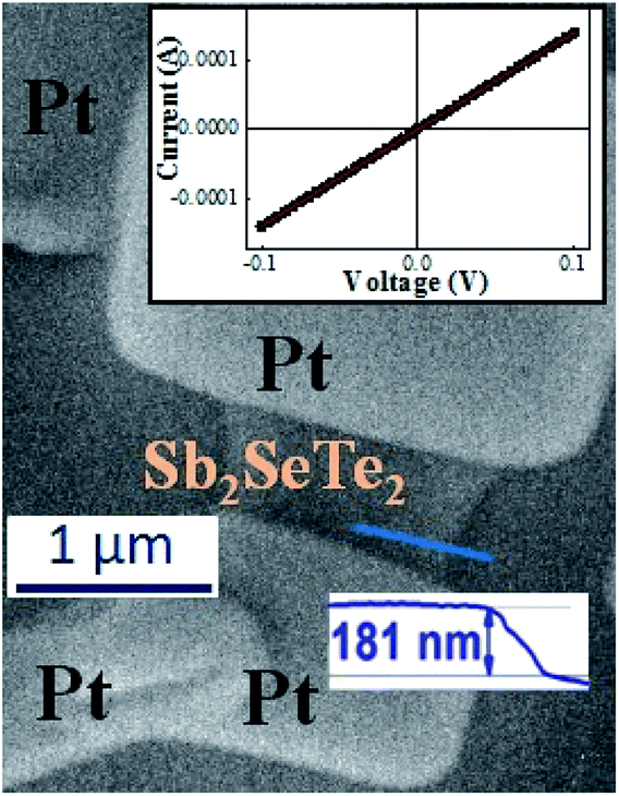 | ||
| Fig. 1 SEM picture of the Sb2SeTe2 nanosheet. Two Pt contacts are deposited on the nanosheet to measure the photocurrent. The top-right figure shows the linear current–voltage curve indicating the ohmic contact between the Pt electrodes and Sb2SeTe2 nanosheet. | ||
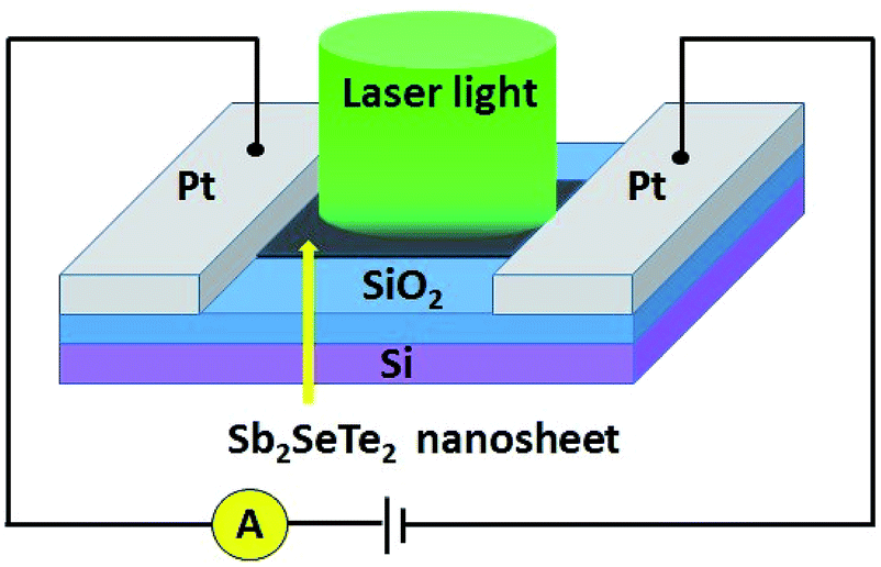 | ||
| Fig. 2 Schematic diagram of the nanosheet device illustrating the photoelectrical measurement setup and light illumination. | ||
A He–Cd UV laser with a wavelength of 325 nm was used as an excitation light source for the photoconductivity measurement. An optical diffuser was used to broaden the laser beam size (∼20 mm2) to uniformly illuminate the conduction channel of the nanosheets for the steady-state photocurrent measurements. The incident laser power was measured by a calibrated power meter (Ophir Nova II) with a silicon photodiode head (Ophir PD300-UV). The leakage current of the SiO2/Si template chip is of the order of 0.1 nA at a bias of 1 V. The leakage current is several orders of magnitude lower than the total measured current under UV light illumination.
III. Results and discussion
The inset of Fig. 3 shows the measured current of our Sb2SeTe2 nanosheet under light illumination with different powers of light. It clearly shows that the photocurrent increases with increasing light power. Fig. 3 shows the extracted photocurrent as a function of the light power intensity from 40 to 400 W m−2 at a bias of 0.1 V. To quantitatively analyze the relationship between the photocurrent and light intensity, the photocurrent was fitted by the simple power law relation, IP = APθ, where A is a constant for a certain wavelength, P is the power intensity of the light which is illuminated on the device, and θ is a constant that is related to the photosensitivity of the device. As shown in Fig. 3, the experimental data fits well with the power law relation, and the fitting result gives θ ≈ 0.82. This non-integer exponent can be regarded as a consequence of a complex process of electron–hole generation, trapping and recombination with the topological insulator.12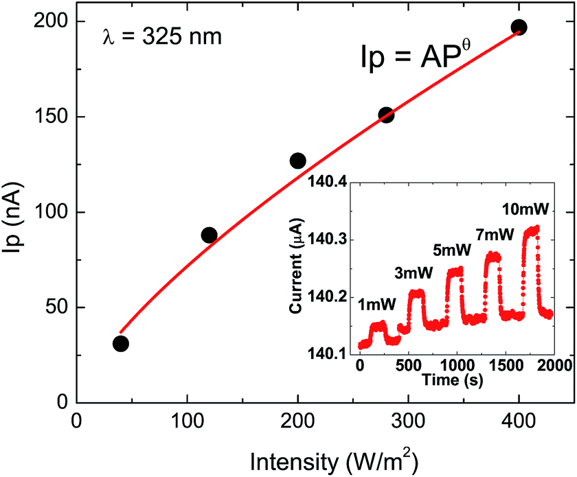 | ||
| Fig. 3 The measured photocurrent, as a function of light power intensity, which can be well described by the simple power law relation. The bottom-right inset shows the photocurrent at different powers of illuminating light. | ||
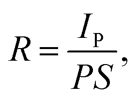
To quantitatively determine the performance of the Sb2SeTe2 nanosheet under light illumination, the responsivity, R, and the photoconductive gain, G, are calculated through the relation:
 | (1) |
 | (2) |
Fig. 4 shows the evaluated responsivity and photoconductive gain as a function of the light intensity at 0.1 V. It reveals that the responsivity and photoconductive gain decrease as the power intensity increases. The responsivity and photoconductive gain are 354 A W−1 and 1531 at a bias of 0.1 V and a power intensity of 40 W m−2. These values are among the largest reported values in the literature on topological insulators12,28–30 and 2D TMDs.31–41
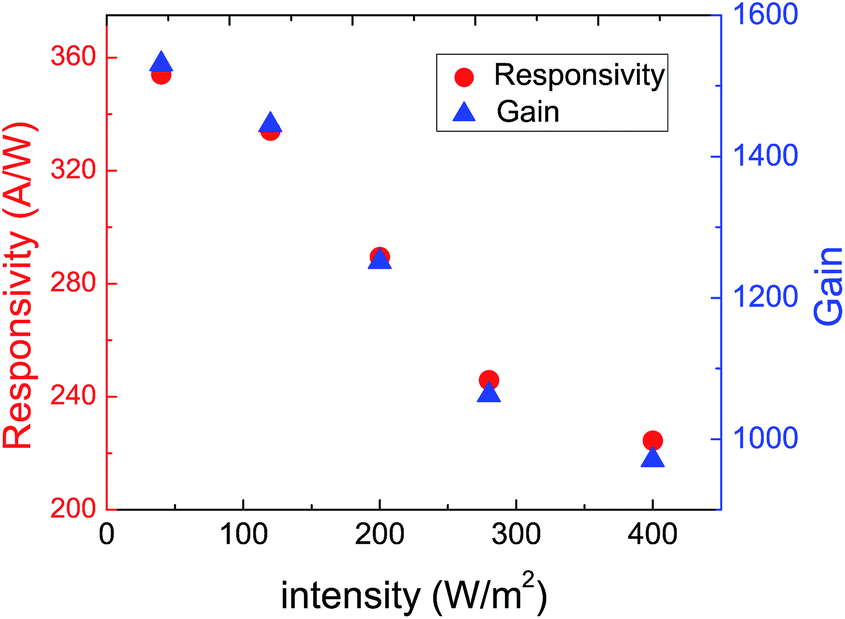 | ||
| Fig. 4 Responsivity and photoconductive gain as functions of the light power intensity at a wavelength of 325 nm. Both responsivity and photoconductive gain increase as the light power intensity decreases. | ||
There are several possible mechanisms that lead to the observed responsivity and gain in our Sb2SeTe2 topological insulator being several orders of magnitude higher than most reported values for topological insulators12,28–30 and 2D TMDs.31–41 Following the standard model, the photocurrent is directly related to the carrier transit time that might be expressed as τ = l2/μVsd, where τ is the carrier transit time, l is the device length, μ is the carrier mobility, and Vsd is the applied bias. The detected photocurrent is proportional to the carrier mobility and the applied bias.
An extremely high photoresponse has been observed in various kinds of graphene–TMD hybrid structures.5–7 The theoretical calculation reveals that the Dirac point lies within the gap of the bulk state,42 and our previous work supports the fact that the Fermi level lies below the Dirac point in our Sb2SeTe2 topological insulator.26,43 This band structure of the Sb2SeTe2 topological insulator is similar to the graphene–TMD hybrid structure. The energy of the light at 325 nm is much larger than the band gap of the bulk state; thus, the photons can easily generate electron–hole pairs. As shown in Fig. 5, the carriers in the valence band of the bulk state contribute to the conduction band of the bulk state through light assistance. The optic-induced carriers from the bulk state could partially contribute to the surface state with a linear dispersion band structure.25 Our previous work supports the fact that the surface state carrier mobility of our Sb2SeTe2 topological insulator is approximately 55.5 cm2 V−1 s−1.44
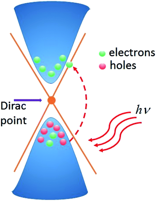 | ||
| Fig. 5 Schematic of the band structure. The carriers in the valence band of the bulk state contribute to the conduction band of the bulk state through light assistance. The optic-induced carriers from the bulk state could partially contribute to the surface state with a linear dispersion band structure. | ||
On the other hand, a topological insulator surface is quickly oxidized after it is exposed to the atmosphere. The surface condition strongly influences the carrier transport properties in low dimensional systems. The surface oxidation diminishes the topological insulator surface state and/or distorts the band structure. This surface oxidation reduces the effective carrier mobility. Our previous work revealed that the surface state carriers of our Sb2SeTe2 sheet are tolerant to surface oxidation that might come from unavoidable pollution during the fabrication process and experimental performance.26 This leads to less effective defective materials that would combine with the surface electron transport properties in our Sb2SeTe2 sheet.
Detectivity, which determines how weak irradiation can be distinguished from noise, is another important index used to characterize the performance of photodetectors. The specific detectivity (D*) is calculated through the relation:
 | (3) |
In addition to reducing the effective surface area, the adsorbed molecules on a topological insulator surface might create a local potential barrier that will bend the band structure and further influence the effective carrier mobility. The physical adsorbed molecules on the material’s surface would directly lower the effective light illumination area, carrier transition time and carrier mobility. In order to optimize the intrinsic optoelectronic characteristics of the Sb2SeTe2 nanosheet, the photocurrent was applied in bias-dependent and vacuum environments. Both the responsivity and gain are directly proportional to the photocurrent. As shown in Fig. 6, both the responsivity and gain were linear with the applied bias. Furthermore, both the responsivity and gain were enhanced under vacuum. Our experimental results show that both the responsivity and gain under vacuum were larger than those in atmospheric conditions by a factor of 2.5.
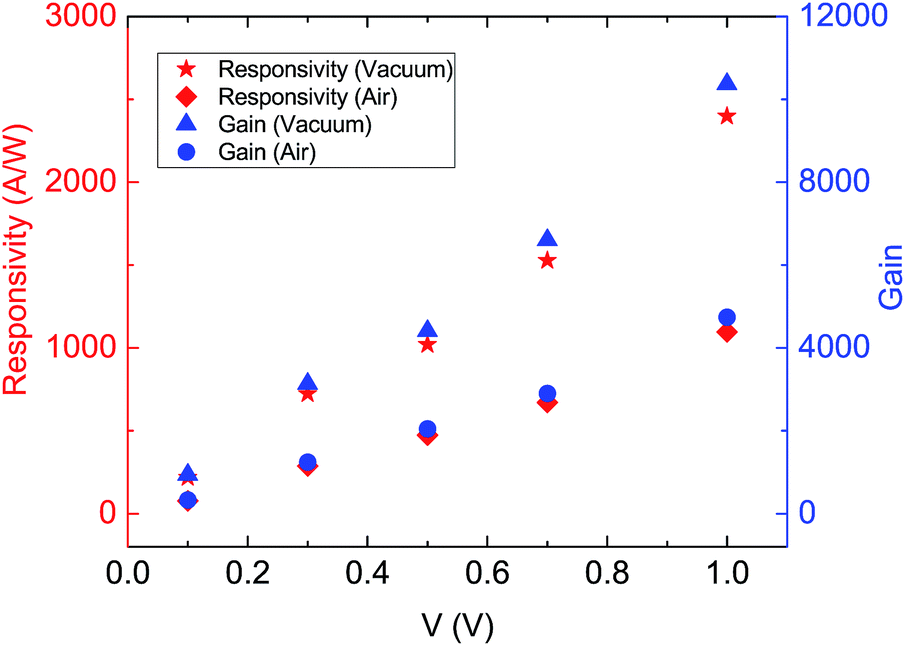 | ||
| Fig. 6 The responsivity and photoconductive gain are both linear with the applied bias in air and under vacuum. The responsivity and photoconductivity under vacuum are 2.5 times higher than in air. | ||
The responsivity versus wavelength (i.e. PC spectrum) measurement was conducted for the Sb2SeTe2 nanostructures. However, the intensity of the monochromatic light emitted from our monochrometer equipped with a Xe lamp light source is not high enough to generate a definable photoresponse, so we failed to get a successful PC spectrum. Nevertheless, to obtain information about the wavelength-dependent photoresponse, we conducted the photoresponse measurement using lasers as the light source. The light intensities for the different wavelengths were all controlled at the same value of 10 W m−2 and the photocurrents were normalized using the value at 325 nm. The result shows that the Sb2SeTe2 nanostructure has a better response to UV light than visible light. To see the responsivity ratio of UV light to visible light, responsivity values are also normalized using the value at 325 nm. The ratios of R(532 nm)/R(325 nm) and R(633 nm)/R(325 nm) are 82% and 58%, respectively.
IV. Conclusion
A photocurrent was applied to a Sb2SeTe2 topological insulator nanosheet at a wavelength of 325 nm. It exhibited extremely high performance, and the responsivity and photoconductive gain were 354 A W−1 and 1531, respectively, at a bias of 0.1 V. This high photoresponse is orders of magnitude higher than most of the reported values for topological insulators and 2D TMDs. The photoresponse is linear with the applied voltage. The responsivity and gain under vacuum are 2.5 times higher than those in air. This finding suggests that the Sb2SeTe2 topological insulator nanosheet has great potential for ultraviolet optoelectronic device applications.Acknowledgements
The work was supported by the Ministry of Science and Technology, Taiwan through Grant No. MOST 103-2112-M-110-009-MY3 and 106-2112-M-110-002, NSYSU-KMU co-operation project No. 103-I 008. for SMH, and Grant No. MOST 105-2112-M-011-001-MY3 for RSC.References
- F. Xia, T. Mueller, Y. M. Lin, A. Valdes-Garcia and P. Avouris, Ultrafast graphene photodetector, Nat. Nanotechnol., 2009, 4, 839–843 CrossRef CAS PubMed.
- T. Mueller, F. Xia and P. Avouris, Graphene photodetectors for high-speed optical communications, Nat. Photonics, 2010, 4, 297–301 CrossRef CAS.
- Y. Zhang, T. Liu, B. Meng, X. Li, G. Liang, X. Hu and Q. J. Wang, Broadband high photoresponse from pure monolayer graphene photodetector, Nat. Commun., 2013, 4, 1811 CrossRef PubMed.
- H. Qiao, J. Yuan, Z. Q. Xu, C. Y. Chen, S. H. Lin, Y. S. Wang, J. C. Song, Y. Liu, Q. Khan and H. Y. Hoh, et al., Broadband Photodetectors Based on Graphene VBi2Te3 Heterostructure, ACS Nano, 2015, 9, 1886–1894 CrossRef CAS PubMed.
- K. Roy, M. Padmanabhan, S. Goswami, T. P. Sai, G. Ramalingam, S. Raghavan and A. Ghosh, Graphene VMoS2 hybrid structures for multifunctional photoresponsive memory devices, Nat. Nanotechnol., 2013, 8, 826–830 CrossRef CAS PubMed.
- W. J. Yu, Y. Liu, H. Zhou, A. Yin, Z. Li, Y. Huang and X. Duan, Highly efficient gate-tunable photocurrent generation in vertical heterostructures of layered materials, Nat. Nanotechnol., 2013, 8, 952–958 CrossRef CAS PubMed.
- W. Zhang, C. P. Chuu, J. K. Huang, C. H. Chen, M. L. Tsai, Y. H. Chang, C. T. Liang, Y. Z. Chen, Y. L. Chueh and J. H. He, et al., Ultrahigh-Gain Photodetectors Based on Atomically Thin Graphene–MoS2 Heterostructures, Sci. Rep., 2014, 4, 3826 CrossRef PubMed.
- M. Z. Hasan and C. L. Kane, Topological insulators, Rev. Mod. Phys., 2010, 82, 3045 CrossRef CAS.
- X.-L. Qi and S.-C. Zhang, Topological insulators and superconductors, Rev. Mod. Phys., 2011, 83, 1057 CrossRef CAS.
- H. B. Zhang, J. D. Yao, J. M. Shao, H. Li, S. W. Li, D. H. Bao, C. X. Wang and G. W. Yang, Anomalous photoelectric effect of a polycrystalline topological insulator film, Sci. Rep., 2014, 4, 5876 CrossRef CAS PubMed.
- H. Qiao, J. Yuan, Z. Q. Xu, C. Y. Chen, S. H. Lin, Y. S. Wang, J. C. Song, Y. Liu, Q. Khan and H. Y. Hoh, et al., Broadband photodetectors based on graphene–Bi2Te3 heterostructure, ACS Nano, 2015, 9, 1886–1894 CrossRef CAS PubMed.
- K. Zheng, L. B. Luo, T. F. Zhang, Y. H. Liu, Y. Q. Yu, R. Lu, H. L. Qiu, Z. J. Li and J. C. Huang, Andrew. Optoelectronic characteristics of a near infrared light photodetector based on a topological insulator Sb2Te3 film, J. Mater. Chem. C, 2015, 3, 9154–9160 RSC.
- R. Huang, J. Zhang, F. F. Wei, L. Shi, T. Kong and G. S. Cheng, Ultrahigh Responsivity of Ternary SbVBiVSe Nanowire Photodetectors, Adv. Funct. Mater., 2014, 24, 3581–3586 CrossRef CAS.
- S. M. Huang, Y. J. Yan, S. H. Yu and M. Chou, Thickness-dependent conductance in Sb2SeTe2 topological insulator nanosheets, Sci. Rep., 2017, 7, 1896 CrossRef PubMed.
- S. M. Huang, S. J. Huang, Y. J. Yan, S. H. Yu, M. Chou, H. W. Yang, Y. S. Chang and R. S. Chen, Extremely high-performance visible light photodetector in Sb2SeTe2 nanoflake, Sci. Rep., 2017, 7, 45413 CrossRef CAS PubMed.
- S. M. Huang, S. H. Yu and M. Chou, Two-carrier transport-induced extremely large magnetoresistance in high mobility Sb2Se3, J. Appl. Phys., 2017, 121, 015107 CrossRef.
- S. M. Huang, S. H. Yu and M. Chou, The large linear magnetoresistance in Sb2Se2Te single crystal with extremely low mobility, Mater. Res. Express, 2016, 3, 126101 CrossRef.
- S. M. Huang, S. H. Yu and M. Chou, The temperature dependence of the crossover magnetic field of linear magnetoresistance in the Cu0.1Bi2Se3, Mater. Res. Express, 2016, 3, 086103 CrossRef.
- B. Radisavljevic, A. Radenovic, J. Brivio, V. Giacometti and A. Kis, Single-layer MoS2 transistors, Nat. Nanotechnol., 2011, 6, 147–150 CrossRef CAS PubMed.
- J. D. Yao, J. M. Shao, Y. X. Wang, Z. Zhaob and G. W. Yang, Ultra-broadband and high response of the Bi2Te3VSi heterojunction and its application as a photodetector at room temperature in harsh working environments, Nanoscale, 2015, 7, 12535–12541 RSC.
- J. D. Yao, Z. Q. Zheng and G. W. Yang, Layered-material WS2/topological insulator Bi2Te3 heterostructure photodetector with ultrahigh responsivity in the range from 370 to 1550 nm, J. Mater. Chem. C, 2016, 4, 7831–7840 RSC.
- J. D. Yao, Z. Q. Zhang and G. W. Yang, Promoting Photosensitivity and Detectivity of the Bi/Si Heterojunction Photodetector by Inserting a WS2 Layer, ACS Appl. Mater. Interfaces, 2016, 8, 12915–21924 CAS.
- J. D. Yao, Z. Q. Zheng, J. M. Shao and G. W. Yang, Stable, highly-responsive and broadband photodetection based on large-area multilayered WS2 films grown by pulsed-laser deposition, Nanoscale, 2015, 7, 14974–14981 RSC.
- Z. Zhang, T. Zhang, J. Yao, Y. Zhang, J. Xu and G. Yang, Flexible, transparent and ultra-broadband photodetector based on large-area WSe2 film for wearable devices, Nanotechnology, 2016, 27, 225501 CrossRef PubMed.
- J. D. Yao, J. M. Shao and G. W. Yang, Ultra-broadband and high-responsive photodetectors based on bismuth film at room temperature, Sci. Rep., 2015, 5, 12320 CrossRef CAS PubMed.
- S. M. Huang, C. Y. Huang, S. J. Huang, C. Hsu, S. H. Yu, M. Chou, P. V. Wadekar, Q. Y. S. Chen and L. W. Tu, Observation of surface oxidation resistant Shubnikov-de Haas oscillations in Sb2SeTe2 topological insulator, J. Appl. Phys., 2017, 121, 054311 CrossRef.
- E. A. El-Sayad and G. B. Sakr, Effect of annealing temperature on the structural and optical properties of amorphous Sb2Te2Se thin films, Cryst. Res. Technol., 2005, 40, 1139–1145 CrossRef CAS.
- A. Sharma, B. Bhattacharyya, A. K. Srivastava, T. D. Senguttuvan and S. Husale, High performance broadband photodetector using fabricated nanowires of bismuth selenide, Sci. Rep., 2016, 6, 19138 CrossRef CAS PubMed.
- H. Zhang, J. D. Yao, J. M. Shao, H. Li, S. W. Li, D. H. Bao, C. X. Wang and G. W. Yang, Anomalous photoelectric effect of a polycrystalline topological insulator film, Sci. Rep., 2014, 4, 5876 CrossRef CAS PubMed.
- C. Zang, X. Qi, L. Ren, G. L. Hao, Y. D. Liu, J. Li and J. X. Zhong, Photoresponse properties of ultrathin Bi2Se3 nanosheets synthesized by hydrothermal intercalation and exfoliation route, Appl. Surf. Sci., 2014, 316, 341–347 CrossRef CAS.
- P. A. Hu, Z. Z. Wen, L. F. Wang, P. H. Tan and K. Xiao, Synthesis of Few-Layer GaSe Nanosheets for High Performance Photodetectors, ACS Nano, 2012, 6, 5988–5994 CrossRef CAS PubMed.
- P. A. Hu, L. F. Wang, M. Yoon, J. Zhang, W. Feng, X. Wang, Z. Z. Wen, J. C. Idrobo, Y. Miyamoto, D. B. Geohegan and K. Xiao, Highly Responsive Ultrathin GaS Nanosheet Photodetectors on Rigid and Flexible Substrates, Nano Lett., 2013, 13, 1649–1654 CrossRef CAS PubMed.
- Z. Lin, H. Li, H. Li, L. Jiang, Y. Shi, Y. H. Sun, G. Lu, Q. Zhang, X. D. Chen and H. Zhang, Single-Layer MoS2 Phototransistors, ACS Nano, 2012, 6, 74–80 CrossRef PubMed.
- M. M. Furchi, D. K. Polyushkin, A. Pospischil and T. Muller, Mechanisms of Photoconductivity in Atomically Thin MoS2, ACS Nano, 2014, 14, 6165–6170 CAS.
- D. S. Tsai, K. K. Liu, D. H. Lien, M. L. Tsai, C. F. Kang, C. A. Lin, L. J. Li and J. H. He, Few-Layer MoS2 with High Broadband Photogain and Fast Optical Switching for Use in Harsh Environments, ACS Nano, 2013, 7, 3905–3911 CrossRef CAS PubMed.
- W. Zhang, J. K. Huang, C. H. Chen, Y. H. Chang, Y. J. Cheng and L. J. Li, High-gain phototransistors based on a CVD MoS2 monolayer, Adv. Mater., 2013, 25, 3456–3461 CrossRef CAS PubMed.
- H. S. Lee, S. W. Min, Y. G. Chang, M. K. Park, T. Nam, H. Kim, J. H. Kim, S. Ryu and S. Im, MoS2 Nanosheet Phototransistors with Thickness-Modulated Optical Energy Gap, Nano Lett., 2012, 12, 3695–3700 CrossRef CAS PubMed.
- W. Choi, M. Y. Cho, A. Konar, J. H. Lee, G. B. Cha, S. C. Hong, S. Kim, J. Y. Kim, D. Jena and J. Joo, et al., High-Detectivity Multilayer MoS2 Phototransistors with Spectral Response from Ultraviolet to Infrared, Adv. Mater., 2012, 24, 5832–5836 CrossRef CAS PubMed.
- D. H. Kang, M. S. Kim, J. Shim, J. Jeon, H. Y. Park, W. S. Jung, H. Y. Yu, C. H. Pang, S. J. Lee and J. H. Park, High-Performance Transition Metal Dichalcogenide Photodetectors Enhanced by Self-Assembled Monolayer Doping, Adv. Mater., 2015, 25, 4219–4227 CAS.
- R. B. Jacobs-Gedrim, M. Shanmugam, N. Jain, C. A. Durcan, M. T. Murphy, T. M. Murray, R. J. Matyi, R. L. Moore II and B. Yu, Extraordinary Photoresponse in Two-Dimensional In2Se3 Nanosheets, ACS Nano, 2014, 8, 514–521 CrossRef CAS PubMed.
- Z. Chen, J. Biscaras and A. Shukla, A high performance graphene/few-layer InSe photo-detector, Nanoscale, 2015, 7, 5981–5986 RSC.
- H. Lin, T. Das, L. A. Wray, S. Y. Xu, M. Z. Hasan and A. Bansil, An isolated Dirac cone on the surface of ternary tetradymite-like topological insulators, New J. Phys., 2011, 13, 095005 CrossRef.
- C. K. Lee, C. M. Cheng, S. C. Weng, W. C. Chen, K. D. Tsuei, S. H. Yu, M. M. C. Chou, C. W. Chang, L. W. Tu and H. D. Yang, et al., Robustness of a Topologically Protected Surface State in a Sb2Te2Se Single Crystal, Sci. Rep., 2016, 6, 36538 CrossRef CAS PubMed.
- S. M. Huang, S. H. Yu and M. Chou, Observation of surface oxidation resistant Shubnikov-de Haas oscillations in Sb2SeTe2 topological insulator, J. Appl. Phys., 2016, 119, 245110 CrossRef.
| This journal is © The Royal Society of Chemistry 2017 |