 Open Access Article
Creative Commons Attribution 3.0 Unported Licence
Fabrication of a spontaneously bent ZnO nanowire with asymmetrical dots by UV irradiation
Xinxin Wang†
 ab,
Zhipeng Li†a,
Xin Cao†a,
Zhiwei Wang*a and
Zhou Li
 *a
*a
aBeijing Institute of Nanoenergy and Nanosystems, Chinese Academy of Sciences, National Center for Nanoscience and Technology (NCNST), 100083, P. R. China. E-mail: wangzhiwei@binn.cas.cn; zli@binn.cas.cn
bKey Laboratory of Radiopharmaceuticals, Ministry of Education, College of Chemistry, Beijing Normal University, 100873, P. R. China
First published on 2nd August 2017
Abstract
We synthesised a spontaneously bent ZnO nanowire which has asymmetrical dots on its edge by UV irradiation. The bending angle increased with the extension of UV irradiation time. A further structure investigation revealed that this phenomenon was caused by an inhomogeneous crystallization process owing to UV localized heating.
As a wide band gap semiconductor with large excitation binding energy, zinc oxide (ZnO) has an extensive application in electronics as well as large scale optoelectronics. Its nanowire (NW) is a typical one-dimensional nanomaterial and has attracted more and more interest because of its various remarkable physical and chemical properties distinctive from conventional bulk materials. Many research groups have been actively involved in the study of both the synthesis and characteristics of ZnO NWs, which are widely applied to electronic devices,1 such as ultraviolet lasers,2 light-emitting diodes,3 solar cells,4 nanosensors,5 nanogenerators6 etc.
Some mature preparation methods of ZnO NWs provide feasibility for the end application.7 In previous studies, even if wires are of different sizes, most of the monocrystalline ones are straight from a morphological point of view. Recently, along with the major progress on strain engineered semiconductor micro/nano structures, some researchers bent the NWs with external force and look forward to specific properties compared with a straight one. The studies of elastic–plastic behavior of nanowires are of technological importance, because the electronic properties of nanowires may be affected by perturbing the band structure or changing the Fermi energy owing to strains.8 Fu and the co-workers demonstrated that when ZnO wire was bent by external force, it could effectively drift excitons so that excitons could be tuned in semiconductors improving the ultraviolet photoresponse.9 Wang reported that by increasing the NW bending, the photocurrent under ultraviolet illumination dropped dramatically and the photoresponse time became shorter.10 The formation of a bending NW could point the way towards a new approach to the fabrication of quantum dots (QDs). Zhang and his co-workers published a growth process of tensile and compressive stress-induced asymmetrical ZnO QDs on a bent ZnO NW.11 They considered that it is helpful in controlling the fabrication of well-crystallized ZnO QDs, which have the potential to improve the luminescence properties of future light-emitting devices. Han's group demonstrated the strain plasticity of nanowires in situ,12 and a novel high-resolution transmission electron microscopy technique was used to observed lattice distortion12 and deformation13 at the bending nanowires. These above findings of bent ZnO NW could demonstrate a big progress of the development of semiconductor devices and sensors.9 In addition, a bent nanowire conjugated system may have significant potential to be applied in flexible electronics, such as wearable devices and implanted medical devices etc.
In our recent research, we noticed that ZnO NW could bent spontaneously by UV irradiation. This is a very simple method compared with chemical doping14 and the ion beam15 which could cause the NWs twist or bent permanently. It is very interesting because the characteristics of a bent ZnO NW could be different with a straight one. Here, we investigated the details of the spontaneously bent ZnO NW formation, and some asymmetrical dots were formed on the bending NWs. We consider that such ZnO NWs prepared by this simple, low energy and low cost method have significant potential to be applied in the sensors and semiconductor devices.
The ZnO nanowires were first synthesized via hydrothermal method. They were grown on carbon cloth substrate. For this purpose, a 1.5 × 1.5 cm2 commercial carbon cloth were rinsed in acetone and ethyl alcohol in an ultrasonic bath three times and dried in a drying oven. Next, the substrate was cleaned with oxygen ions in the plasma cleaner for 2 minutes. The crystal seed was immediately dripped on the substrate. After drying, the substrate was immersed in the reaction solution bottled in quartz conical flask. The reaction solution was composed of 5% ammonium hydroxide and 4% 500 mM zinc nitrate (Sigma-Aldrich). At the beginning of the NW growth, we irradiated the substrates with UV light for a series of time. The intensity of UV light was 9 W cm−2, and the irradiation time was set up for 1, 5, 10 minutes. After UV treatment, the conical flask was set up in a water bath at 80 °C for 4 hours during which time the conical flask were covered with tinfoil to avoid exposing to light. ZnO NWs obtained through this procedure on the substrates. They were named as NW_1, NW_5 and NW_10 for 1, 5 and 10 minutes, respectively. ZnO NW synthesized without UV irradiation was named NW_0, which was used to denote the control sample.
The crystalline structure of the ZnO NW was characterized by an X-ray diffraction (XRD, D/max2200PC) instrument with Cu Kα line of 0.154 nm under 40 kV, 40 mA, 6° min−1. A Field Emission Scanning Electron Microscope (FESEM, Hitachi, SU8020) and Transmission Electron Microscope (TEM, Tecnai T20) were used to investigate the morphology of the nanowires. The crystal lattice was characterized by High Resolution Transmission Electron Microscope (HRTEM, FEI, Tecnai G2 F20 S-TWIN TMP). The PL spectra was measured by Raman spectrometer (HORIBA, LabRAM HR Evolution) with He–Cd laser (excitation wavelength is 325 nm) at room temperature.
The nanowires were synthesized via hydrothermal method on the carbon cloth substrate. We irradiated the substrates with UV irradiation for a series of time at the beginning of the growth process. As the control, some NWs were fabricated in dark. The morphology images of NWs were observed by Scanning Electron Microscopy (SEM) (Fig. 1). In the case of NWs prepared without the irradiation of UV light, NW_0, the NWs were straight. For NW_1, NW_5 and NW_10, some of NWs bend with the treatment of UV light. The amount of the bending NWs was increased with the extension of the irradiation time (Fig. 1b–d).
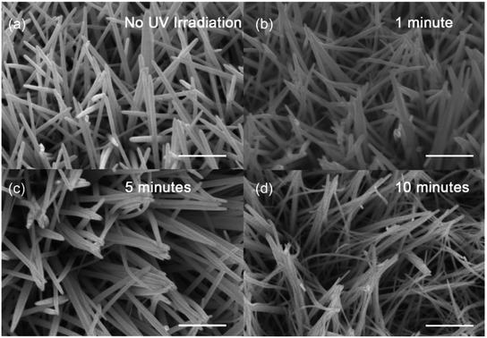 | ||
| Fig. 1 SEM images of the (a) NW_0, (b) NW_1, (c) NW_5 and (d) NW_10, respectively. The scale bar is 500 nm. | ||
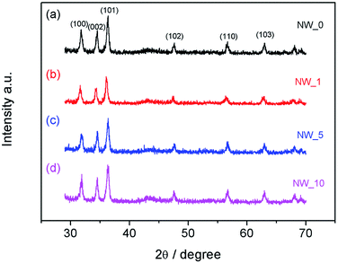
The crystallinity and crystal phase of the NWs described above was studied by XRD. Fig. 2 shows the typical WRD patterns for the ZnO NWs synthesized with or without the UV treatment. All the XRD results show a similar pattern, in that the ZnO NWs have high-purity wurtzite hexagonal phase. All of the diffraction peaks match well with standard hexagonal ZnO (JCPDS 36-1451). The peak intensity of (101) is stronger than others. In addition, the intensities of (002) and (100) peaks are also strong, which reveals that the NWs are well crystallized.
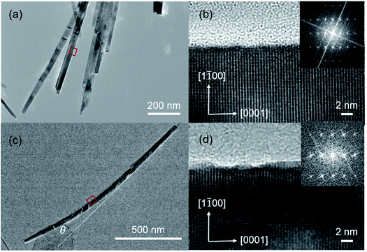
Transmission Electron Microscopy (TEM) operated at 200 kV with field emission gun was employed to investigate the microstructure of ZnO NWs. The ZnO NWs were scratched from substrate and then dispersed in ethanol. The suspended nanowires are lifted on a carbon coated TEM grid by dipping the grid in the solution. The grid is dried on a filter paper under an infrared lamp, followed by TEM characterization. In Fig. 3a and b, it is clearly observed that the ZnO NW synthesized without UV irradiation is straight and well crystallized with atomically smooth surface. The lattice constant along nanowire growth direction and the width direction is ∼0.52 nm and ∼0.28 nm, respectively, revealing that ZnO NW grew along [0001] direction. Fig. 3c shows that NW_10 NWs growing with UV irradiation are curved. Two lines parallel with the direction of nanowire growth were drawn in Fig. 3c to illustrate the bending angle of NWs (the bending angle of NW is defined as θ, which is the angle formed by two tangents). In the NW_10, this bending angle is ∼18.8 degrees. The surface of bending area is enlarged as demonstrated in Fig. 3d, showing rough surface with dots at nanometer-scale.
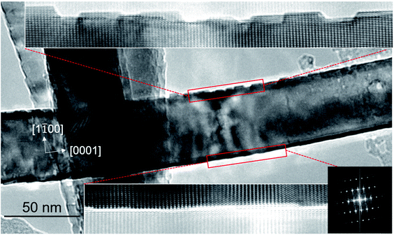
Fig. 4 shows the HRTEM images of surfaces of a bent nanowire for detailed microstructural analysis. The top surface (inner side of nanowire bending) has an aggregation of nanoscale dots with height of ∼1.8 nm and average width of ∼5.1 nm, while the bottom surface has much less dots. The bottom surface is smooth and the distribution of dots can be neglected. The lattice strain induced by nanowire bending is characterized by the change of lattice constant along [0001] direction compared with the ZnO bulk materials. It is calculated that the level of strain is −1.9% (compressive strain) and 0.4% (tensile strain) at the top and bottom surface area, respectively. Wang and coworkers bent ZnO nanowire by mechanical force inside TEM and also observed surface dots which nucleate to release strain energy. They found the average height of surface dots reach ∼1.5 nm when the compressive strain level is around 2.2% which is comparable with our results. Nevertheless, the level of strain at the top and bottom surfaces is not equal. The phenomenon implies that the directional UV irradiation can induce asymmetric heating and then temperature gradient on a single nanowire, resulting in the uneven growth speed of ZnO and therefore bending of the nanowire. The gradual deformation of nanowire accumulates strain energy on nanowire. As a result, the nanowire is spontaneously bent, and the formation of surface dots is to release the strain energy. At the same time, UV irradiation may also generate point defects (interstitials/vacancies) inside nanowire, but they cannot be directly observed by the conventional TEM technique.
Photoluminescence (PL) spectra were carried out to investigate the dislocations caused by the lattice deformation in bending NWs (Fig. 5). The spectra show clear peaks near 380 nm, which could be assigned to the intrinsic peak of ZnO. While the wide peaks at 560 nm and relative weak peaks at 750 nm were observed, they were caused by the vacancies and interstitials of NWs. We integrated the area of characteristic peaks described above, and the ratio of integrated peak intensities was used to investigate the relative degree of defects, R, of NWs. R values were calculated using the equations, R1 = S1/S2 and R2 = S1/S3. Where, S1, S2 and S3 represent the area of the peak at 380 nm, 560 nm and 750 nm, respectively. The results were summarized in Fig. 5b. It clearly showed that the R value decreased with the extension of irradiation time, which implied more defects were generated in the order of NW_10, NW_5 and NW_1. According to the defect levels of ZnO16 and the photon energy equation:
| E = hf = hc/λ |
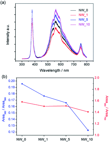 | ||
| Fig. 5 (a) Photoluminescence (PL) spectra of ZnO NWs and (b) the change of ratio of peak area at 380 nm to area at 560 nm (R1), and peak area at 380 nm to area at 750 nm (R2). | ||
Conclusions
In summary, we synthesised a spontaneously bent ZnO NW which had asymmetrical dots on its edge by UV irradiation. The bending degree of NWs was increased by the irradiation time. We considered that this phenomenon was caused by an accumulation of local strain owing to inhomogeneous crystallization process during nanowire growth by localized asymmetric heating of UV irradiation. The interstitial and vacancies of O inside nanowire were elucidated by photoluminescence spectra. The spontaneously bent ZnO nanowire could be fabricated by the UV irradiation. This bent nanowire has asymmetrical dots on its edge. This synthesis process with UV irradiation may introduce distinctive properties for NWs and it also may provide a new approach of providing spontaneously bent ZnO nanowire with asymmetrical dots for nanosensors and electric devices.Acknowledgements
This work was supported by the national key R & D project from Minister of Science and Technology, China (2016YFA0202703), National Natural Science Foundation of China (NSFC 31571006, 81601629 and 51603014), Beijing Talents Fund (2015000021223ZK21) and “Thousands Talents” program for pioneer researcher and his innovation team.Notes and references
- Y. W. Heo, D. P. Norton, L. C. Tien, Y. Kwon, B. S. Kang, F. Ren, S. J. Pearton and J. R. LaRoche, Mater. Sci. Eng., R, 2004, 47, 1 CrossRef.
- M. H. Huang, S. Mao, H. Feick, H. Q. Yan, Y. Y. Wu, H. Kind, E. Weber, R. Russo and P. D. Yang, Science, 2001, 292, 1897 CrossRef CAS PubMed.
- W. I. Park and G. C. Yi, Adv. Mater., 2004, 16, 87 CrossRef CAS.
- (a) J. B. Baxter and E. S. Aydil, Appl. Phys. Lett., 2005, 86, 1 CrossRef; (b) M. Law, L. E. Greene, J. C. Johnson, R. Saykally and P. D. Yang, Nat. Mater., 2005, 4, 455 CrossRef CAS PubMed.
- (a) T. Y. Wei, P. H. Yeh, S. Y. Lu and Z. L. Wang, J. Am. Chem. Soc., 2009, 131, 17690 CrossRef CAS PubMed; (b) P. H. Yeh, Z. Li and Z. L. Wang, Adv. Mater., 2009, 21, 4975 CrossRef CAS PubMed.
- (a) Z. L. Wang and J. H. Song, Science, 2006, 312, 242 CrossRef CAS PubMed; (b) X. D. Wang, J. H. Song, J. Liu and Z. L. Wang, Science, 2007, 316, 102 CrossRef CAS PubMed.
- (a) H. Gomez, S. Cantillana, F. A. Catano, H. Altamirano and A. Burgos, J. Chil. Chem. Soc., 2014, 59, 2447 CrossRef; (b) M. Taghavi, V. Mattoli, B. Mazzolai, C. Filippeschi and L. Beccai, Nanoscale, 2013, 5, 3505 RSC; (c) C. Min, X. Shen and W. Sheng, Appl. Phys. A: Mater. Sci. Process., 2009, 96, 799 CrossRef CAS; (d) H. Wan and H. E. Ruda, J. Mater. Sci.: Mater. Electron., 2010, 21, 1014 CrossRef CAS; (e) J. Elias, R. Tena-Zaera and C. Levy-Clement, J. Electroanal. Chem., 2008, 621, 171 CrossRef CAS.
- X. D. Han, K. Zheng, Y. F. Zhang, X. Zhang, Z. Zhang and Z. L. Wang, Adv. Mater., 2007, 19, 2112 CrossRef CAS.
- (a) X. W. Fu, G. Jacopin, M. Shahmohammadi, R. Liu, M. Benameur, J. D. Ganiere, J. Feng, W. L. Guo, Z. M. Liao, B. Deveaud and D. P. Yu, ACS Nano, 2014, 8, 3412 CrossRef CAS PubMed; (b) X. W. Fu, Z. M. Liao, J. Xu, X. S. Wu, W. L. Guo and D. P. Yu, Nanoscale, 2013, 5, 916 RSC.
- P. Gao, Z. Z. Wang, K. H. Liu, Z. Xu, W. L. Wang, X. D. Bai and E. G. Wang, J. Mater. Chem., 2009, 19, 1002 RSC.
- L. H. Wang, X. D. Han, Y. F. Zhang, K. Zheng, P. Liu and Z. Zhang, Acta Mater., 2011, 59, 651 CrossRef CAS.
- (a) Y. F. Zhang, X. D. Han, K. Zheng, Z. Zhang, X. Zhang, J. Y. Fu, Y. Ji, Y. J. Hao, X. Y. Guo and Z. L. Wang, Adv. Funct. Mater., 2007, 17, 3435 CrossRef CAS; (b) X. D. Han, Y. F. Zhang, K. Zheng, X. N. Zhang, Z. Zhang, Y. J. Hao, X. Y. Guo, J. Yuan and Z. L. Wang, Nano Lett., 2007, 7, 472 CrossRef PubMed.
- L. H. Wang, P. Liu, P. F. Guan, M. J. Yang, J. L. Sun, Y. Q. Cheng, A. Hirata, Z. Zhang, E. Ma, M. W. Chen and X. D. Han, Nat. Commun., 2013, 4, 2413 Search PubMed.
- R. N. Gayen, S. N. Das, S. Dalui, R. Bhar and A. K. Pal, J. Cryst. Growth, 2008, 310, 4073 CrossRef CAS.
- C. Borschel, S. Spindler, D. Lerose, A. Bochmann, S. H. Christiansen, S. Nietzsche, M. Oertel and C. Ronning, Nanotechnology, 2011, 22, 18 CrossRef PubMed.
- B. X. Lin, Z. X. Fu and Y. B. Jia, Appl. Phys. Lett., 2001, 79, 943 CrossRef CAS.
Footnote |
| † These authors contributed equally to this work. |
| This journal is © The Royal Society of Chemistry 2017 |

