
 Open Access Article
 This Open Access Article is licensed under a Creative Commons Attribution-Non Commercial 3.0 Unported Licence
Origin of surface potential in undoped zinc oxide films revealed by advanced scanning probe microscopy techniques
Ting Su *
*
State Key Laboratory of Surface Physics, Department of Physics, Fudan University, Shanghai 200433, China. E-mail: 14110190063@fudan.edu.cn
First published on 1st September 2017
Abstract
This paper presents recent studies combining piezoresponse force microscopy and Kelvin probe force microscopy to reveal the origin of bias-induced changes of surface potential in undoped zinc oxide (ZnO) films at the nanoscale. Surface potential under dc bias in ZnO films is studied using Kelvin probe force microscopy (KPFM). In addition, the piezoelectric properties of the ZnO are investigated by applying voltage using piezoresponse force microscopy (PFM), which is adopted to provide new physical insight into the important role of polarization charge in surface potential. PFM and KPFM results suggest that the origin of surface potential under an electric field in undoped ZnO film is determined by polarization charge, injection charge and surface charge. In addition, significant change in the Fermi level (work function) of undoped ZnO is found by positive (negative) biasing. The qualitative and quantitative study of surface potential and charge trapping properties can be useful for designing advanced nanoscale nonvolatile memory devices.
1. Introduction
Zinc oxide (ZnO) has unique electrical, piezoelectric, optical, and ferroelectric-like properties. ZnO is attracting an increasing level of interest as a direct-band-gap semiconductor for its functional applications. Reprogrammable nonvolatile memory represents an essential element in most modern electronic devices.1 ZnO is a promising material for nonvolatile random-access-memory applications1 because it can provide high performance as well as low power consumption, high environmental stability, and optical transparency. The arrangement of the dipoles2 and switching features significantly influence macroscopic properties. However, the nanoscale behavior of the ZnO is not sufficiently understood to make full use of this material.At the nanometer scale, microscopy3–5 techniques have become primary tool for studying surface topography, structure and electronic, mechanical, optical and transport properties. Piezoresponse Force Microscopy (PFM) and Kelvin Probe Force Microscopy (KPFM) is widely used due to good spatial resolution and easy manipulation for polarization.6–8 PFM provides additional important information on polarization through local piezoresponse.7 When dc bias is applied to the ZnO sample, polarization switching occurs and screen charge7 is transferred to the surface. The polarization charges are of great significance for the origin of surface potential in undoped ZnO films. Understanding the surface potential under dc bias in the ZnO films is important for practical application. In addition, it is interesting to explore how charge trapping effect and polarization charge constitute surface potential.8 It has been reported the correlation between polarization charge and surface potential of ferroelectric materials by Kalinin and Kim et al.,6–8 while the publication on surface potential of polarized regions of the undoped ZnO film remains rare. A report that the surface potential of the zinc oxide film has been studied without external stimuli of electric filed.9
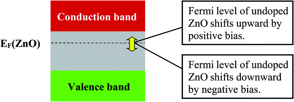
However, in previous work,9 polarization information can not be obtained. Polarization information is essential to getting new physical insight into the role of polarization charge in surface potential. To study the polarization switching, PFM should be adopted. Therefore, in this study, the origin of surface potential under dc bias in undoped ZnO was investigated by a combined use of PFM and KPFM. It is found polarization charge is key role in surface potential of undoped ZnO film. In addition, it is also found Fermi level of undoped ZnO shifts upward (downward) by positive (negative) bias. The study of trapped charges is promising for zinc oxide based nonvolatile memory application.
The article is organized as follows. In Section 2, material preparation and experimental techniques are described. In Section 3, we present the results and discussion of PFM and KPFM imaging of the undoped ZnO sample. The conclusion of the article is given in Section 4.
2. Experiment
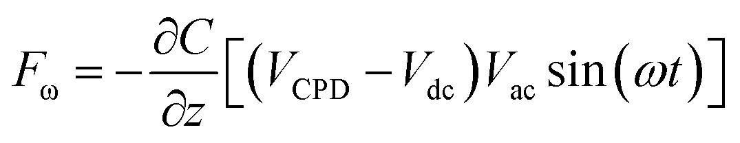
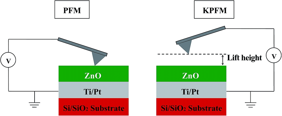
Pulsed laser deposition was adopted to prepare pure ZnO film on Si/SiO2/Ti/Pt substrate at 600 °C. Pt is used as bottom electrode. The thickness of the sample was measured to be 69 nm. In this work, the thickness of undoped ZnO thin film was measured by ellipsometry. The popular optical technique for studying the thickness of thin films is ellipsometry, which measures polarization change. Kelvin probe force microscopy is noncontact technique (Fig. 1) to study structural and electrical properties of surfaces and interfaces, and it can obtain nanoscale mapping of surface potential.10 KPFM technique exploits long-range electrostatic interactions between sample and tip. In KPFM measurements of conductive samples, tip-sample interaction is only due to Fermi level alignment, therefore, the local surface potential difference is simply related to the tip-sample work function difference.11,12 In order to minimize cross talk between the topography and electrostatic signal, two-pass technique is used in KPFM.13,14 In the first pass, topography information is recorded. In the second pass, the tip is lifted to a user-selected separation between sample surface and tip. In addition, several scanning parameters can be controlled in order to optimize the operating condition. KPFM experiments were carried out under an ac voltage of 3 V. The tip is kept a distance of 40 nm above the sample surface. These scanning parameters are equal to that of the previous work.9 A dc voltage Vdc and an ac voltage Vac![[thin space (1/6-em)]](https://www.rsc.org/images/entities/char_2009.gif) sin(ωt) are applied to the cantilever, with ω close to cantilever resonance frequency.10 The cantilever oscillated at frequency ω due to electrostatic force between tip and sample. The ω component of electrostatic force is given by
sin(ωt) are applied to the cantilever, with ω close to cantilever resonance frequency.10 The cantilever oscillated at frequency ω due to electrostatic force between tip and sample. The ω component of electrostatic force is given by
 | (1) |
 | ||
| Fig. 1 PFM operating in contact mode and KPFM operating in non-contact mode. | ||
Complementarily, piezoresponse force microscopy was used to provide additional important information about local polarization by recording electromechanical displacements.16 PFM works according to the reverse piezoelectricity principle, i.e. piezoelectric material will deform in accordance with the applied biases.17 PFM is a contact mode and practical technique for local nanoscale imaging, spectroscopy and manipulation of piezoelectric and ferroelectric materials. The PFM tip is brought into contact with the sample surface during the scan. Fig. 1 shows schematics of the PFM technique. Dual frequency resonance tracking technique18 (DART) was adopted in PFM to track the contact resonance. To improve signal-to-noise ratio and magnify the signal, dual excitation of the cantilever independently measures both the amplitude and resonance frequency of the cantilever. The PFM and KPFM measurements were conducted on a commercial SPM (MFP-3D, Asylum Research, USA). A Pt-coated tip (Electri-Lever, Olympus, Japan, with spring constant = 2 N m−1 and resonant frequency = 70 kHz, tip radius ∼15 nm) was used. The nature of tip such as its radius, stiffness and sharpness are of great importance to high-resolution SPM studies.13,19
3. Results and discussion
Surface potential of undoped ZnO film was measured before bias application. Fig. 2(a) and (b) show topography and surface potential images of the ZnO film respectively. The positive surface potential value suggests the formation of Schottky contact between the ZnO and metal tip. To explain observations about the metal/semiconductor interface, we consider Mott–Schottky model. Schottky junctions are characterized by Schottky barrier, depletion width and rectifying behavior. A depletion layer (diffusion layer) and band bending is formed. The KPFM results accurately explain electrical properties of the metal/semiconductor interface.20 When the ZnO sample and the Pt-coated tip are electronic contact, the difference in work function results in charging of the sample and the tip, leading to the contact potential difference. The value of the contact potential difference is 359 mV. KPFM is sensitive to the electric potential variations induced by charges locate both at the surface and in the interior of the film.21 The surface shown in Fig. 2(a) has roughness rms of 4.9 nm. It has been reported that novel stabilization mechanism on polar surface, which is important discovery.22,23 Furthermore, the study of manipulation of subsurface donors in ZnO provides interesting insight into the understanding of microscopic mechanism about memory effect.24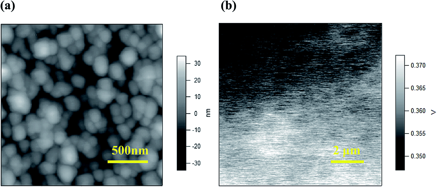 | ||
| Fig. 2 (a) Surface topography (b) surface potential image of undoped ZnO film before applying bias. | ||
The charge trapping properties of undoped ZnO film was investigated by studying surface potential under dc bias. A series of negative and positive dc biases, ranging from −3 to 0 V with a step 1 V and 0 to 10 V with a step 2 V, were applied to the undoped ZnO by contact mode, which procedure is similar to the previous report by Kim et al.6 Surface potential image obtained after bias application is shown in Fig. 3(a). In addition, the quantitative data of surface potential under dc bias is shown in Fig. 3(c). For the ZnO film, positive bias up to +10 V results in surface potential change of 56 mV. For the negative bias down to −3 V, surface potential change is −59 mV. Surface potential value of the ZnO film decreases with the applied negative bias and increases with the applied positive bias. To rationalize the phenomenon, we consider screening model25 for the surface–interface junction. After the poling process, screen charges including the charge from the air and injection charge significantly affect the surface potential. In the case of the surface potential under dc bias in ZnO film, screen charges and polarization charge contribute to surface potential. Major contribution to surface potential under dc bias in undoped ZnO film is polarization charge, injection charge and surface charge. Surface potential value can be influenced by the details of sample preparation and synthesis. In addition, it is found Fermi level of undoped ZnO film shifts upward (downward) by positive (negative) bias, as shown in Fig. 4. The Fermi level26 of a material is a fundamental quantity that determines its electronic properties. Fermi level position shifts suggest that the electronic structure of ZnO films change by applying voltage. It is also found ZnO film is capable of trapping both positive and negative charges, which is promising for nonvolatile memory applications. The charge trapping abilities of undoped ZnO films may be attributed to oxygen vacancy. Oxygen vacancies27 in ZnO are known to determine physical and chemical properties.
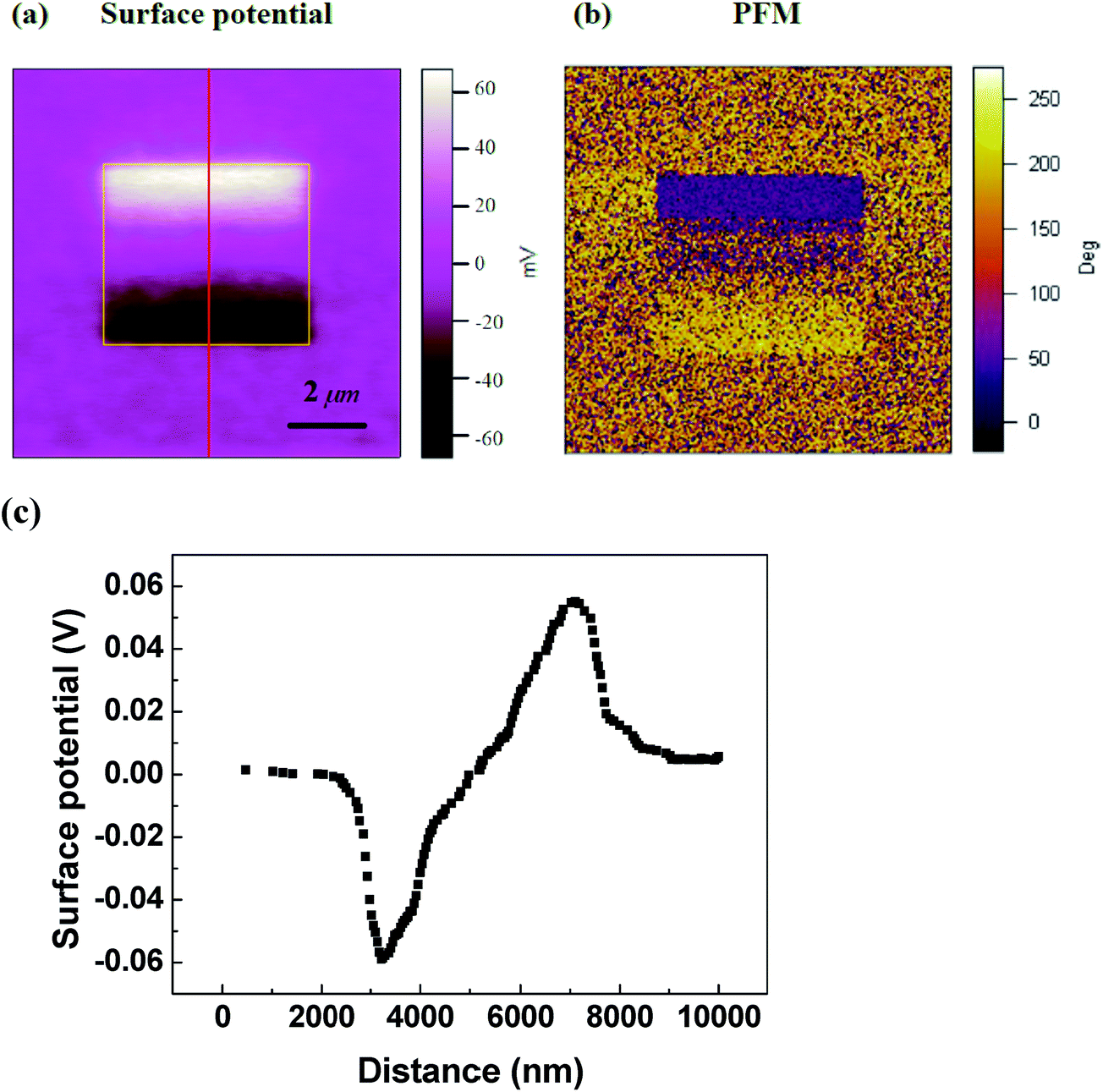 | ||
| Fig. 3 (a) Surface potential image of undoped ZnO film after applying bias. (b) PFM phase image scanned on the same region as the surface potential image. (c) KPFM data obtained from (a). | ||
 | ||
| Fig. 4 Schematic band diagram of the ZnO and it under positive/negative bias. | ||
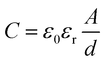
From surface potential data, surface charge density can be calculated by parallel capacitor model.2 The capacitance C between sample and tip is expressed as
 | (2) |
| Q = σA = CV | (3) |
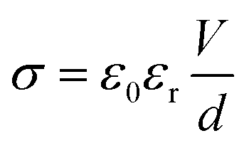
As a result, surface charge density σ can be obtained.2
 | (4) |
Taking the remnant polarization of 0.4 μC cm−2 and relative dielectric constant28 of 8.75. Therefore, surface charge density of undoped ZnO film is calculated to be 1.9 × 10³ to 6.5 × 10³ pC cm−2, suggesting that the overscreen ratio is about 1%.
Polarization switching in undoped ZnO was studied to provide novel perspective into the role of polarization charge in surface potential. Polarization switching under dc bias was studied by PFM on the same region as the KPFM image. PFM phase image after a series of dc biases is shown in Fig. 3(b). The orientation of dipoles in ZnO is aligned in both upward (yellow color) and downward direction (purple color). When positive voltage of +2 V is applied to the ZnO, partial polarization switching occurs and the nucleation of downward domain is observed. The partial polarization switching arises from the small bias to completely reverse the domains. It is important to understand the typical domain switching behavior. PFM is commonly believed to map the domain with the resolution of a few nanometers.29 The difference between PFM signals obtained from different domains on a multi-domain sample will be denoted by ‘PFM contrast’.29 PFM phase image provides information on polarization directions. In addition, the position of domain boundary can be determined by PFM measurements.29 Different domains are separated by domain boundary (domain wall).30 Therefore, it can be distinguished domains in the PFM images. Moreover, the domain size is 60 nm, which studied by PFM. New domain can nucleate and polarized domain can change their orientation due to external electric field.31 For the positive bias from +8 V to +10 V, the domain switching angle is 180° and complete switched domain was observed, suggesting downward polarization written in ZnO. For the negative bias, the PFM phase image show insignificant change after poling. It should be note that polarization switching may be related to defects, which act as pinning centers.32 The defect formation enthalpies33 in ZnO are small and the resulting oxygen vacancy influences the domain switching. ZnO has ferroelectric-like properties, which show the boundary between unpoled and poled areas. The clearly defined boundary was observed at the area with applied bias of +8 V and +10 V. In addition, as ZnO has strong piezoelectric response,34 mechanical stress could be generated by external electric filed.
The relationship between local polarization orientation and surface potential can be established by comparison of PFM and KPFM image from the same region.7 (Fig. 3(a) and (b)) PFM image of the ZnO film is compared to KPFM image obtained from the same area. The PFM and KPFM results indicate that polarization charge, injection charge and surface charge contribute to surface potential in undoped ZnO film. The polarization charges are attributed to rotation of the dipoles under dc bias.7 Moreover, the stability of trapped holes and electrons in undoped ZnO film was investigated by grounded tip scan, which discharge trapped surface charge. In order to study the role of trapped holes and electrons, discharging experiments were conducted. For the progress of discharging, contact mode scans with grounded tip were carried out for two times, which progress is similar to previous report by Kim et al.6 Fig. 5(a) and (b) show surface potential images of undoped ZnO after the first and second grounded tip scans. The value of surface potential change decreased after grounded tip scans. This observation may be due to the fact that surface charge was discharged.6 The PFM and KPFM results reveal that polarization charge, injection charge and surface charge are important for surface potential of undoped ZnO.
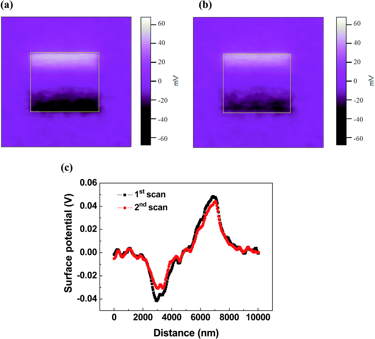 | ||
| Fig. 5 Surface potential images of undoped ZnO after (a) the first and (b) second grounded. Tip scan. (c) KPFM data obtained from (a) and (b). | ||
4. Conclusions
In conclusion, the surface potential of the piezoelectric domains of undoped ZnO film has been studied by a combined use of PFM and KPFM techniques. We clearly observe piezoelectric properties and surface potential change induced by external electric filed. PFM was adopted to get new information on the relationship between polarization charge and surface potential. We find that polarization charge, injection charge and surface charge play important role in origin of surface potential under dc bias in undoped ZnO film. In addition, Fermi level position of undoped ZnO film shifts by positive (negative) bias. Charge trapping properties of holes and electrons suggest that ZnO is promising for nonvolatile memory applications. Furthermore, the combination of PFM and KPFM is powerful and innovative technique for exploring the origin of surface potential in ZnO film at nanometer scale, providing novel perspective into physical understanding of advanced surface engineering.Conflicts of interest
There are no conflicts to declare.References
- N. Ei-Atab, A. Ozcan, S. Alkis, A. K. Okyay and A. Nayfeh, Appl. Phys. Lett., 2014, 104, 013112 CrossRef.
- X. Q. Chen, H. Hamada, T. Horiuchi, K. Matsushige, S. Watanable, M. Kawai and P. S. Weiss, J. Vac. Sci. Technol., B: Microelectron. Nanometer Struct.-Process., Meas., Phenom., 1999, 17, 1930 CrossRef CAS.
- S. V. Kalinin, R. Shao and D. A. Bonnell, J. Am. Ceram. Soc., 2005, 88, 1077 CrossRef CAS.
- M. M. Hassan, RSC Adv., 2015, 5, 35497 RSC.
- M. M. Hassan and M. Sunderland, Prog. Org. Coat., 2015, 85, 221 CrossRef CAS.
- Y. Kim, C. Bae, K. Ryu, H. Ko, Y. K. Kim, S. Hong and H. Shin, Appl. Phys. Lett., 2009, 94, 032907 CrossRef.
- S. V. Kalinin and D. A. Bonnell, Phys. Rev. B: Condens. Matter Mater. Phys., 2001, 63, 125411 CrossRef.
- Q. Zhang, C. H. Kim, Y. H. Jang, H. J. Hwang and J. H. Cho, Appl. Phys. Lett., 2010, 96, 152901 CrossRef.
- T. Su and H. F. Zhang, Chin. Phys. Lett., 2012, 29, 127102 CrossRef.
- V. Palermo, M. Palma and P. Samori, Adv. Mater., 2006, 18, 145 CrossRef CAS.
- A. Liscio, V. Palermo and P. Samori, Acc. Chem. Res., 2010, 43, 541 CrossRef CAS PubMed.
- M. Baghar and M. D. Barnes, ACS Nano, 2015, 7, 7105 CrossRef PubMed.
- C. Musumeci, A. Liscio, V. Palermo and P. Samori, Mater. Today, 2014, 17, 504 CrossRef CAS.
- O. Vatel and M. Tanimoto, J. Appl. Phys., 1995, 77, 2358 CrossRef CAS.
- J. Y. Son, S. H. Bang and J. H. Cho, Appl. Phys. Lett., 2003, 82, 3505 CrossRef CAS.
- S. Kalinin, E. Karapetian and M. Kachanov, Phys. Rev. B: Condens. Matter Mater. Phys., 2004, 70, 184101 CrossRef.
- E. Soergel, J. Phys. D: Appl. Phys., 2011, 44, 464003 CrossRef.
- B. J. Rodriguez, C. Callahan, S. V. Kalinin and R. Proksch, Nanotechnology, 2007, 18, 475504 CrossRef.
- G. H. Enevoldsen, T. Glatzel, M. C. Christensen, J. V. Lauritsen and F. Besenbacher, Phys. Rev. Lett., 2008, 100, 236104 CrossRef CAS PubMed.
- O. Vatel and M. Tanimoto, J. Appl. Phys., 1995, 77, 2358 CrossRef CAS.
- X. M. Lu, F. Schlaphof, S. Grafstrom, C. Loppacher, L. M. Eng, G. Suchaneck and G. Gerlach, Appl. Phys. Lett., 2002, 81, 3215 CrossRef CAS.
- O. Dulub, U. Diebold and G. Kresse, Phys. Rev. Lett., 2003, 90, 016102 CrossRef PubMed.
- H. Zheng, M. Gruyters, E. Pehlke and R. Berndt, Phys. Rev. Lett., 2013, 111, 086101 CrossRef PubMed.
- H. Zheng, A. Weismann and R. Berndt, Phys. Rev. Lett., 2013, 110, 226101 CrossRef PubMed.
- S. V. Kalinin and D. A. Bonnell, Nano Lett., 2004, 4, 555–560 CrossRef CAS.
- J. H. Yang, J. S. Park, J. Kang, W. Metzger, T. Barnes and S. H. Wei, Phys. Rev. B: Condens. Matter Mater. Phys., 2014, 90, 245202 CrossRef.
- D. C. Look, J. W. Hemsky and J. R. Sizelove, Phys. Rev. Lett., 1999, 82, 2552 CrossRef CAS.
- S. Singh, P. Thiyagarajan, K. Mohan Kant, D. Anita, S. Thirupathiah, N. Rama, B. Tiwari, M. Kottaisamy and M. S. R. Rao, J. Phys. D: Appl. Phys., 2007, 40, 6312 CrossRef CAS.
- E. Soergel, J. Phys. D: Appl. Phys., 2011, 44, 464003 CrossRef.
- T. Tybell, P. Paruch, T. Giamarchi and J. M. Triscone, Phys. Rev. Lett., 2002, 89, 097601 CrossRef CAS PubMed.
- D. Y. He, L. J. Qiao, A. A. Volinsky, Y. Bai and L. Q. Guo, Phys. Rev. B: Condens. Matter Mater. Phys., 2011, 84, 024101 CrossRef.
- S. V. Kalinin, A. N. Morozovska, L. Q. Chen and B. J. Rodriguez, Rep. Prog. Phys., 2010, 73, 056502 CrossRef.
- P. Erhart, K. Albe and A. Klein, Phys. Rev. B: Condens. Matter Mater. Phys., 2006, 73, 205203 CrossRef.
- Y. C. Yang, C. Song, X. H. Wang, F. Zeng and F. Pan, Appl. Phys. Lett., 2008, 92, 012907 CrossRef.
| This journal is © The Royal Society of Chemistry 2017 |