
 Open Access Article
 This Open Access Article is licensed under a Creative Commons Attribution-Non Commercial 3.0 Unported Licence
Controlling the bandgap in graphene/h-BN heterostructures to realize electron mobility for high performing FETs†
Sushant Kumar Behera and
Pritam Deb *
*
Advanced Functional Material Laboratory (AFML), Department of Physics, Tezpur University (Central University), Tezpur-784028, India. E-mail: pdeb@tezu.ernet.in
First published on 19th June 2017
Abstract
Two dimensional van der Waals heterostructures have shown promise in electronic device applications because of their high charge carrier mobility, large surface area and large spin conductance value. However, it still remains a great challenge to design heterolayers with an electric field driven tunable electronic bandgap and stable geometry to obtain high electron mobility. Motivated by the inherent relationship between electronic bandgap and topological phases, we systematically explore the effect of external electric field on a model heterostructure of graphene sandwiched between boron nitride (h-BN) bilayers, an h-BN/graphene/h-BN heterostructure. We have studied the topological phase transition in the presence of spin orbit coupling (SoC) using density functional theory (DFT) supported by a tight-binding (TB) based Hamiltonian. The heterostructure system exhibits a nontrivial Z2 quantum spin Hall phase accompanied by bandgap closing and reopening, driven by the external applied electric field. The quantum phase transitions follow a w-like shape in the case of SoC with a clear distinction between topological and normal insulating phases. The electric field induced switching nature between nontrivial and trivial phases creates a potential platform for quantum spin Hall states in the layered structure. This field driven switching nature helps to increase the number of edge transport channels parametrically with quantized electrical conductance. The merits of this behavior of the layered heterostructure are beneficial for its use as a topological field-effect-transistor.
Introduction
Two-dimensional (2D) layered materials and their corresponding van der Waals (vdW) heterostructures have attracted growing interest in condensed matter physics and materials science since the successful mechanical exfoliation of graphene from graphite.1 In such types of layered materials, besides real spin, valley (K or K′) and sublattice (A or B) provide other tunable binary degrees of freedom to modulate their electronic properties, such as significant quantum Hall effects.2,3 Among these 2D layered materials, hexagonal boron nitride (h-BN), germanene and stanine with stable buckled honeycomb structures4 are predicted as the simplest elemental quantum spin Hall (QSH) insulators with sizable band gaps.5QSH insulators have an insulating wide band gap (upto 0.92 eV)6 and conducting edge states that are topologically protected from backscattering through time reversal symmetry mechanism. A number of theoretical efforts have been approached to engineer their electronic properties by various means, e.g. with quantum confinement,7,8 electric field,9,10 magnetic field,11 exchange field12 using density functional theory (DFT) and tight-binding (TB) model analysis. On the experimental side, these materials have been synthesized on various substrates. For example epitaxial growth of single domain graphene on h-BN.13 Moreover on these substrates, the 2D honeycomb layers are prone to form various crystallographic reconstructions, with structural variations as compared to their pristine forms. On the other hand, their distinct electronic properties around the Fermi level (Ef) and their topological properties may be destroyed due to the hybridization with the substrates.14 Hence, it is crucial for high-quality substrates that can stabilize these 2D materials and retain their novel topological properties, further to engineer these properties in simple and feasible manners.
Experimental findings of 2D heterostructures provide the feasibility of theoretical and computational approach in such interesting field of study. Most of the proposed applications of such heterostructure systems are employing the spin degree of freedom for spintronics devices.15,16 Besides the device applications, significant studies have been explored towards energy-related applications of various heterostructures.17 In addition, there are several theoretical reports on the substrate effects for these 2D materials, such as on graphene,18 h-BN,19 and between bilayer graphene20 etc., still the impacts of the substrates on the topological properties of host materials are seldom addressed. In spite of the above studies on monolayer or homogeneous bilayer, the theoretical prospectives on topological phase transition, in particular QSH insulating state, in the heterostructure of graphene/h-BN is still lacking.
In this work, we have performed DFT simulation and TB model calculations on two kinds of heterostructures, (i.e. asymmetric and symmetric), modelled taking graphene monolayer sheet and h-BN with and without spin orbit coupling in presence of external electric field. We have found that the competition and synergy between the substrate and host can be tuned by external applied electric field. Our results show that the h-BN substrate has minute hybridization with the host layer. In case of symmetric heterostructures, the h-BN encapsulation retain the atomic structures and the electronic properties of graphene, particularly maintaining its zero bandgap. In case of asymmetric structures, the effect of the h-BN substrate is to provide an effective staggered potential which could be compensated by an external electric field. Furthermore, we have proposed the realizations of spin orbit coupling effect on band splitting to corroborate the topological phase transformation.
The topological properties, such as valley and spin index, as well as the directionality and the numbers of the edge states are protected by topological charges and can be tailored by the sequential patterning of heterostructures and the external fields. The phase transitions follow w-like shape in case of spin–orbit coupling (v-like shape in case of non-spin orbit coupling) with a clear distinction between topological and normal insulating phase. We propose the possibility of a novel topological field effect transistor (FET) made of graphene/h-BN based 2D van der Waals (vdW) heterostructure with the help of the results. This device may exhibit an enhanced conductance via QSH edge channels in the ON (Z2 = 1) state and switched OFF (i.e. Z2 = 0) state via a topological phase transition by applying vertical in-plane external electric field. These computational findings will lead to realize the development of the system for device application experimentally.
Methodology
A. Density functional calculations
We have used the theoretical framework based on plane wave density functional theory and its implementation using QUANTUM Espresso codes21 to carry out all density functional calculations. The electron–core interaction described by projector augmented wave (PAW) pseudopotentials (PPs)22 and a generalized gradient approximation (GGA) of Perdew–Burke–Ernzerhof (PBE)23 form for the exchange-correlation potential have been used. Supercells with lattices larger than 12 Å are used to calculate the parameters for topological phases. We have included the vdW corrections in the geometry optimization process.24 A grid for k point sampling is taken based on the Monkhorst and Pack scheme to perform Brillouin zone integration25 with an energy cutoff of 600 eV in our calculations using 3 × 3 × 1 k points. Densities of states are calculated based on a k-point sampling of 27 × 27 × 1 with smearing effect. The supercell structure has been optimized in all directions till the force and energy per each atom are less than 0.01 eV Å−1 and 2.0 × 10⁻⁸ eV respectively. Two types of heterostructures considered with the host materials i.e. graphene and the h-BN substrate are taken into account. One is asymmetric heterostructures made of the hosts on the h-BN substrate (otherwise the sandwich bilayer of graphene/h-BN). AB-stacked asymmetric bilayer graphene/h-BN structure has been taken for all the cases in the DFT simulation and TB based calculations. In asymmetric case, 3 × 3 × 1 supercell structure of graphene on 3 × 3 × 1 h-BN with a rotation angle of 14° was chosen with 104 number of carbon, boron and nitrogen atoms in the structure. The lattice mismatch is less than 0.4%. The interplanner distance between graphene and h-BN sheets is kept fixed at 9.8 Å as a vacuum gap, where fully converged wave functions with PAW PPs has been optimized. The second case is symmetric heterostructures, which has a sandwich structure by intercalating these host graphene sheets into the bilayer h-BN substrate forming h-BN/graphene/h-BN symmetric trilayer heterostructure. ABA-stacked trilayer h-BN/graphene/h-BN heterostructure is taken in symmetric case for all calculations with a vacuum gap of 19.6 Å as total interplanner distance. Similar condition for supercell was followed during simulation as before which has been explained in detailed in the ESI.† We have considered both spin orbit coupling (SoC) and without spin orbit coupling (NSoC) for density functional calculations. The symmetric path of Γ–K–M–Γ has been taken in case of band structure calculations for both the structures.B. Tight-binding model
The physics of asymmetric and symmetric heterostructures can be reproduced by a tight-binding (TB) lattice model.26,27 The electronic properties of both asymmetric and symmetric structures has been analyzed using the nearest neighbor TB model. The Hamiltonian is as follows
 | (1) |
The first term in the above equation is the nearest neighbor hopping term, and the second term is the intrinsic first-order SoC term. The third term is the contribution of external electric field.
For the asymmetric NSoC case, the Hamiltonian is written as follows,
 | (2) |
For the SoC case, we can take the SO interaction into account and the Hamiltonian is written as follows,
 | (3) |
We have also solved the low energy Hamiltonian for the symmetric structure for both the NSoC and SoC cases considering the two valley K andK′ in host graphene sheet. At the critical point of topological phase transition, the band gap closing condition permits to gain an analytic equation of the phase transition boundary from a low energy Hamiltonian. Expanding the TB Hamiltonian of eqn (1) in the vicinity of K andK′, the minimum energy based stable Hamiltonian is written for the model structure as follow
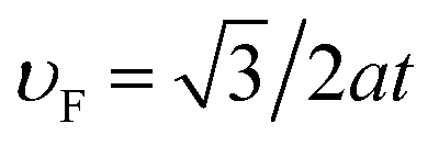
| HStable = (Mςz,sz + UEF)σz + υF(ςzkxσx − kyσy) | (4) |
 . In the above equation, ς, s and σ are the Pauli matrix acting in the space of valley, spin and sublattice space respectively. Uh-BN is the substrate potential of the heterostructure. Both valley and spin matrix are conserved here. The U parameter is induced due to presence of vertical electric field in the asymmetric heterostructure in our calculations. In case of symmetric trilayer heterostructure, it is a good approximation to consider Uh-BN as 0 to get best fit of TB parameters with the DFT based simulations. Thus, the presence of the Uh-BN term is neglected in the Hamiltonian eqn (1). A small nonzero value of the parameter Uh-BN = −28.7 meV is taken in case of asymmetric bilayer graphene/h-BN structure, which is uniform throughout the system and perpendicular to the heterolayer. TB parameters for symmetric structure, Uh-BN = 0 and other hopping parameters (t, t′, tso) = (0.85 eV, 1.09 eV, 28.7 meV) have been kept same in case of asymmetric bilayer structure. These parameters of TB model for both the structures are fitted with the DFT based band structures and DOS calculations.
For an explicit valley and spin values, the corresponding projected topological charges can be written as,
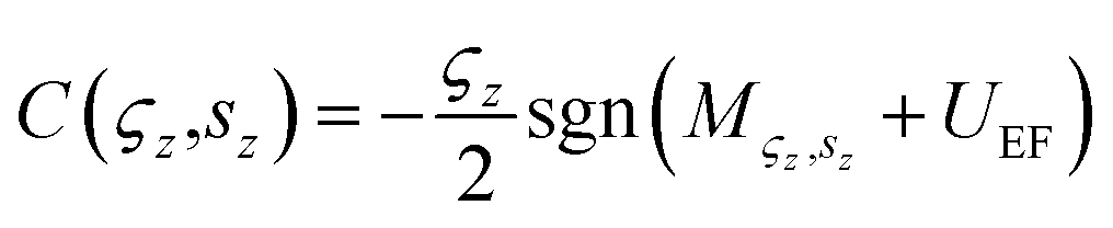 | (5) |
This equation is readily used to calculate total Chern numbers (C), spin Chern numbers (Cup/down), topological invariant (Z2) and valley Chern numbers (CK/K′) which are written as, 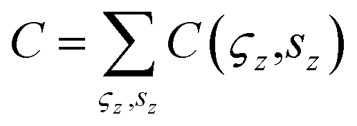 ,
, 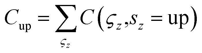 ,
,  , Z2 = (Cup + Cdown)/2 and
  . Based on the conservation principle of spin and valley numbers, both spin and valley quantum numbers are well fitted with the TB model in our calculation. Taking the above formulae, we have calculated the value of Z2 for asymmetric and symmetric structures. This approach is validated by performing with direct self-consistent first principles calculations under applied electric field. Moreover, the results obtained from TB model has been corroborated with the DFT results in case of density of states and band structure. An external electric field is applied along z-direction (Fig. 1(k)) of the simulation cell to compensate the staggered potential of the substrate.
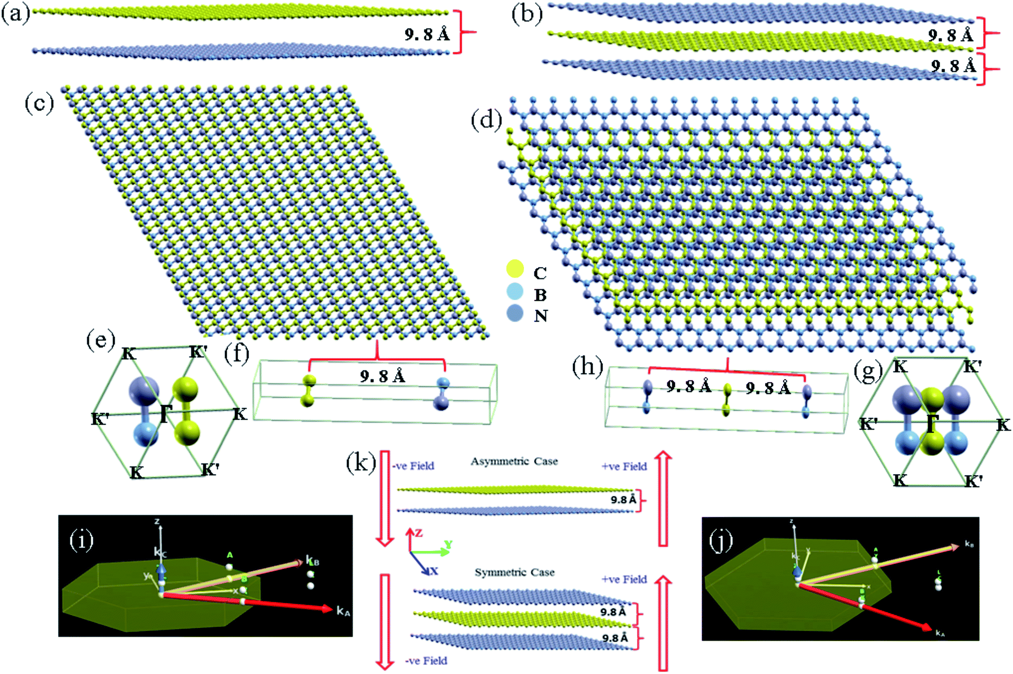 | ||
| Fig. 1 Crystal structure of asymmetric and symmetric heterostructures. (a) Side and (c) top view of the crystal structure of asymmetric heterostructures. (b) and (d) similar as (a) and (c) but for symmetric ones. (e), (f) and (i) are the hexagonal unit cell, supercell with interplanner spacing and first Brillouin zone for asymmetric case respectively. Same presentation in (g), (h) and (j) for symmetric case respectively. (k) Schematic representation of in-plane external electric field applied along perpendicular z-axis in both positive and negative direction. | ||
Results and discussions
A. Surface atomic configuration
The optimized structures of the heterobilayers are determined using geometry optimization with the Broyden–Fletcher–Goldfarb–Shanno (BFGS) algorithm.39 The calculation is followed by moving the constituting atoms to the positions where the total energy is minimum with stable structure. The structures of the heterolayers are shown in Fig. 1. The geometry and corresponding interlayer distances are determined by employing the atomic structure optimization.B. Electronic structure
The density of states (DOS) for both the cases has been calculated to find the number of states and band gap (shown in Fig. 2). The states are more flat near Fermi (Ef) region in case of asymmetry structure comparing to their symmetric counterpart indicating closing of bandgaps in symmetric cases. We have observed the signature of flatness in case of non-spin orbit coupling case. SoC has given closed gap with more dense states away from Ef. Twice the value of DOS intensity in case of symmetric structures retains its trilayer sandwich pattern.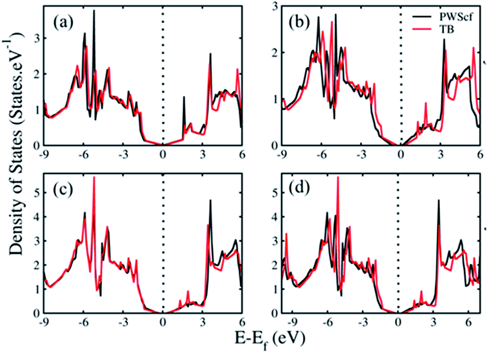 | ||
| Fig. 2 Density of states calculation for both asymmetric (a) NSoC and (b) SoC cases. Similarly, for symmetric structure (c) NSoC and (d) SoC cases. The black dotted line presents the Fermi energy level. | ||
The TB approximation solves the one electron Schrödinger equation with high accuracy allowing many body electron–electron interaction. Moreover, these models are computationally efficient because of the small number of basis orbitals and the rigid nature of the Hamiltonian. As a result, the simulation effort of the calculations increases linearly with the system size and the model can be applied to other 2D materials and their heterostructure. Motivated by the merits of TB model, we have incorporated TB model with our DFT simulation. The TB model based density of states has been plotted along with the DFT derived states to compare the fitting of the two plots. We have found that both the two plots fitted well with a deviation of less than 4.3%. The bandgap values are 63 meV and 35 meV for NSoC and SoC cases for asymmetric structure respectively. The symmetric structure possesses lower values of bandgap and the digits are 17.3 meV and 3.9 meV for NSoC and SoC cases respectively. Closing of gap is clearly evident from asymmetric bilayer to symmetric trilayer system due to presence of highly dense states in symmetric structure. Moreover, inclusion of spin–orbit coupling signifies the gap closing and orbital splitting nature which is given in projections of the DOS.
To realize the orbital contribution and presence, we have projected the DOS in k space to get projected crystal wave function values named as projected density of states (PDOS). Here, we have resolved the case for carbon atom to show the PDOS (shown in Fig. 3). This orbital wave function value got replicated in case of SoC due to twice the number of spinors. We have taken two distinct wave functions to present both spin and orbit. This PDOS pattern reflects the orbital splitting which can be corroborated with the respected band structure (Fig. 4).
 | ||
| Fig. 3 Projected density of states calculation for both asymmetric (a) NSoC and (b) SoC cases. Similarly, for symmetric structure (c) NSoC and (d) SoC cases. The red dotted line presents the Fermi energy level. | ||
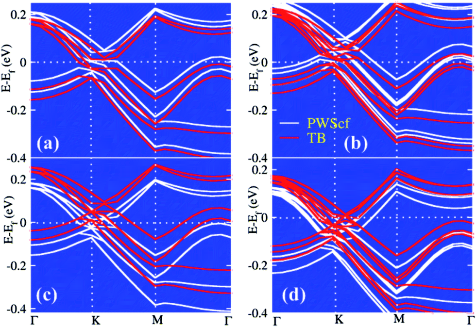 | ||
| Fig. 4 Electronic band structure of asymmetric (a) NSoC and (b) SoC case. Also, for symmetric heterostructures (c) NSoC and (d) SoC case with symmetric k-points named as Γ, K, M and Γ. The white dotted line parallel to x-axis shows the Fermi energy level. | ||
The PDOS pattern clearly indicates the reflection of all orbitals with Cs and Cp orbitals. There is no doubling in densities of projection in symmetric case unlike Fig. 2. This presents the equal contribution and projection of all orbitals that are present in the structures. In case of coupling, j–j coupling process is followed with (l + s) to (l − s) values for splitting. For s orbital, we have found two cases for s = 0.5. Similarly, for p orbital, we have found two cases p = 0.5 and p = 1.5. In case of p = 0.5, two states of projections are noted whereas for p = 1.5, 4 cases of projections are noted. This indicates the overall orbital contribution in case of coupling.
C. Topological phase transition
Topological insulators (TIs) with time-reversal symmetry have been becoming an interesting topic of research in condensed matter physics and material science during the last decade. Two dimensional (2D) TIs give rise to stable edge states which are retained by the time-reversal symmetry. This nature of 2D materials makes them suitable for spintronics and valleytronics applications.15,16 Moreover, these TIs exist intrinsically or can be induced by applying external field on the system. Motivated by the above inspiration, we have implemented the spin orbit (SO) coupling effect to realize the topological phase change and the variation in magnetic moment. In case of coupling between spin and atomic orbit, we have considered the j–j coupling method to replicate the presentation with double the number of spinor wave function.Finally, the moment per atomic site attends null value at the convergence iterative stage indication zero magnetic moment induction in the system. Band structure calculations (Fig. 4) show that the bands of h-BN substrate are away from the Fermi energy level, hence the h-BN substrate lacks hybridization with the relevant low-energy levels of the host sheet, but opens a trivial gap (62.32 meV) at the Dirac (K) point without SoC. Moreover, according to the calculation, with more layers of h-BN under those host materials, the band gap is changed in the range ∼40 meV, so it can be preferred to use a monolayer of h-BN as the substrate and the results could apply to the case of the several layers substrate. This gives birth towards the development of sandwich structure to form symmetric case. We have observed that in the absence of h-BN, the band structure profile will not change except for the gap closed in the freestanding pristine graphene sheet. This indicates the role of the substrate which exerts a staggered potential on the host sheet. To understand the origin of the staggered potential and its contraction, we have applied an external in-plane electric field along z-axial direction.
The topological invariant (Z2) is used to characterized the topological different phases for time-reversal invariant electronic systems and Z2 = 1 means topological nontrivial (TI or QSH phase) whereas Z2 = 0 indicates topological trivial (normal insulator) case. The invariant, Z2, is characterized by the band topology in presence of time-reversal symmetry. This Z2 classification gives an appropriate difference between two distinct time reversal topological and trivial phases. Moreover, the invariant (Z2) can be explicitly obtained from band parity calculation of the heterostructure system with inversion symmetry.40 Pristine h-BN is a normal wide bandgap insulator. Upon inclusion of SoC effect, the system exhibits a QSH phase provided when the electronic properties of the system is influenced by external factors i.e. electric field or strain. Here, we have calculated the phase transition and electronic properties of the system in presence of in-plane electric field. In this approach, we have obtained the Z2 invariant values using the methods explained in the tight-binding section. This approach, when solving in the frame work of tight-binding, is quite efficient for 2D material system in both cases of asymmetric and symmetric structure.41 In a simplified form, the value of Z2 is calculated following an integral over half the Brillouin zone (HBZ) which is given by
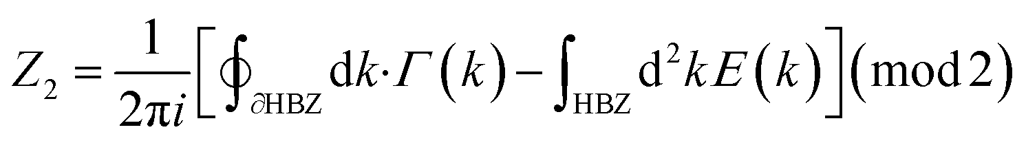 | (6) |
In the above equation, Γ(k) = ∑〈un(k)|∇nun(k)〉 is the Berry gauge potential and the Berry field strength is given as E(k) = |∇k × Γ(k)|z, where un(k) is the periodic part of the Bloch state with band index n and the summation process runs over all occupied states. Here, spin and valley are suitable quantum numbers to be considered, hence for specific spin and valley quantum number, the Berry curvature and connection of the valence bands with |uk〉 are calculated with the periodic parts of the Bloch wave functions, which has been discussed in eqn (5). Stoke's theorem shows that the result of the HBZ will vanish if both Γ and E have the same gauge. To overcome this condition, one needs to fix the gauge first with the help of additional constraints.42 After getting the fixed gauge, we can obtain the values of Z2 considering periodicity of k points and reciprocal lattice vector (G). The values of Z2 = 0 or Z2 = 1 represents the trivial (normal) or non-trivial (topological) phases, respectively at the moment when the gauge fixing is complete.43,44 In case of asymmetric NSoC, the band gap varies with the perpendicular external electric field (shown in Fig. 5) in a V like shape and centered at 0.2 V Å−1. For the SoC case, we have given a phase diagram, where topological phase transitions occur twice (at 0.1 and 0.3 V Å−1). The band gap varies with the electric field in a W like shape and centered at 0.2 V Å−1. Around the center of the W like shape, QSH insulating behavior can be predicted, whereas far from the center are based on band insulators. Similar conditions found in case of symmetric case with linearity in the band gap modulation. With application of electric field, the gap is varying from minimum to maximum presenting topological phase change (shown in Fig. 6). The parameters obtained from the TB model has been fitted with the DFT simulation results of band structure and DOS calculations. The existence of QSH and topological phases has been shown using first-order intrinsic SO coupling interaction in case of both asymmetric and symmetric heterostructure. This study proposes the suitability of the system for nanoelectronics based device application.
 | ||
| Fig. 5 Phase diagram in the plane of an external electric field and band gap for (a) asymmetric and (b) symmetric case. Dotted white lines are provided to guide the viewer's eye. | ||
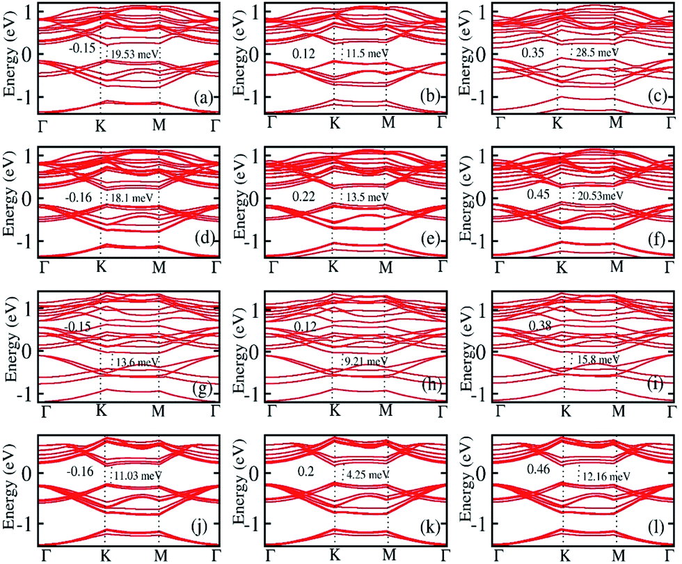 | ||
| Fig. 6 Variation of band gap with respect to applied in-plane perpendicular electric field with different value of field in positive and negative direction. Asymmetric (a) to (c) NSoC and (d) to (f) SoC cases. Similarly, symmetric (g) to (i) NSoC and (j) to (l) SoC case. | ||
The above found results point to the possibility of an electrical control of the on/off state of charge or spin conductance mechanism of the edge states, which would have positive implications for QSH based electronic devices.45–50 Here, we propose a field effect transistor (FET) based on vdW heterostructures of graphene monolayer and 2D wide-gap insulators (i.e. h-BN). The proposed device model is sketched in Fig. 7, where the top and bottom gates supply the in-plane vertical electric field to control the on/off function. 2D h-BN insulates its adjacent QSH layers electrically, hence parallel helical edge channels in the device model are protected from being gapped by interlayer hybridization.51 This property helps to increase the number of edge transport channels parametrically. This device will support dissipation less charge/spin transport in the ‘on’ state (Z2 = 1, nontrivial case) under ideal conditions with a quantized electrical conductance of  , where N is the number of QSH layers used in the device.52 Applying a moderate electric field in vertical direction will transform graphene into a normal insulator (Z2 = 0, trivial case) and turn the edge conduction to ‘off’ (i.e. Z2 = 0) state (shown in Fig. 5). The operational mechanism of this proposed vdW based FET device application is fundamentally different from traditionally designed metal oxide semiconductor FETs (MOSFET). The proposed QSH insulators and their van der Waals heterostructures may provide a potential platform for realizing ample scope in the field of low dissipation quantum electronics and spintronics.
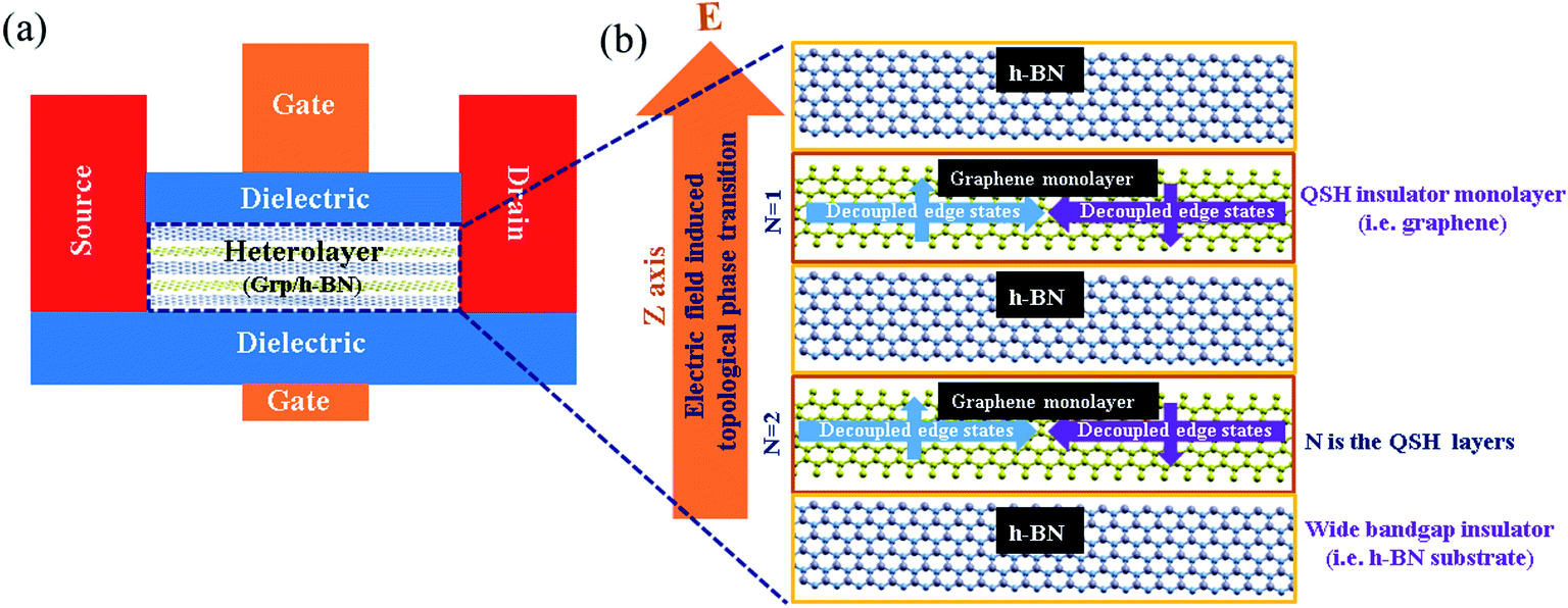 | ||
| Fig. 7 The proposed device model of vdW-FET. (a) Schematic of vdW-FET. (b) The central component of the model device is a vdW heterostructure of alternating layers of wide-gap insulator (i.e. hBN) and QSH graphene monolayer. Carriers (charge or spin) are injected from the source electrode and ejected into the drain electrode. Applied vertical electric field (i.e. along z-axis) will control the on/off switch through the top and bottom gates. | ||
Conclusions
In conclusion, we have studied the band topology of graphene/h-BN heterostructure with inclusion of spin–orbit coupling using DFT calculations and TB model based Hamiltonian. The edge states of the heterostructure exhibit an interesting band tuning and play an important role in transport property. Consequently, two different topological phases, including the QSH and weak topological insulating phases, are classified here. We find that both the valley Chern number and spin Chern number are quantized in these two topological phases. The transition from one topological phase to another is complemented by the band gap closing or opening. This provides an experimental platform to tune the topological states of graphene/h-BN heterostructure using external electric field. In the presence of a finite in-plane field, the weak TI phase as well as the QSH phase coexists with broken time-reversal symmetry on condition that the effect of SoC wins over time-reversal symmetry breaking. The sandwich structure retains the atomic configuration of the host materials by stabilizing the geometry and protects the intrinsic electronic properties from the undesired influence of the substrates. Controlled field mobility in the heterostructure makes it suitable for model FET application. We hope that these tunable topological strategies will be realized to develop novel adaptive structures and their application in spintronics and valleytronics.Acknowledgements
PD acknowledges a UGC research award from University Grants Commission vide grant no. F.30-1/2014/RA-2014-16-GE-WES-5629 (SA-II) dated 20.02.2015. S. K. B. acknowledges Department of Science & Technology (DST), Government of India for providing financial support in terms of INSPIRE Fellowship. S. K. B. also likes to thank Department of Computer Science, Tezpur University for providing cluster computing facility.References
- K. Geim and I. V. Grigorieva, Nature, 2013, 499, 419 CrossRef PubMed.
- H. Pan, et al., Phys. Rev. B: Condens. Matter Mater. Phys., 2015, 91, 045404 CrossRef.
- H. Pan, et al., Phys. Rev. Lett., 2014, 112, 106802 CrossRef PubMed.
- G. G. Guzmán-Verri and L. C. Lew Yan Voon, Phys. Rev. B: Condens. Matter Mater. Phys., 2007, 76, 075131 CrossRef.
- B. Roy, J. Hofmann, V. Stanev, J. D. Sau and V. Galitski, Phys. Rev. B: Condens. Matter Mater. Phys., 2015, 92, 245416 CrossRef.
- H. Zhao, et al., Phys. Chem. Chem. Phys., 2016, 18, 31862 RSC.
- Y. Ding and J. Ni, Appl. Phys. Lett., 2009, 95, 083115 CrossRef.
- Z. Ni, et al., Nano Lett., 2012, 12, 113 CrossRef CAS PubMed.
- G. Qin, et al., Nanoscale, 2017, 9, 7227 RSC; A. Ramasubramaniam, et al., Nano Lett., 2011, 11, 1070 CrossRef CAS PubMed.
- M. Ezawa, Phys. Rev. Lett., 2012, 109, 055502 CrossRef PubMed; J. E. Padilha, et al., J. Phys.: Condens. Matter, 2012, 24, 075301 CrossRef PubMed.
- J. Zhang, et al., Sci. Rep., 2015, 5, 10629 CrossRef PubMed.
- H. Pan, et al., Phys. Rev. B: Condens. Matter Mater. Phys., 2015, 92, 041404 CrossRef.
- M. Wang, et al., Phys. Rev. B: Condens. Matter Mater. Phys., 2016, 93, 155412 CrossRef.
- Z.-X. Guo, et al., Phys. Rev. B: Condens. Matter Mater. Phys., 2013, 87, 235435 CrossRef CAS; D. Kim, et al., Surf. Sci., 2013, 610, 27 CrossRef.
- D. Xiao, M.-C. Chang and Q. Niu, Rev. Mod. Phys., 2010, 82, 1959 CrossRef CAS.
- X. L. Qi and S. C. Zhang, Rev. Mod. Phys., 2011, 83, 1057 CrossRef CAS.
- S. K. Behera, P. Deb and A. Ghosh, Phys. Chem. Chem. Phys., 2016, 18, 23220 RSC; S. K. Behera, et al., ChemistrySelect, 2017, 2(13), 3657 CrossRef CAS.
- M. Z. Hasan and C. L. Kane, Rev. Mod. Phys., 2010, 82, 3045 CrossRef CAS.
- L. Tao, et al., Nat. Nanotechnol., 2015, 10, 227 CrossRef CAS PubMed.
- W. Wang, et al., Nat. Mater., 2013, 12, 792 CrossRef PubMed.
- P. Giannozzi, et al., J. Phys.: Condens. Matter, 2009, 21, 395502 CrossRef PubMed.
- G. Kresse and D. Joubert, Phys. Rev. B: Condens. Matter Mater. Phys., 1999, 59, 1758 CrossRef CAS.
- J. P. Perdew, K. Burke and M. Ernzerhof, Phys. Rev. Lett., 1996, 77, 3865 CrossRef CAS PubMed.
- A. Tkatchenko and M. Scheffler, Phys. Rev. Lett., 2009, 102, 073005 CrossRef PubMed.
- H. J. Monkhorst and J. Pack, Phys. Rev. B: Solid State, 1976, 13, 5188 CrossRef.
- D. N. Sheng, et al., Phys. Rev. Lett., 2006, 97, 036808 CrossRef CAS PubMed.
- W.-F. Tsai, et al., Nat. Commun., 2013, 109, 055502 Search PubMed.
- C. L. Kane and E. J. Mele, Phys. Rev. Lett., 2005, 95, 226801 CrossRef CAS PubMed.
- H. Min, et al., Phys. Rev. B: Condens. Matter Mater. Phys., 2006, 74, 165310 CrossRef.
- Y. G. Yao, et al., Phys. Rev. B: Condens. Matter Mater. Phys., 2007, 75, 041401(R) CrossRef.
- M. Gmitra, et al., Phys. Rev. B: Condens. Matter Mater. Phys., 2009, 80, 235431 CrossRef.
- A. H. Castro Neto and F. Guinea, Phys. Rev. Lett., 2009, 103, 026804 CrossRef CAS PubMed.
- C. Weeks, et al., Phys. Rev. X, 2011, 1, 021001 Search PubMed.
- Y. S. Dedkov, et al., Phys. Rev. Lett., 2008, 100, 107602 CrossRef PubMed.
- O. Rader, et al., Phys. Rev. Lett., 2009, 102, 057602 CrossRef CAS PubMed.
- A. Varykhalov, et al., Phys. Rev. Lett., 2008, 101, 157601 CrossRef CAS PubMed.
- V. Tran, et al., Phys. Rev. B: Condens. Matter Mater. Phys., 2014, 89, 235319 CrossRef.
- E. T. Sisakht, et al., Phys. Rev. B: Condens. Matter Mater. Phys., 2015, 91, 085409 CrossRef.
- J. D. Head and M. C. Zerner, Chem. Phys. Lett., 1985, 122, 264 CrossRef CAS.
- L. Fu and C. L. Kane, Phys. Rev. B: Condens. Matter Mater. Phys., 2007, 76, 045302 CrossRef.
- A. N. Rudenko and M. I. Katsnelson, Phys. Rev. B: Condens. Matter Mater. Phys., 2014, 89, 201408 CrossRef.
- A. A. Soluyanov and D. Vanderbilt, Phys. Rev. B: Condens. Matter Mater. Phys., 2011, 83, 035108 CrossRef.
- C. L. Kane and E. J. Mele, Phys. Rev. Lett., 2005, 95, 146802 CrossRef CAS PubMed.
- L. Fu and C. L. Kane, Phys. Rev. B: Condens. Matter Mater. Phys., 2006, 74, 195312 CrossRef.
- J. Wunderlich, et al., Science, 2010, 330, 1801 CrossRef CAS PubMed.
- D. Pesin and A. H. MacDonald, Nat. Mater., 2012, 11, 409 CrossRef CAS PubMed.
- F. Mahfouzi, N. Nagaosa and B. K. Nikolić, Phys. Rev. Lett., 2012, 109, 166602 CrossRef PubMed.
- C. Brüne, et al., Nat. Phys., 2012, 8, 485 CrossRef.
- C. H. Li, et al., Nat. Nanotechnol., 2014, 9, 218 CrossRef CAS PubMed.
- A. R. Mellnik, et al., Nature, 2014, 511, 449 CrossRef CAS PubMed.
- C. R. Dean, et al., Nat. Nanotechnol., 2010, 5, 722 CrossRef CAS PubMed.
- X. Qian, J. Liu, L. Fu and J. Li, Science, 2014, 346, 1344 CrossRef CAS PubMed.
Footnote |
| † Electronic supplementary information (ESI) available. See DOI: 10.1039/c7ra06069f |
| This journal is © The Royal Society of Chemistry 2017 |