DOI:
10.1039/C7RA05837C
(Paper)
RSC Adv., 2017,
7, 34810-34815
Crack-based strain sensor with diverse metal films by inserting an inter-layer†
Received
24th May 2017
, Accepted 5th July 2017
First published on 11th July 2017
Abstract
Various sensory systems to detect human motions have been developed for wearable healthcare and artificial electronic skins. Recently, an ultrasensitive mechanical crack-based strain sensor inspired by a spider's slit organ has been proposed. In spite of its high sensitivity, flexibility, and fascinating sensing ability to vibration, the materials that can be used to manufacture the sensor are limited to certain kinds because of the low adhesion between the substrate and a metal film. Therefore, the compatibility of materials with the substrate is a crucial issue in developing a practical sensor system. Here, we present a mechanical crack-based strain sensor with diverse metal (Au, Ag and Pt) films by introducing an inter-layer. Two inter-layers are used; a Cr layer is for generating cracks and MoO3 layer for enhancing the adhesion between the substrate and the metal layer. When cracks are generated on the Cr layer, they are propagated to the conductive metal layers (Au, Ag and Pt). Our crack-based strain sensor exhibited reproducibility and durability with high sensitivity to strain (GF = ∼1600 for Au and Ag layered crack sensors at 2% strain, GF = ∼850 for Pt layered sensor at 2% strain).
1. Introduction
A sensing mechanism for human motions on the skin has been extensively studied in diverse engineering research fields.1–6 Various sensory systems have been developed to have precision,1,7,8 lightness,3 flexibility,2,6,9 and attachability to adapt to human interfaces.10–12 Dealing with these issues, some studies have presented sensory systems that make use of graphene,13–15 carbon nanotubes,16–18 and metal nanowires combined with polymer substrates.19,20 These sensing systems successfully detect human motions such as facial expression, finger motion, vocal recognition, pulse, blood rate, and temperature change. Of these, a mechanical crack sensory system has recently been reported by using generated cracks on a polymeric substrate.1,7,8,21–23 The system showed high sensitivity defined by a linearly defined gauge factor (GF), with high durability and flexibility. The mechanical crack sensory system is composed of a Pt metal layer as a conductive layer, and a polyurethane acrylate (PUA) layer as the substrate which is used to induce cracks on the Pt metal layer. However, the PUA substrate is not compatible to be directly deposited with other metals including gold (Au) and silver (Ag) to generate defined cracks to sense motions, because of the low adhesion between the substrate and the metal film.24,25 This poses huge restrictions in the choice of materials. In the interaction of the metal layer and the polymeric layer for which adhesive force is an essential factor, compatibility is a very crucial issue in the field of sensory systems. In order to deal with this issue, inserting new inter layers could be a solution. Herein, we present an alternative mechanical crack sensory system with diverse materials (Au, Ag and Pt) by introducing a brittle metal Cr layer to generate cracks to the other ductile metal layer with an oxide layer to enhance adhesion of the metal layer to the PET film.26 Our sensor has exhibited high sensitivity to strain (the GF of Au and Ag metal layered crack sensors is about 1600 at a strain of 2% and that of a Pt metal layered crack sensor is about 850), reproducibility and durability.
2. Experimental section
2.1 Metal layered crack sensors fabrication
The size of metal layered crack sensors is 6.5 mm width and 40 mm height length. 5 nm of MoO3 and 10 nm of Cr are deposited on the 30 μm polyethylene terephthalate (PET) film by a thermal evaporator (Selcos Co., LTD.). On top of the Cr layer, 20 nm of Au or Ag is deposited by the thermal evaporator. Deposition rate of Au and Ag is 0.1 nm s−1. Besides, Pt is deposited on the Cr layer by a sputter (Q300TD, Tescan Korea). For each metal layered crack sensor, cracks are generated on the sensors from stretching by a material testing machine (3342 UTM, Instron Co.).
2.2 Measurement of resistance variation of metal layered crack sensors
Metal layered crack sensors are stretched by the material testing machine. The sensors are stretched with a strain from 0 to 2%. To measure the durability, the sensors were repeatedly stretched up to 5000 times. Resistance variance of metal layered crack sensors is measured by a Lab View-based PXI-4071 system (National Instruments Inc.).
3. Results and discussion
3.1 Composition of metal layered crack sensors
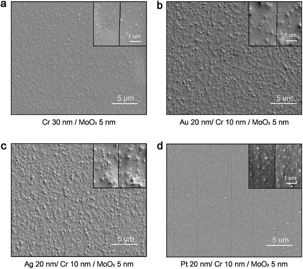
The schematic image in Fig. 1a shows the composition of the universal metal crack sensor. The crack sensor is composed of four layers, which are a conductive metal layer (Au, Ag, or Pt), an adhesion layer (Cr), a brittle oxide layer (MoO3), and lastly substrate (PET) on the bottom. Thermal evaporator deposits a conductive metal layer (Au, Ag, or Pt), MoO3 layer and Cr layer, of 20 nm, 5 nm and 10 nm, respectively, on a PET substrate film of 30 μm thickness. Fig. 1b is a photo image of the crack sensor devices including several kinds of metal layers on the top. For the conductive metal layer, Au, Ag, and Pt are used. These three metals have low electrical resistivity (Au: 22.14 nΩ m, Ag: 16.87 nΩ m, Pt: 105 nΩ m at 20 °C) and high ductility, so that these metal films typically do not make cracks on a PET substrate directly within strain of 2% (Fig. S1†).24,25 The key idea of the universal metal crack sensory system is to use a brittle oxide layer as an interlayer to make stable cracks on a ductile metal layer so that we can detect the resistance change of the universally cracked conductive metal layer with the applied strain (Fig. 1c). The resistance change of the sensory system is characterized by the crack state. The resistance is increased as the opened cracks reduce the conductivity of the conductive metal layer while strain is applied on the sensors. In contrast, the resistance is decreased as the cracks are closed while the strain is released.1 Fig. S1† shows the FESEM images of the conductive materials deposited on the PET substrates without any interlayers. Although these substrates have been stretched with strain of 2%, the images show that no crack has been generated on the metal layers. Eventually, a brittle material Cr was used to form cracks under the conductive materials. Cr is brittle enough to generate cracks beyond strain of 2% (Fig. S2†). The SEM image in Fig. 2a shows the FESEM image of Cr/MoO3 layers deposited on the PET substrate after stretched with strain of 2%. This image presents that the cracks are well generated with regular intervals. When two layers are tightly bonded together, cracks on one side can be propagated to the other layer.1 Since the Cr layer is well known as an adhesion layer of Au, Ag and Pt layers,24 the cracks initiated from the Cr layer are well propagated to the conductive material layer. Fig. 2b–d show the FESEM image of the Au, Ag and Pt layered crack sensor with an interlayer (Cr and MoO3). Interestingly, all of the conductive material layer crack sensors have the cracks with regular intervals similar with Fig. 2a. The average distance between the cracks of the Cr layer on PET substrate after stretching with strain of 2% is about 4.7 μm. Similarly, the average distance between the cracks of Au, Ag and Pt layered crack sensors are about 4.8 μm, 4.4 μm, and 5.0 μm, respectively. The cracks on the Cr layer and on the conductive material layer crack sensor display similarity in their distance from each other, because they propagate from the Cr layer onto the conductive layer.24,25 However, the existence of only Cr layer without MoO3 layer as inter-layers between the conductive layer and the substrate make the sensor less durable since the Cr metal layer is not well attached on the PET substrate. Fig. S3† is the graph of the durability test of a Pt layered crack sensor without MoO3 layer. Since the adhesion between the PET substrate and the metal films is poor, the gauge factor of the sensor decreases 850 to 370 within 650 cycles. To handle this problem, 5 nm of MoO3 layer as an adhesive layer is deposited between PET substrates and the Cr layer.26 And we have confirmed that the sensor with an only MoO3 layer without Cr layer does not generate cracks even with strain of 2%, which result indicates that the MoO3 layer only act as an adhesive layer (Fig. S4†).
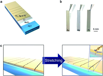 |
| | Fig. 1 Schematic images of a metal layered crack sensor. (a) The image of a metal layered crack sensor with Cr and MoO3 interlayers. (b) The real image of metal layered crack sensors. The sensors on the left side is an Au layered crack sensor. The sensors in the center are Ag layered crack sensors. The sensors on the right side are Pt layered crack sensors. (c) The illustration of the cracks on the sensor before stretching (left), and the cracks after stretching (right). The cracks on the conductive metal layer are induced by the cracks on the interlayer underneath the metal layer (the inserted image). | |
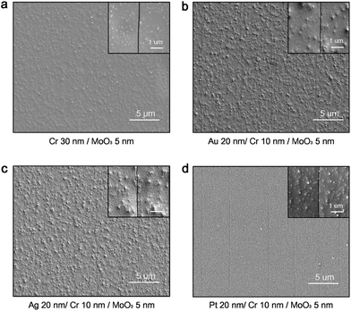 |
| | Fig. 2 SEM images of the metal layered crack sensors. (a) The SEM image of Cr (30 nm) and MoO3 (5 nm) on the PET substrate after strain of 2%. The inserted image is a magnified image of a crack on the Cr and MoO3 layered PET substrate. (b) The SEM image of an Au layered crack sensor after strain of 2%. The inserted image is a magnified image of a crack on the Au layered crack sensor. (c) The SEM image of an Ag layered crack sensor after strain of 2%. The inserted image is a magnified image of a crack on the Ag layered crack sensor. (d) The SEM image of a Pt layered crack sensor after strain of 2%. The inserted image is a magnified image of a crack on the Pt layered crack sensor. | |
3.2 Measurements of the performance of the metal layered crack sensors
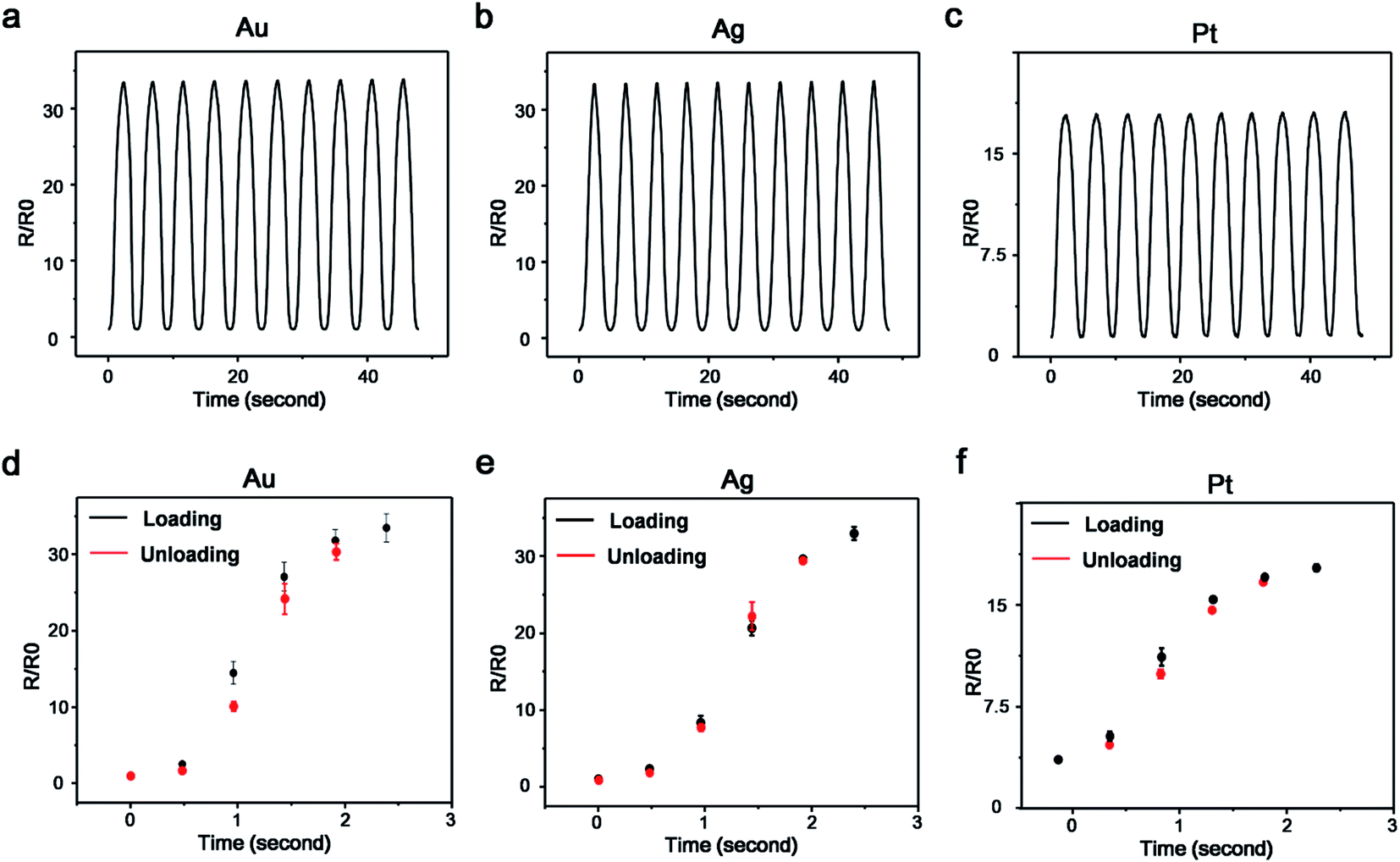
Fig. 3 shows the results of normalized resistance variation with strain for various metal layers. Fig. 3a is the graph of 10 cycles of the normalized resistance (R/R0) variance of the Au layer crack sensor that varies from 0% to 2% of strain. The linearly defined gauge factor (GF, ((R − R0)/R0)/ε) is over 1600. Fig. 3b is the graph of 10 cycles of the normalized resistance variance of the Ag layer crack sensor that varies from 0% to 2% of strain. The GF is over 1700. Fig. 3c is the graph of 10 cycles of the normalized resistance variance of the Pt layer crack sensor that varies from 0% to 2% of strain. The GF is over 900. We compare the conductive material layer crack sensors with the conductive material layer PET substrates without Cr and MoO3 layers. Fig. S5† is the graph of comparing the normalized resistance variances between the conductive material layer crack sensors and conductive material layer PET substrates without Cr and MoO3 layers with strain from 0% to 2%. Fig. S5a† is the graph of comparing the normalized resistance variances between an Au layer crack sensor (black line) and the Au layered PET substrate without Cr and MoO3 layers (red line). Since the Au layer on the PET substrate is ductile, it does not generate cracks on the Au layer with strain from 0% to 2% (Fig. S1a†). As a result, the Au layer on the PET substrate shows only slight normalized resistance change with strain from 0% to 2%. Fig. S5b† is the graph of comparing the normalized resistance variances between an Ag layer crack sensor (black line) and the Ag layered PET substrate without Cr and MoO3 layers (blue line). Fig. S5c† is the graph of comparing the normalized resistance variances between a Pt layer crack sensor (black line) and the Pt layered PET substrate without Cr and MoO3 layers (green line). Like the Au layered PET substrate, Ag and Pt layered PET substrates without Cr and MoO3 layers show only slight normalized resistance change with strain from 0% to 2%.
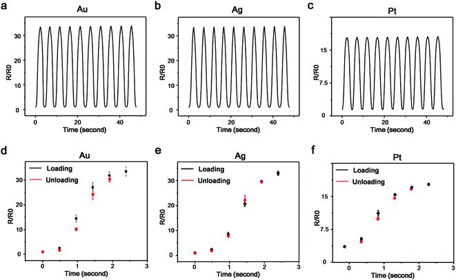 |
| | Fig. 3 The Performance graph of the metal layered crack sensors. (a) The graph of the Au layered crack sensors' normalized resistance variance versus strain of 2% in 10 cyclic tests. (b) The graph of the Ag layered crack sensors normalized resistance variance versus strain of 2% in 10 cyclic tests. (c) The graph of the Pt layered crack sensors normalized resistance variance versus strain of 2% in 10 cyclic tests. (d) The average and standard deviations of the 5 different Au layered crack sensors with hysteresis tests. Red dots show the unloading process and black dots show the loading process. (e) The average and standard deviations of the 5 different Ag layered crack sensors with hysteresis tests. Red dots show the unloading process and black dots show the loading process. (f) The average and standard deviations of the 5 different Pt layered crack sensors with hysteresis tests. Red dots show the unloading process and black dots show the loading process. | |
A previous study by Kang et al.1 has fabricated the mechanical crack sensory system with Pt layer, PUA layer and a PET substrate. In this case, the PUA layer acts as the Cr layer of the conductive material layer crack sensors. Fig. S6a and b† is the FESEM image of Au and Ag layer with the PUA layer and a PET substrate after stretching with strain of 2%. Both images show the Au and Ag layers with fine cracks on their surface that are generated by the PUA layers and transferred to them. However, even though the Au layer on the PUA layer has the cracks, it does not change the normalized resistance while it is stretched with strain of 2%.27 Fig. S7† is a comparative graph of the normalized resistance variance of the conductive material layer on the PUA layer and the conductive material layer crack sensors according to the strain of 2% in 10 cycles. Fig. S7a† is the graph of comparing the normalized resistance variance between the Au layer crack sensor (black line) and the Au layer on the PUA layer (red line) with strain from 0% to 2%. The Au layer on the PUA layer shows negligible normalized resistance change compared to the resistance change of the Au layer crack sensor. Fig. S7b† is the magnified graph of the normalized resistance change of the Au layer on the PUA layer with strain from 0% to 2%. Fig. S7c† is the graph of comparing the normalized resistance variance between the Ag layer crack sensor (black line) and the Ag layer on the PUA layer (blue line) with strain from 0% to 2%. Likewise, the normalized resistance change with strain from 0% to 2% of Ag layer on the PUA layer is negligible. Fig. S7d† is the magnified graph of the normalized resistance change of the Ag layer on the PUA layer with strain from 0% to 2%. The reproducibility and hysteresis of conductive materials crack sensor are shown in Fig. 3d–f. Fig. 3d is the normalized resistance versus strain from 0% to 2% averaged over 5 different Au layer crack sensors along with error bars. Black dots represent the loading the sensors from 0% to the final strain of 2%, and red dots are for the unloading the sensors from 2% to the final strain of 0%. Likewise, Fig. 3e and f are graphs of the normalized resistance versus strain from 0% to 2% averaged over 5 different Ag and Pt layer crack sensors along with error bars. Black dots and red dots show normalized resistance when loading the sensors from 0% to 2%, and from 2% to 0%, respectively. Through Fig. 3d–f, the loading/unloading hysteresis of conductive material layer crack sensors is little. The small error bars in these figures show that the conductive material layer crack sensors have a high reproducibility. The reversible test of the conductive material layer crack sensors with variation strain of 0.5%, 1% and 2% are shown in the graph of Fig. 4. Fig. 4a is the reversible test of the Au layer crack sensor, Fig. 4b the test of the Ag layer crack sensor, and Fig. 4c the test of Pt layer crack sensor. The blue line is the strain from 0% to 2%, the red line is the strain from 0% to 2%, and the black line is the strain from 0% to 2%. The conductive material layer crack sensors show similar normalized resistance variance with strain from 0% to 0.5%, 1% and 2%. Another important performance is durability. We have performed 5000 cyclic tests to conductive material layer crack sensors. Fig. 4d–f are the durability tests of Au, Ag, and Pt layer crack sensors, respectively.
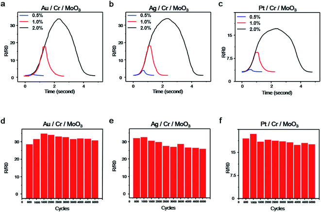 |
| | Fig. 4 The graph for reversible and marathon tests with the metal layered crack sensors. The reversible tests are performed with various strains of 0.5% (blue line), 1.0% (red line) and 2.0% (black line). (a) The reversible test of Au layered crack sensor. (b) The reversible test of Ag layered crack sensor. (c) The reversible test of Pt layered crack sensor. A marathon test of the conductive material layered sensors by repeating loading/unloading process about 5000 cycles at strain from 0% to 2%. (d) A final normalized resistance of a marathon test at a certain period with an Au layered crack sensor, (e) an Ag layered crack sensor and (f) a Pt layered crack sensor. | |
3.3 Detecting the hands motion by using metal layered crack sensors
The conductive material layer crack sensors detect human motions. We apply the Au layer crack sensors on the human fingers. Since the sensor is made on the PET substrate, it has flexibility to mount on a human hand by sticking the ends of the sensor onto the knuckles of each finger (Fig. 5). One of the experimenters put the two metal layered crack sensors on the knuckles of the index and ring fingers with the hand spread out as shown in Fig. 5a. Therefore, there is no resistance change of the crack sensors when the finger is spread. On the other hand, when the finger attached to the crack sensor is bent, the metal cracks on the sensor surface are opened and the resistance increases. In Fig. 5, we performed a rock-paper-scissors motion to verify that the crack sensors correctly indicate finger movements. Fig. 5b represents the clenching state of the hand, in which case the fingers are bent and the resistance of the crack sensor increases. In Fig. 5b, the hand is making a scissors motion for which the index finger is spread, while the ring finger is bent. Hence, there is resistance change in the Au layer crack sensor on the ring finger, while the crack sensor on the index finger shows no resistance change. In Fig. 5c, the hand is unfolded and there is no resistance change in the two Au layer crack sensors. The normalized resistance variances of the Au layer crack sensors with motion in the hand are shown in Fig. 5d, 4e and f. The red lines are the normalized resistance variance of the index finger, and the blue lines are the normalized resistance variance of the ring finger. As shown in these figures, the normalized resistance increases when the finger is bent and the resistance decreases when the finger is spread.
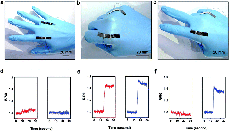 |
| | Fig. 5 Detecting the hands motion by Au metal layered crack sensors on the knuckles of the index and ring fingers (a) with the hand spread out, (b) with the hand clenched, (c) with the index finger spread out while the ring finger is clenched. (d) The graphs represent the Au metal layered crack sensors' normalized resistance variations due to the hand movement. The images on the left and right are the sensors on the index finger, and the ring finger, respectively, while (d) the hand spread out, (e) the hand clenched, and (f) the index finger spread out while the ring finger is clenched. | |
4. Conclusion
In conclusion, we report the Au, Ag and Pt layered crack sensor with inter-layers of Cr and MoO3. Brittle metal Cr layer was used for generating cracks to other ductile metal layer while the MoO3 layer was for enhancing adhesion between the PET film and the metal layers. Our sensor has exhibited high sensitivity to the applied strain (GF of Au and Ag metal layered crack sensors is about 1600 at the strain of 2% and that of a Pt metal layered crack sensor is about 850). The reversibility, reproducibility, and durability of these metal layered crack sensors showed adaptability in human motion detection such as hand motion sensing. Our proposed method to construct crack sensor with the inter-layers can be one of the breakthroughs to overcome the compatibility issue for the crack sensor with low-adhesion substrate.
Conflicts of interest
There are no conflicts of interest to declare.
Acknowledgements
M. Choi acknowledges financial support by the Global Frontier R&D Program of the Center for Multiscale Energy Systems (No. 2012M3A6A7054855) funded from the National Research Foundation (NRF) of Korea. D. Kang and S. M. Kim acknowledge financial support by Basic Science Research Program through the National Research Foundation of Korea (NRF) funded by the Ministry of Science, ICT & Future Planning (2016R1C1B1009689 and 2016R1C1B1014564). D. Kang acknowledges financial support by the new faculty research fund of Ajou University and the Ajou University research fund.
References
- D. Kang, P. V. Pikhitsa, Y. W. Choi, C. Lee, S. S. Shin, L. Piao, B. Park, K. Y. Suh, T. I. Kim and M. Choi, Nature, 2014, 516, 222 CrossRef CAS PubMed.
- S. Lee, A. Reuveny, J. Reeder, S. Lee, H. Jin, Q. Liu, T. Yokota, T. Sekitani, T. Isoyama, Y. Abe, Z. Suo and T. Someya, Nat. Nanotechnol., 2016, 11, 472 CrossRef CAS PubMed.
- D.-H. Kim, N. Lu, R. Ma, Y.-S. Kim, R.-H. Kim, S. Wang, J. Wu, S. M. Won, H. Tao and A. Islam, Science, 2011, 333, 838 CrossRef CAS PubMed.
- C. Pang, G. Y. Lee, T. I. Kim, S. M. Kim, H. N. Kim, S. H. Ahn and K. Y. Suh, Nat. Mater., 2012, 11, 795 CrossRef CAS PubMed.
- D. J. Lipomi, M. Vosgueritchian, B. C. Tee, S. L. Hellstrom, J. A. Lee, C. H. Fox and Z. Bao, Nat. Nanotechnol., 2011, 6, 788 CrossRef CAS PubMed.
- G. Schwartz, B. C. Tee, J. Mei, A. L. Appleton, D. H. Kim, H. Wang and Z. Bao, Nat. Commun., 2013, 4, 1859 CrossRef PubMed.
- T. Lee, Y. W Choi, G. Lee, P. V. Pikhitsa, D. Kang, S. M. Kim and M. Choi, J. Mater. Chem. C, 2016, 4(42), 9947 RSC.
- Y. W. Choi, D. Kang, P. V. Pikhitsa, T. Lee, S. M. Kim, G. Lee, D. Tahk and M. Choi, Sci. Rep., 2017, 7, 40116 CrossRef CAS PubMed.
- J. Lee, S. Kim, J. Lee, D. Yang, B. C. Park, S. Ryu and I. Park, Nanoscale, 2014, 6(20), 11932 RSC.
- S. Yang, Y. C. Chen, L. Nicolini, P. Pasupathy, J. Sacks, B. Su, R. Yang, D. Sanchez, Y. F. Chang, P. Wang, D. Schnyer, D. Neikirk and N. Lu, Adv. Mater., 2015, 27, 6423 CrossRef CAS PubMed.
- B. U. Hwang, J. H. Lee, T. Q. Trung, E. Roh, D. I. Kim, S. W. Kim and N. E. Lee, ACS Nano, 2015, 9, 8801 CrossRef CAS PubMed.
- E. Roh, B.-U. Hwang, D. Kim, B.-Y. Kim and N.-E. Lee, ACS Nano, 2015, 9, 6252 CrossRef CAS PubMed.
- S.-H. Bae, Y. Lee, B. K. Sharma, H.-J. Lee, J.-H. Kim and J.-H. Ahn, Carbon, 2013, 51, 236 CrossRef CAS.
- X. Li, R. Zhang, W. Yu, K. Wang, J. Wei, D. Wu, A. Cao, Z. Li, Y. Cheng, Q. Zheng, R. S. Ruoff and H. Zhu, Sci. Rep., 2012, 2, 870 Search PubMed.
- J. Shi, X. Li, H. Cheng, Z. Liu, L. Zhao, T. Yang, Z. Dai, Z. Cheng, E. Cheng, L. Yang, Z. Zhang, A. Cao, H. Zhu and Y. Fang, Adv. Funct. Mater., 2016, 26(13), 2078 CrossRef CAS.
- X. Zhang, S. Hu, M. Wang, J. Yu, Q. Khan, J. Shang and L. Ba, Nanotechnology, 2015, 26(11), 115501 CrossRef PubMed.
- Z. Liu, D. Qi, P. Guo, Y. Liu, B. Zhu, H. Yang, Y. Liu, B. Li, C. Zhang, J. Yu, B. Liedberg and X. Chen, Adv. Mater., 2015, 27, 6230 CrossRef CAS.
- J. Zhang, J. Liu, R. Zhuang, E. Mader, G. Heinrich and S. Gao, Adv. Mater., 2011, 23(30), 3392 CrossRef CAS.
- K. K. Kim, S. Hong, H. M. Cho, J. Lee, Y. D. Suh, J. Ham and S. H. Ko, Nano Lett., 2015, 15(8), 5240 CrossRef CAS.
- S. Gong, W. Schwalb, Y. Wang, Y. Chen, Y. Tang, J. Si, B. Shirinzadeh and W. Cheng, Nat. Commun., 2014, 5, 3132 Search PubMed.
- H. Song, J. Zhang, D. Chen, K. Wang, S. Niu, Z. Han and L. Ren, Nanoscale, 2017, 9(3), 1166 RSC.
- T. Yang, X. Li, X. Jiang, S. Lin, J. Lao, J. Shi, Z. Zhen, Z. Li and H. Zhu, Mater. Horiz., 2016, 3(3), 248 RSC.
- B. Park, J. Kim, D. Kang, C. Jeong, K. S. Kim, J. U. Kim, P. J. Yoo and T. I. Kim, Adv. Mater., 2016, 28(37), 8130 CrossRef CAS PubMed.
- B. Putz, R. L. Schoeppner, O. Glushko, D. F. Bahr and M. J. Cordill, Scr. Mater., 2015, 102, 23 CrossRef CAS PubMed.
- Y. Xiang, T. Li, Z. Suo and J. J. Vlassak, Appl. Phys. Lett., 2005, 87(16), 161910 CrossRef.
- T. Itoh, I. Matsubara, W. Shin and N. Izu, Thin Solid Films, 2006, 515, 27049 CrossRef.
- S. P. Lacour, S. Wagner, Z. Huang and Z. Suo, Appl. Phys. Lett., 2003, 82(15), 2404 CrossRef CAS.
Footnotes |
| † Electronic supplementary information (ESI) available. See DOI: 10.1039/c7ra05837c |
| ‡ These authors contributed equally to this work. |
|
| This journal is © The Royal Society of Chemistry 2017 |
Click here to see how this site uses Cookies. View our privacy policy here. 
 Open Access Article
 This Open Access Article is licensed under a Creative Commons Attribution-Non Commercial 3.0 Unported Licence
 *d and
Mansoo Choi*ab
*d and
Mansoo Choi*ab