
 Open Access Article
 This Open Access Article is licensed under a
 Creative Commons Attribution 3.0 Unported Licence
Facile chemical synthesis and enhanced thermoelectric properties of Ag doped SnSe nanocrystals†
Chia-Hua Chien‡
 abc,
Chung-Chieh Chang‡de,
Cheng-Lung Chen*c,
Chuan-Ming Tsengf,
Yu-Ruei Wuc,
Maw-Kuen Wuc,
Chih-Hao Leea and
Yang-Yuan Chen*c
abc,
Chung-Chieh Chang‡de,
Cheng-Lung Chen*c,
Chuan-Ming Tsengf,
Yu-Ruei Wuc,
Maw-Kuen Wuc,
Chih-Hao Leea and
Yang-Yuan Chen*c
aDepartment of Engineering and System Science, National Tsing Hua University, Hsinchu 30013, Taiwan
bNano Science and Technology Program, Taiwan International Graduate Program, Academia Sinica, National Tsing Hua University, Taiwan
cInstitute of Physics, Academia Sinica, Taipei 11529, Taiwan. E-mail: aabbss@gate.sinica.edu.tw; cheny2@phys.sinica.edu.tw
dSchool of Dental Technology, College of Oral Medicine, Taipei Medical University, Taipei 11031, Taiwan
eResearch Center of Digital Oral Science and Technology, College of Oral Medicine, Taipei Medical University, Taipei 11031, Taiwan
fDepartment of Materials Engineering, Ming Chi University of Technology, New Taipei City 24301, Taiwan
First published on 7th July 2017
Abstract
A two-step, surfactant-free solution growth process was utilized to synthesize p-type Ag doped SnSe nanocrystals in gram quantities. The formation mechanism of SnSe nanocrystals was studied by high resolution transmission electron microscopy, and it was shown that the main surface and edge facets are {100} and {011} respectively. A clear phase transition near 800 K was discovered in the temperature dependence of thermal conductivity. The thermoelectric properties of SnSe pellets prepared by spark plasma sintering exhibit a significant increase of zTmax (0.8 at 850 K) in the 3% Ag doped SnSe. The zTmax value is about 40% higher than that of the pristine SnSe. The consequence is mainly attributed to the enhancement of carrier concentration and power factor by Ag doping. Our results demonstrate that this facile chemical method is amenable to fabricate high quality SnSe nanocrystals and might also be applied to other anisotropic crystalline materials.
1. Introduction
Thermoelectric (TE) materials are an important topic in the research community due to their promising applications in waste heat recycling and device cooling.1 The energy conversion efficiency is governed by the figure of merit (zT) of materials defined as zT = (σS2/κ)T, where σ, S, κ, and T are electrical conductivity, Seebeck coefficient, thermal conductivity, and absolute temperature, respectively.2 Except for a superior Seebeck coefficient, a good TE material also requires excellent electrical transport properties and low thermal conductivity. In recent decades, a lot of strategies have been developed and applied to the existing state-of-the-art materials,3–5 and newly discovered materials6,7 for further improving their zT.A recent discrepancy on the intrinsic thermal conductivity of single crystalline SnSe between P. C. Wei et al.8 and L. D. Zhao et al.6 has attracted intense attention on this ultralow thermal conductivity compound. If the thermal conductivity is intrinsically 0.8 W m−1 K−1 verified by P. C. Wei et al., then the zT = 2.6 reported by L. D. Zhao et al. should be modified down to ∼1. So far more and more reports have begun to discuss the possible origins of these contradicting points.9–11
The stoichiometric SnSe is a semiconducting material with very low defect concentration and high resistivity. Appropriate element doping to SnSe can enhance its power factor and reduce its thermal conductivity with alloying effect. To date, doping effects on SnSe have been intensively investigated, and several dopants such as Ag,12 Na13–15 K,16 Ge,17–19 Cl,20 Te,21 Pb22 and S23 have been done. Na doping really improves the power factor of single crystalline SnSe, and reaches a higher zT for a broad temperatures.
Usually, most SnSe based samples with high zT are single crystalline, which usually needs more time and energy consumption in fabrication process. Here we report a much facile, bottom-up and surfactant-free chemical synthesis to prepare mass production of SnSe nanocrystals followed by spark plasma sintering process (SPS) to fabricate composited bulk of pristine and Ag doped SnSe. The growth mechanism and TE properties of these materials will be discussed. After extensively screen previous literatures of element doped SnSe samples that were chemically synthesized,24,25 We decide to grow SnSe nanocrystals with and without Ag dopants, which should have superior TE properties as that of single crystal of L. D. Zhao et al.6 In the work we did further improve the electrical conductivity and power factor of SnSe and achieve a 40% enhancement of zT (0.8 at 850 K) with 3% Ag doping as compared with the pristine SnSe. The results demonstrate that chemical method together with SPS technique can offer a rapid and large-scale synthesis route to fabricate high quality SnSe nanocrystals and their bulk composites.
2. Experimental
(AgxSn1−x)Se nanocrystals (x = 0, 0.01, 0.03 and 0.05) were synthesized by a facile surfactant-free synthesis method (Fig. 1), using NaOH (Sigma-Aldrich, ≥98%), ethylene glycol (EG, J. T. Baker, ≥99%), SeO2 (Alfa Aesar, 99.4%), SnCl2 (Alfa Aesar, 99%), hydrazine (Alfa Aesar, ≥98%), AgNO3 (Merck, ≥99.8%) as the chemical reagents. Firstly, 40 mmol SeO2 was added into a solution containing 90 mmol NaOH and 240 ml ethylene glycol (EG) at 373 K. Then, the Se source was obtained by slowly adding 7.2 ml hydrazine into above solution and kept at same temperature for 1 h. The valance of Se ion was reduced from 4+ into 0 in this step (SeO2 + N2H4 → Se + 2H2O + N2).24 Secondly, 90 mmol NaOH and 80 mmol SnCl2 were added into 60 ml EG at 413 K. In the meantime, the Ag source was prepared by reducing the AgNO3 with EG. The Sn and Ag source was mixed with the Se source, and stirred at 413 K for 15 h. The Sn2+ not only acted as Sn source but also the reducing agent (Sn2+ + Se → Sn4+ + Se2−; Sn2+ + Se2− → SnSe). The obtained black precipitates were immediately washed by deionized water/ethanol solutions, and collected by the centrifugation. The final products were dried under vacuum at 353 K for 24 h. The percent yield of the reaction is estimated to be approximately 87%. The chemical structure of nanocrystals was characterized by X-ray diffraction, using a diffractometer (XRD, PANalytical X'Pert Pro) equipped with Cu Kα radiation (λ = 0.154 nm). The microstructures, electron energy-loss spectroscopy (EELS) and selected area electron diffraction (SAED) patterns of nanocrystals were investigated by high resolution transmission electron microscopy (HRTEM, JEOL 2100F) with accelerating voltage of 200 kV. The powders were further pressed into bulks using spark plasma sintering (SPS-515S, SPS Syntex Inc.) at 500 K, 50 MPa under vacuum for 5 min to become a dense pellet of 12.7 mm in diameter and 12 mm in height. The size is large enough to be cut into small ingots for thermal and electrical transport measurements in the same direction. The relative density of all samples is higher than 90% of the theoretical value (6.18 g cm−3) (see ESI Table S1†). The Seebeck coefficient and electrical conductivity were carried out by a commercial system (ZEM-3, ULVAC-RIKO). The thermal conductivity was calculated from the relationship: κ = λρCp, where ρ, Cp, and λ are mass density, specific heat, and thermal diffusivity respectively. Mass density was measured by the Archimedes method. Specific heat and thermogravimetry were measured by a differential scanning calorimeter (DSC-STA-449, NETZSCH), and the thermal diffusivity was measured by a laser flash apparatus (LFA-457, NETZSCH). The Hall measurements were performed in a magnetic field up to ±2 T using a Physical Property Measurement System (PPMS, Quantum Design). The carrier concentration for the samples is calculated by nH = 1/|e|RH, where RH is the Hall coefficient. The carrier mobility is subsequently calculated from the relationship between electrical conductivity and carrier concentration, μH = σ/nH|e|. All presented data were measured along the same direction. The uncertainty of each electrical resistivity, Seebeck coefficient, and thermal conductivity measurements was estimated to be approximately 5%, which leads to a total experimental uncertainty of zT of approximately 20%.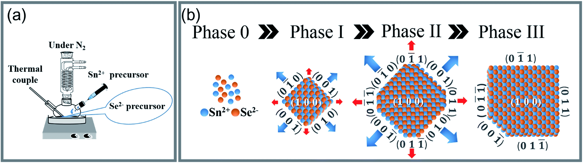 | ||
| Fig. 1 (a) The schematic configuration of a two-step chemical synthesis method. (b) The four phases of nanocrystal formation from Sn and Se atoms to the SnSe single crystal nanoplate. | ||
3. Results and discussion
3.1 Growth mechanism of SnSe nanocrystals and the structure characterizations
A synthesis yield > 10 g of (AgxSn1−x)Se (0 ≤ x ≤ 0.05) nanocrystals were synthesized with SnCl2, SeO2 and AgNO3 are Sn, Se and Ag sources respectively (Fig. 1). In the synthesis process, the morphology of nanocrystals is highly dependent on the surface energy (ε). The surface energy of an atomic plane can be expressed as:26
 | (1) |
![[1 with combining macron]](https://www.rsc.org/images/entities/char_0031_0304.gif) 0) (01) (001) and (011) were determined from the lattice fringes (Fig. 2b) and SAED (Fig. 2c), respectively. The inter-planar spacing of {011} is ∼0.3 nm and the angle between (01) and (011), (00) and (01) are 86° and 137°, respectively. The results fit well with the Pnma phase of SnSe. After 15 h, the reaction is almost completed and the growth of nanocrystals are terminated. Fig. 2d and f show that the final exposed edge facets of nanocrystals are {011} planes, and intersection angles between them are 86° and 94°. Furthermore, the compositions and the distributions of elements of SnSe and (Ag0.03Sn0.97)Se were analyzed using a scanning transmission electron microscope (STEM) (Fig. 3), confirming the homogeneous distribution of elements in specimen. We also performed the electron energy-loss spectroscopy (EELS) to substantiate the chemical form of SnSe. The results are presented in Fig. S1.† It can be seen that the peaks at 487 and 495 eV in the electron energy-loss spectrum correspond to the 3d5/2 and 3d3/2 peaks of Sn, respectively. The result demonstrates the presence of (+2) valence state of Sn in the nanocrystal. Moreover, the peak at 56 eV corresponds to the superposition of the 3d5/2 and 3d3/2 peaks for Se. These binding energy of 3d electronic states clearly verify the stoichiometry of SnSe. Furthermore, the scanning electron micrographs of fractured surfaces of a series of samples were investigated. The grains show platelet-like structures with a tendency to align and stack together, this results in a remarkably anisotropy in thermal and electrical transport properties. The average grain size of these samples is approximately 0.5–2 μm. The scanning electron microscopy images are presented in ESI Fig. S2.† The structure of (AgxSn1−x)Se nanocrystals were also examined using X-ray diffraction. All diffraction peaks are indexed to the low-temperature SnSe phase (PDF #00-014-0159) with an orthorhombic structure (Fig. 4a), and no impurity phases are observed within the detection limit. Additionally, the temperature dependence of structural evolution of pristine SnSe nanocrystals was investigated in situ (Fig. 4b). An obvious shift of characteristic peaks was observed as temperature increased, and this phenomenon was related to the process of phase transition from Pnma to Cmcm.6 Meanwhile, the dynamic structural behaviour of SnSe nanocrystals was also examined at thermal cycling by monitoring the XRD characteristic peaks of Pnma phase. In Fig. 4c, the evolution of these peaks are reversible in thermal cycle, confirming the second order phase transition.27 The lattice parameters determined from XRD are also plotted as a function of temperature (Fig. 4d). The lattice parameter a and b increase gradually with measured temperature, whereas the lattice parameter c reveals an opposite trend, revealing that the lattices shrink in c axis but extend in the ab plane.8,28 Finally, the cell volume linearly increases with the temperature, indicating a regular thermal expansion of the nanocrystals.
0) (01) (001) and (011) were determined from the lattice fringes (Fig. 2b) and SAED (Fig. 2c), respectively. The inter-planar spacing of {011} is ∼0.3 nm and the angle between (01) and (011), (00) and (01) are 86° and 137°, respectively. The results fit well with the Pnma phase of SnSe. After 15 h, the reaction is almost completed and the growth of nanocrystals are terminated. Fig. 2d and f show that the final exposed edge facets of nanocrystals are {011} planes, and intersection angles between them are 86° and 94°. Furthermore, the compositions and the distributions of elements of SnSe and (Ag0.03Sn0.97)Se were analyzed using a scanning transmission electron microscope (STEM) (Fig. 3), confirming the homogeneous distribution of elements in specimen. We also performed the electron energy-loss spectroscopy (EELS) to substantiate the chemical form of SnSe. The results are presented in Fig. S1.† It can be seen that the peaks at 487 and 495 eV in the electron energy-loss spectrum correspond to the 3d5/2 and 3d3/2 peaks of Sn, respectively. The result demonstrates the presence of (+2) valence state of Sn in the nanocrystal. Moreover, the peak at 56 eV corresponds to the superposition of the 3d5/2 and 3d3/2 peaks for Se. These binding energy of 3d electronic states clearly verify the stoichiometry of SnSe. Furthermore, the scanning electron micrographs of fractured surfaces of a series of samples were investigated. The grains show platelet-like structures with a tendency to align and stack together, this results in a remarkably anisotropy in thermal and electrical transport properties. The average grain size of these samples is approximately 0.5–2 μm. The scanning electron microscopy images are presented in ESI Fig. S2.† The structure of (AgxSn1−x)Se nanocrystals were also examined using X-ray diffraction. All diffraction peaks are indexed to the low-temperature SnSe phase (PDF #00-014-0159) with an orthorhombic structure (Fig. 4a), and no impurity phases are observed within the detection limit. Additionally, the temperature dependence of structural evolution of pristine SnSe nanocrystals was investigated in situ (Fig. 4b). An obvious shift of characteristic peaks was observed as temperature increased, and this phenomenon was related to the process of phase transition from Pnma to Cmcm.6 Meanwhile, the dynamic structural behaviour of SnSe nanocrystals was also examined at thermal cycling by monitoring the XRD characteristic peaks of Pnma phase. In Fig. 4c, the evolution of these peaks are reversible in thermal cycle, confirming the second order phase transition.27 The lattice parameters determined from XRD are also plotted as a function of temperature (Fig. 4d). The lattice parameter a and b increase gradually with measured temperature, whereas the lattice parameter c reveals an opposite trend, revealing that the lattices shrink in c axis but extend in the ab plane.8,28 Finally, the cell volume linearly increases with the temperature, indicating a regular thermal expansion of the nanocrystals.
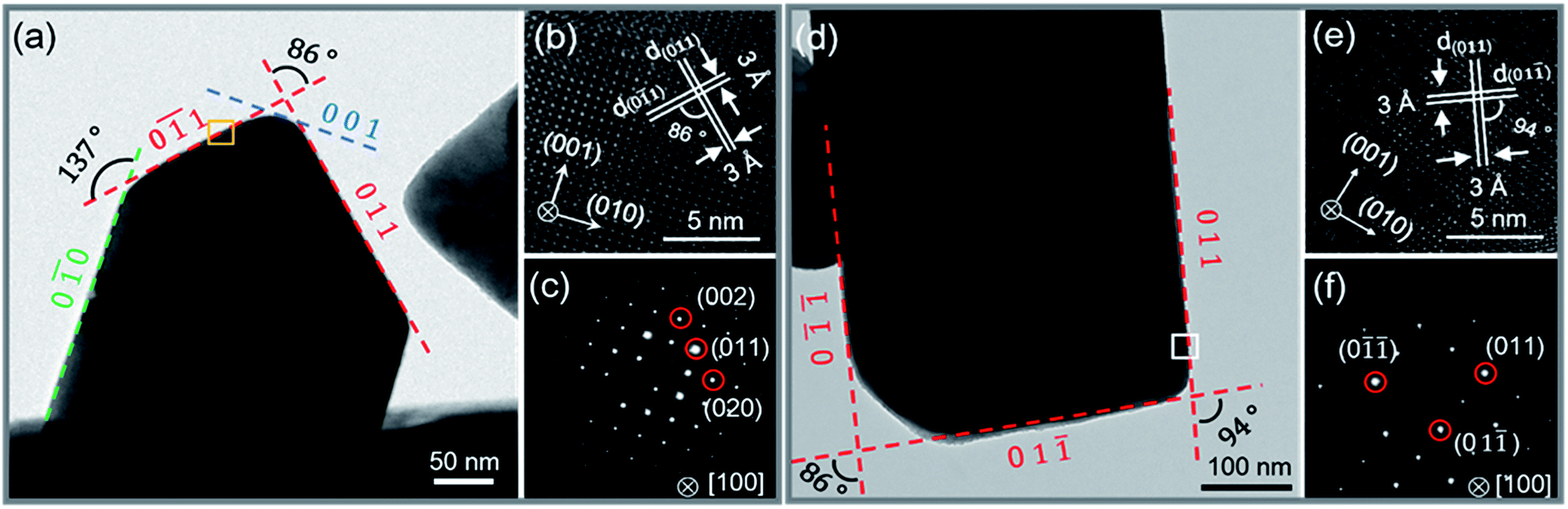 | ||
| Fig. 2 The TEM images of intermediate (a) and final (d) states of SnSe nanocrystals. (b) and (e) are the high-resolution TEM image taken from the orange and white areas in (a) and (d) respectively. The lattice spacing of 3 Å correspond to (011) plane. (c) and (f) are the SAED patterns of (b) and (e), reveal that SnSe nanocrystals taken along [100] projection. The SAED patterns are well indexed to the orthorhombic Pnma structure. | ||
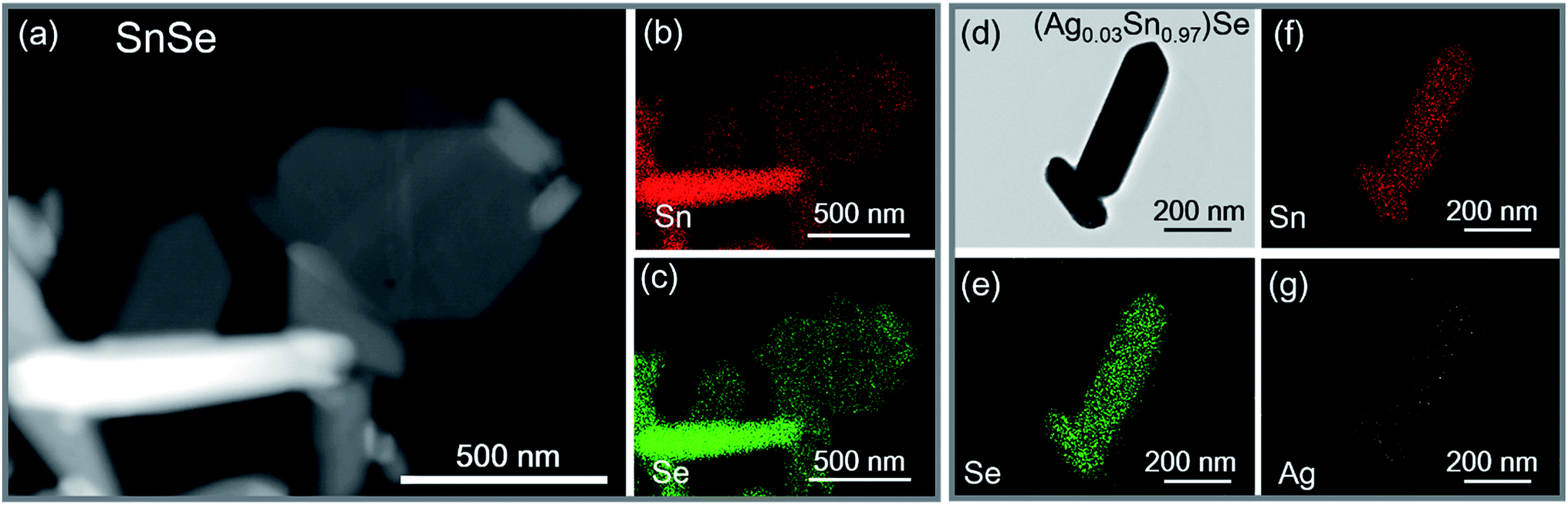 | ||
| Fig. 3 (a) HAADF-STEM image of SnSe nanocrystals. (b) and (c) are STEM-EDS elemental mapping images, showing the chemical distributions of Sn and Se respectively. (d) is the bright-field STEM image of 3% Ag-doped SnSe nanocrystals. (e–g) are elemental mapping of Se, Sn and Ag respectively. | ||
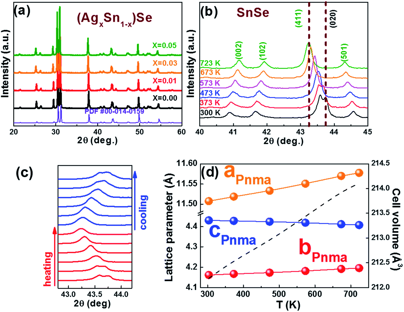 | ||
| Fig. 4 (a) Powder XRD patterns of (AgxSn1−x)Se for x = 0, 0.01, 0.03, and 0.05. (b) The temperature dependence of XRD pattern of pristine SnSe nanocrystals. (c) In situ XRD of thermal cycles between 300 to 723 K: red and blue lines corresponding to heating and cooling cycles respectively. (d) Temperature dependence of lattice parameters and cell volume of pristine SnSe nanocrystals are represented by solid lines and dash line, respectively. | ||
3.2 Thermoelectric properties
The thermoelectric properties of all (AgxSn1−x)Se (0 ≤ x ≤ 0.05) nanoplatelet composites were measured by heating and cooling between 300 to 850 K (Fig. 5). Since the anisotropic character is also reflected on the thermoelectric properties, two different measured directions were examined. For clarity in the following discussions only results measured along the direction perpendicular to the SPS pressing directions are shown. Fig. 5a shows the temperature dependence of electrical conductivity, revealing the value increase significantly with Ag contents. With increasing temperature, the electrical conductivity first increased and reached a maximum value near 500 K, then decreased up to 670 K, and increased again. Interestingly, this unique electrical transport behavior is quite similar to that observed in Ag doped PbTe, SnS, and PbS nanocomposites,29–32 which were confirmed as a combination of grain-boundary potential barrier scattering and phonon scattering processes. The possible reason may be related to the chemisorption or precipitates on the surface of grains, which would form energy barriers and hinder the conduction of carriers between grains.30,31 As the temperature increases, the average energy of the carriers will be sufficient to overcome this energy barrier and hence leads to an increase in the electrical conductivity. However, at high temperatures, the transport process of the carriers is generally limited by acoustic phonon scattering. Meanwhile, the electrical conductivity of the in-plane direction (perpendicular to the SPS pressing direction) is about 75–60% (300–850 K) higher than the other direction, showing an obvious anisotropic behaviour (see ESI Fig. S3†). At 300 K, the electrical conductivity of n doped SnSe is comparable to that of 1% Ag doped SnSe hot pressed ingot of C. L. Chen et al.12 Upon doping with Ag elements, σ is enhanced markedly from 1112 S m−1 to 1903 S m−1 along with a decrease of S from 198 μV K−1 to 123 μV K−1 (Fig. 5b). The result is in good agreement with the increase of carrier concentration, and evidenced by the Hall measurement results at 300 K for all samples listed in Table 1. The temperature dependence of Seebeck coefficients exhibit p-type character with holes as the dominant carriers (Fig. 5b). Moreover, the occurrence of a maximum in the Seebeck coefficient implies a contribution of bipolar effect in these samples. The maximum Seebeck coefficient of pristine SnSe composite is approximately 321 μV K−1 at 700 K. The gradual decrease in Seebeck coefficient with increasing Ag dopants is consistent with the increase of Hall carrier concentration (Table 1). A high power factor (PF) of about 634 μW m−1 K−2 was obtained in the 3% Ag doped sample at 850 K, which is 30–40% higher than the pristine SnSe composite (Fig. 5c).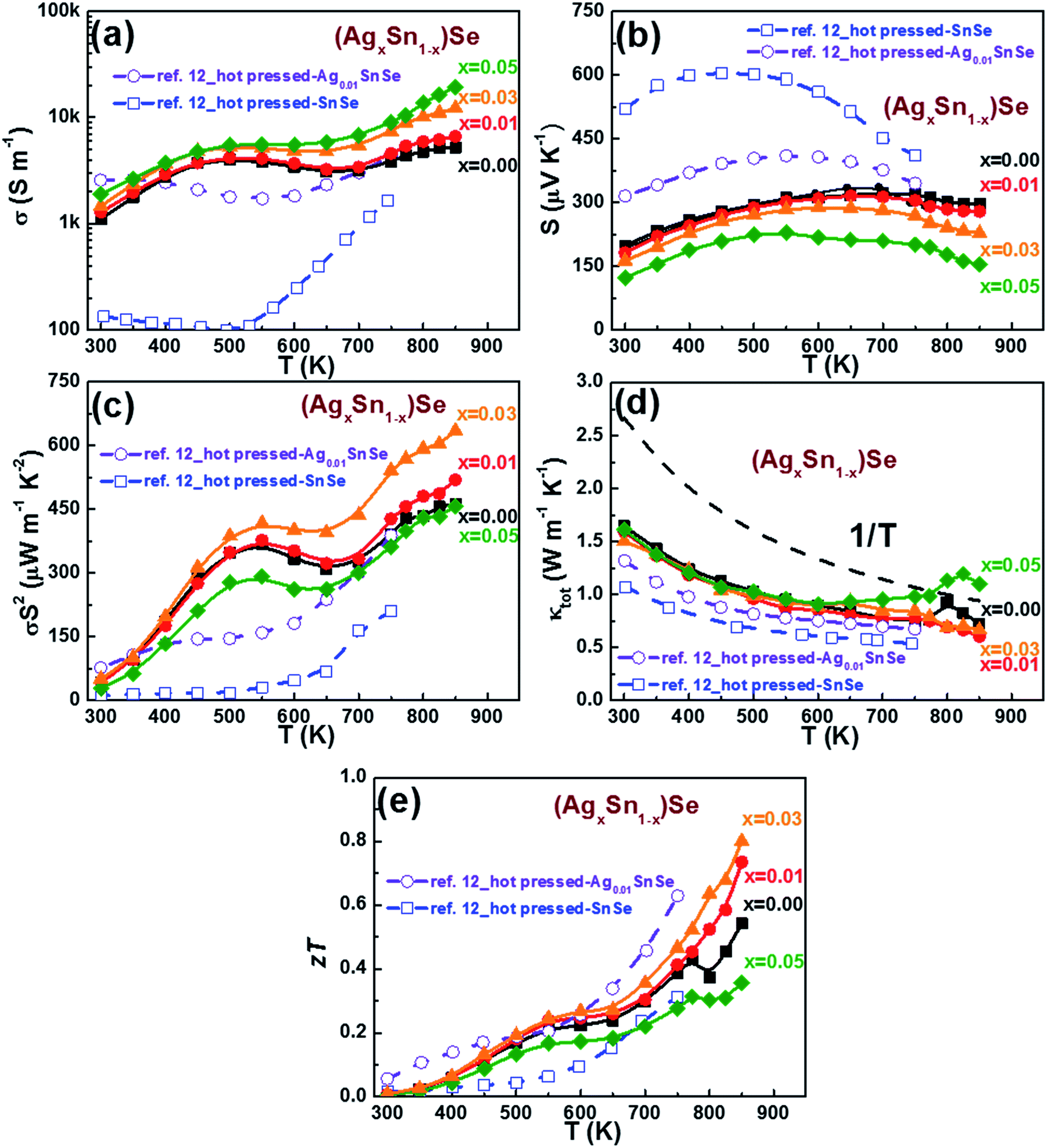 | ||
| Fig. 5 Temperature dependence of (a) electrical conductivity, (b) Seebeck coefficient, (c) power factor, (d) total thermal conductivity, and (e) zT of (AgxSn1−x)Se for x = 0, 0.01, 0.03, and 0.05, measured along the direction perpendicular to the SPS press direction. The polycrystal Ag0.01SnSe and SnSe measured along the same direction to SPS press direction by C. L. Chen et al. are represented by purple by solid lines and green open symbols respectively for comparisons.12 | ||
| Nominal composition | EDX composition | nH (1018 cm−3) | μ (cm2 V−1 s−1) | σ (S m−1) | S (μV K−1) | κtot (W m−1 K−1) |
|---|---|---|---|---|---|---|
| SnSe | Sn0.96Se1.04 | 0.5 | 139 | 1112 | 198 | 1.71 |
| (Ag0.01Sn0.99)Se | Ag0.015Sn0.955Se1.03 | 1.2 | 67 | 1284 | 182 | 1.63 |
| (Ag0.03Sn0.97)Se | Ag0.03Sn0.93Se1.04 | 5.2 | 18 | 1462 | 163 | 1.55 |
| (Ag0.05Sn0.95)Se | Ag0.051Sn0.909Se1.04 | 9 | 13 | 1903 | 123 | 1.67 |
The temperature dependence of thermal conductivity (κtot) is shown in Fig. 5d. It is obvious that the thermal conductivity decreases with increasing temperature until ∼750 K. It is noticed that the Cp has an upturn near 800 K, which is related to the structural phase transition at this temperature (see ESI Fig. S4†). The conclusion also agrees with the reported results by Q. Zhang et al. and S. Sassi et al.23,33 Consequently the observed upturn of κtot at ∼800 K is attributed to the abovementioned structural phase transition from Pnma to Cmcm. The total thermal conductivity κtot is the combination of the electronic contribution κe and the lattice contribution κlat. The κe was evaluated from the Wiedemann Franz relation: κe = σLT, where σ, L and T are the electrical conductivity, Lorenz number, and absolute temperature, respectively. By fitting the Seebeck coefficient data to the reduced chemical potential, a Lorenz number, L of 1.6 × 10⁻⁸ V2 K−2 is obtained. The κlat is then obtained by subtracting κe from κtot. Because of the low electrical conductivity in these samples, the electronic contribution are almost negligible. The measured κtot practically reflects the change of lattice thermal conductivity with temperature. No significant dependency between κtot and doping level is observed at temperature below 600 K. Moreover, κtot for all samples decreases with temperature increase, and approximately follows the 1/T fitting. The dominance of the Umklapp phonon scattering process is proposed to explain such low lattice thermal conductivities in (AgxSn1−x)Se nanocomposites.34
The temperature dependence of zT for (AgxSn1−x)Se nanocomposites are shown in Fig. 5e. The zT of the 3% Ag doped sample reaches a maximum value of 0.8 at 850 K, showing an approximately 40% enhancement over the pristine sample. Continuously increasing carrier concentration with increase of Ag content did not further increase zT. This is because of the lower Seebeck coefficient and the higher thermal conductivity. An appropriate Ag doping is essential to maximize zT by optimizing the electrical and thermal conductivity.
4. Conclusions
Nanocrystals of (AgxSn1−x)Se (0 ≤ x ≤ 0.05) were successfully prepared by a facile, surfactant-free, and cost-effective way, and pressed into dense pellets by spark plasma sintering. The crystal growth process and mechanism of SnSe nanocrystals were investigated through in-depth microstructure analysis. The atomic bonding and surface energy play important roles in the formation of nanocrystals. Furthermore, the dynamic structural behaviour of nanocrystals was investigated by in situ temperature dependent XRD. With Ag doping, the carrier concentration can be effectively enhanced from 0.5 × 1018 cm−3 to 9 × 1018 cm−3. We found 3% Ag doping shows a maximum zT of 0.8 at 850 K, showing an approximately 40% enhancement over the pristine SnSe. The zT enhancement of Ag doped alloys is mainly attributed the enhanced power factor and slightly decrease of thermal conductivity at high temperature region of T > 750 K.Acknowledgements
This work is financially supported by Ministry of Science and Technology (MOST), Taiwan, Grant No. MOST 105-2119-M-001-008.References
- L. E. Bell, Science, 2008, 321, 1457 CrossRef CAS PubMed
.
- G. J. Snyder and E. S. Toberer, Nat. Mater., 2008, 7, 105 CrossRef CAS PubMed
- Y. Z. Pei, X. Y. Shi, A. LaLonde, H. Wang, L. D. Chen and G. J. Snyder, Nature, 2011, 473, 66 CrossRef CAS PubMed
- K. Biswas, J. Q. He, I. D. Blum, C. I. Wu, T. P. Hogan, D. N. Seidman, V. P. Dravid and M. G. Kanatzidis, Nature, 2012, 489, 414 CrossRef CAS PubMed
- B. Poudel, Q. Hao, Y. Ma, Y. C. Lan, A. Minnich, B. Yu, X. A. Yan, D. Z. Wang, A. Muto, D. Vashaee, X. Y. Chen, J. M. Liu, M. S. Dresselhaus, G. Chen and Z. F. Ren, Science, 2008, 320, 634 CrossRef CAS PubMed
- L. D. Zhao, S. H. Lo, Y. S. Zhang, H. Sun, G. J. Tan, C. Uher, C. Wolverton, V. P. Dravid and M. G. Kanatzidis, Nature, 2014, 508, 373 CrossRef CAS PubMed
- R. He, L. H. Huang, Y. M. Wang, G. Samsonidze, B. Kozinsky, Q. Y. Zhang and Z. F. Ren, APL Mater., 2016, 4, 13576 Search PubMed
- P. C. Wei, S. Bhattacharya, J. He, S. Neeleshwar, R. Podila, Y. Y. Chen and A. M. Rao, Nature, 2016, 539, E1 CrossRef CAS PubMed
- G. Li, U. Aydemir, M. Wood, W. A. Goddard III, P. Zhai, Q. Zhang and G. J. Snyder, Chem. Mater., 2017, 29, 2382 CrossRef CAS
- D. Ibrahim, J. B. Vaney, S. Sassi, C. Candolfi, V. Ohorodniichuk, P. Levinsky, C. Semprimoschnig, A. Dauscher and B. Lenoir, Appl. Phys. Lett., 2017, 110, 032103 CrossRef
- S. T. Lee, M. J. Kim, G. G. Lee, S. G. Kim, S. Lee, W. S. Seo and Y. S. Lim, Curr. Appl. Phys, 2017, 17, 732 CrossRef
- C. L. Chen, H. Wang, Y. Y. Chen, T. Day and G. J. Snyder, J. Mater. Chem. A, 2014, 2, 11171 CAS
- E. K. Chere, Q. Zhang, K. Dahal, F. Cao, J. Mao and Z. Ren, J. Mater. Chem. A, 2016, 4, 1848 CAS
- K. L. Peng, X. Lu, H. Zhan, S. Hui, X. D. Tang, G. W. Wang, J. Y. Dai, C. Uher, G. Y. Wang and X. Y. Zhou, Energy Environ. Sci., 2016, 9, 454 CAS
- L. D. Zhao, G. J. Tan, S. Q. Hao, J. Q. He, Y. L. Pei, H. Chi, H. Wang, S. K. Gong, H. B. Xu, V. P. Dravid, C. Uher, G. J. Snyder, C. Wolverton and M. G. Kanatzidis, Science, 2016, 351, 141 CrossRef CAS PubMed
- Y. X. Chen, Z. H. Ge, M. Yin, D. Feng, X. Q. Huang, W. Zhao and J. He, Adv. Funct. Mater., 2016, 26, 6836 CrossRef CAS
- M. Gharsallah, F. Serrano-Sanchez, N. M. Nemes, F. J. Mompean, J. L. Martinez, M. T. Fernandez-Diaz, F. Elhalouani and J. A. Alonso, Sci. Rep., 2016, 6, 26774 CrossRef CAS PubMed
- T. A. Wubieneh, C. L. Chen, P. C. Wei, S. Y. Chen and Y. Y. Chen, RSC Adv., 2016, 6, 114825 RSC
- Y. J. Fu, J. T. Xu, G. Q. Liu, X. J. Tan, Z. Liu, X. Wang, H. Z Shao, H. C Jiang, B. Liang and J. Jiang, J. Electron. Mater., 2017, 46, 3182 CrossRef CAS
- G. Han, S. R. Popuri, H. F. Greer, L. F. Llin, J. W. G. Bos, W. Zhou, D. J. Paul, H. Ménard, A. R. Knox, A. Montecucco, J. Siviter, E. A. Man, W. G. Li, M. C. Paul, M. Gao, T. Sweet, R. Freer, F. Azough, H. Baig, T. K. Mallick and D. H. Gregory, Adv. Energy Mater., 2017, 1602328 CrossRef
- H. Guo, H. Xin, X. Qin, J. Zhang, D. Li, Y. Li, C. Song and C. Li, J. Alloys Compd., 2016, 689, 87 CrossRef CAS
- G. Tang, W. Wei, J. Zhang, Y. Li, X. Wang, G. Xu, C. Chang, Z. Wang, Y. Du and L. D. Zhao, J. Am. Chem. Soc., 2016, 138, 13647 CrossRef CAS PubMed
- Q. Zhang, E. K. Chere, J. Y. Sun, F. Cao, K. Dahal, S. Chen, G. Chen and Z. F. Ren, Adv. Energy Mater., 2015, 5, 1500360 CrossRef
- Z. H. Ge, K. Y. Wei, H. Lewis, J. Martin and G. S. Nolas, J. Solid State Chem., 2015, 225, 354 CrossRef CAS
- G. Han, S. R. Popuri, H. F. Greer, J. W. G. Bos, W. Z. Zhou, A. R. Knox, A. Montecucco, J. Siviter, E. A. Man, M. Macauley, D. J. Paul, W. G. Li, M. C. Paul, M. Gao, T. Sweet, R. Freer, F. Azough, H. Baig, N. Sellami, T. K. Mallick and D. H. Gregory, Angew. Chem., Int. Ed., 2016, 55, 6433 CrossRef CAS PubMed
- X. H. Ma, K. H. Cho and Y. M. Sung, CrystEngComm, 2014, 16, 5080 RSC
- C. W. Li, J. Hong, A. F. May, D. Bansal, S. Chi, T. Hong, G. Ehlers and O. Delaire, Nat. Phys., 2015, 11, 1063 CrossRef CAS
- D. Bansal, J. W. Hong, C. W. Li, A. F. May, W. Porter, M. Y. Hu, D. L. Abernathy and O. Delaire, Phys. Rev. B, 2016, 94, 054307 CrossRef
- Q. Tan, L. D. Zhao, J. F. Li, C. F. Wu, T. R. Wei, Z. B. Xing and M. G. Kanatzidis, J. Mater. Chem. A, 2014, 2, 17302 CAS
- J. Martin, L. Wang, L. Chen and G. S. Nolas, Phys. Rev. B: Condens. Matter Mater. Phys., 2009, 79, 115311 CrossRef
- Y. Zheng, S. Wang, W. Liu, Z. Yin, H. Li, X. F. Tang and C. Uher, J. Phys. D: Appl. Phys., 2014, 47, 11501 Search PubMed
- Y. W. Li, F. Li, J. F. Dong, Z. H. Ge, F. Y. Kang, J. Q. He, H. D. Du, B. Lia and J. F. Li, J. Mater. Chem. C, 2016, 4, 2047 RSC
- S. Sassi, C. Candolfi, J. B. Vaney, V. Ohorodniichuk, P. Masschelein, A. Dauscher and B. Lenoir, Appl. Phys. Lett., 2014, 104, 212105 CrossRef
- D. R. Clarke, Surf. Coat. Technol., 2003, 163, 67 CrossRef
Footnotes |
| † Electronic supplementary information (ESI) available. See DOI: 10.1039/c7ra05819e |
| ‡ These authors contributed equally to this work. |
| This journal is © The Royal Society of Chemistry 2017 |