
 Open Access Article
 This Open Access Article is licensed under a
 Creative Commons Attribution 3.0 Unported Licence
Strain and electric field tunable electronic structure of buckled bismuthene†
Ming-Yang Liu a,
Yang Huanga,
Qing-Yuan Chena,
Ze-Yu Lia,
Chao Caob and
Yao He*a
a,
Yang Huanga,
Qing-Yuan Chena,
Ze-Yu Lia,
Chao Caob and
Yao He*a
aDepartment of Physics, Yunnan University, Kunming, Yunnan 650091, People's Republic of China. E-mail: yhe@ynu.edu.cn
bDepartment of Physics, Hangzhou Normal University, Hangzhou, Zhejiang 310036, People's Republic of China
First published on 14th August 2017
Abstract
Based on first-principles density functional theory calculations, we systemically study the properties of two-dimensional buckled single-layer bismuth (b-bismuthene). The structure, stability, and electronic properties are mainly discussed by PBE + SOC method and the hybrid functional HSE06 method is used to further revise the band gap. The optimized b-bismuthene is determined to be dynamically and thermally stable with an indirect band gap. In particular, there is a peculiar Rashba spin-splitting emerging in the valence band maximum (VBM) states. Interestingly, the Rashba energy could be effectively modulated by in-layer biaxial strain. By applying in-layer biaxial strain, one can find that b-bismuthene has indirect–direct band gap and semiconductor–semimetal transitions. Moreover, we also study the electronic structure of bilayer b-bismuthene that is sensitively dependent on the interlayer distance. We demonstrate that the electric field (E-field) leads to a breaking of the Rashba-type splitting near the VBM of single b-bismuthene. More importantly, there is a synergistic effect when both strain and electric field are applied at the same time. The E-field induced band splitting character could be modified by the strain strength. Thus, this study indicates that b-bismuthene may be a potential material in both electronic and spintronic devices.
1 Introduction
Two-dimensional (2D) materials have become a favorite in the materials science community due to a flourish of studies in recent years.1,2 Since they possess intriguing properties and differ from their bulk counterparts in various aspects resulting from the confinement effect, 2D materials lead to a surge of interest in both theory and experiment. Following the successful exploration of 2D materials from group IV elements,3–5 it is an attractive prospect to probe into new 2D monolayer materials of group V elements or pnictogens. As expected, the monolayers of group V elements, which are named as nitrogene,6 phosphorene,7,8 arsenene,9–11 and antimonene,10,12 respectively, have been predicted to be dynamically and thermally stable by means of their phonon spectra and ab initio molecular dynamic (AIMD) calculations at finite temperature. In contrast to the unique Dirac cone at the Fermi level in group IV elements, the monolayers of group V elements are insulating or semiconducting (nitrogene is insulator and phosphorene, arsenene, and antimonene are semiconductors) with wide-range fundamental band gap covering from 0.36 to 5.90 eV.6,13–15 Also, the high carrier mobility and anisotropic excitons,16–20 as well as electric field and strain tunable electronic structure,9,10,21–23 are revealed in these 2D pnictogens semiconductors. Particularly, phosphorene field effect transistor and mechanical isolation of highly stable antimonene have been realized in experiment,24,25 recently, which will further promote investigation. As a consequence, these group V elements monolayers may be more excellent than group IV elements in practical electronic and optoelectronic applications.Although many efforts have been devoted to the 2D pnictogens materials, the freestanding single-layer bismuth preserves almost unexplored. Quite recently, as the heaviest element of pnictogens, the freestanding single-layer bismuth derived from bulk form, namely bismuthene, has been proposed that it is stable at high temperature and shows fascinating electronic properties.26 In fact, there has been a considerable focus on bismuth for many years due to the peculiar semimetal character and strong spin–orbit coupling (SOC).27–32 Similar to the gray arsenic and gray antimony, metallic bismuth is the rhombohedral A7 structure with space group R![[3 with combining macron]](https://www.rsc.org/images/entities/char_0033_0304.gif) m and can also be described as a hexagonal structure. It is well known that the size effects and surfaces are crucial for the physical properties of materials, thus the ultrathin films and surfaces of bismuth are widely studied in previous works. On one hand, the intrinsic strong SOC induced a strong Rashba-type spin splitting of the surfaces-state bands on surfaces of bismuth is exposed;29 on the other hand, the ultrathin Bi films have an intimate relationship with respect to the quantum spin Hall (QSH) effects.31,33 For instance, a single bilayer (BL) Bi (111) film is predicted to be an elemental 2D topological insulator (TI)31,34 and the Bi (111) films with stable 2D TI phase are independent of the film thickness.33 Meanwhile, the 2D TI states are robust in BL-Bi film against strain and electric field.35 Interestingly, a giant gap QSH and mysterious valley-polarized quantum anomalous Hall states emerge as the Bi films are functionalized by hydrogen,36 which may initiate more searches for novel properties of Bi films.
m and can also be described as a hexagonal structure. It is well known that the size effects and surfaces are crucial for the physical properties of materials, thus the ultrathin films and surfaces of bismuth are widely studied in previous works. On one hand, the intrinsic strong SOC induced a strong Rashba-type spin splitting of the surfaces-state bands on surfaces of bismuth is exposed;29 on the other hand, the ultrathin Bi films have an intimate relationship with respect to the quantum spin Hall (QSH) effects.31,33 For instance, a single bilayer (BL) Bi (111) film is predicted to be an elemental 2D topological insulator (TI)31,34 and the Bi (111) films with stable 2D TI phase are independent of the film thickness.33 Meanwhile, the 2D TI states are robust in BL-Bi film against strain and electric field.35 Interestingly, a giant gap QSH and mysterious valley-polarized quantum anomalous Hall states emerge as the Bi films are functionalized by hydrogen,36 which may initiate more searches for novel properties of Bi films.
For the freestanding 2D single-layer, a promising route for tuning the electronic structure is by applying strain and external electric field. It has been found that strain and electric field can lead to the semiconductor–metal, semiconductor–semimetal, and trivial-to-topological transitions as well as other various features in monoelemental pnictogens materials and group-V-V 2D semiconductors.9–11,21–23,37–39 Actually, strain and electric field effects are inevitable for the 2D materials in practical application, which can be induced by substrate and interfacial charge transfer. These situations have been explicitly demonstrated by means of emerging a strain-induced topological transition of ultrathin Bi (111) films grown on Bi2Te3 (111) substrates40 and creating helical Dirac fermion state of a single BL-Bi grown on a single quintuple layer Bi2Se3 or Bi2Te3 because of interfacial charge transfer.41 However, the electronic structure of the new suspended bismuthene is still devoid of tuning by strain and electronic field to the best of our knowledge even though the single and bilayer bismuthene have been systemically studied in stability, mechanical and electronic properties, recently.26 Specific exploration of the strain and electric field tuned bismuthene can render comprehensive understanding of the bismuthene employing in practical application. Therefore, it is urgent to study the properties of the strain and electric field tuned bismuthene.
In this paper, we systemically study the stability and electronic structure of strain and electric field (E-field) tuned buckled bismuthene (b-bismuthene) phase using PBE + SOC method. The hybrid functional HSE06 method is used to further revise the band gap. The optimized b-bismuthene is determined to be dynamically and thermally stable with indirect band gap. In particular, there is a peculiar Rashba spin-splitting emerging in the valence band maximum (VBM) states. Interestingly, the Rashba energy could be effectively modulated by the in-layer biaxial strain. By applying the in-layer biaxial strain, one can find that b-bismuthene has indirect–direct band gap and semiconductor–semimetal transitions. Moreover, we also study the electronic structure of bilayer b-bismuthene that is sensitively dependent on the interlayer distance. We demonstrate that the electric field leads to a breaking Rashba-type splitting near the VBM of single b-bismuthene. Importantly, there is a synergy effect when both strain and electric field are applied at same time. The E-field induced band splitting character could be tuned by the strain strength. Our findings indicate that b-bismuthene could be a promising candidate for the electronic and spintronic materials in the future.
2 Methods
The first-principles calculations were based on density functional theory (DFT) using the Vienna Ab Initio Simulation Package (VASP).42 We employed the Perdew–Burke–Ernzerhof (PBE) generalized gradient approximation (GGA)43 including spin–orbit coupling (SOC) for the exchange correlation interaction. The cut off energy of 500 eV was used for the plane wave basis. A 21 × 21 × 1 k-grid mesh in the Brillouin zone of the unit cell was adopted for the 2D bismuthene nanosheets, and a vacuum of about 20 Å was introduced to avoid interaction between periodic images of slabs in the z direction. To obtain a more precise band gap, the screened hybrid functional method44 in HSE06 level including SOC is also used, and the k-grid mesh in the Brillouin zone of the unit cell is changed to be 12 × 12 × 1. We took into account the van der Waals (vdW) correction PBE-D2 functional45 in bilayer bismuthene to explore the effects of vdW forces. For ionic relaxations, the convergence criterion between two consecutive steps in our self-consistent calculations was 10−5 eV, and the criteria for the forces during the ionic relaxation was 0.01 eV Å−1. Furthermore, the phonon dispersion and ab initio molecular dynamics (AIMD) simulation are performed to check the dynamical and room temperature thermal stabilities. For the AIMD simulation, we used 4 × 4 × 1 supercell and the temperature of 300 K, and the total simulation time was 3 ps with a time step of 3 fs.3 Results and discussion
3.1 Atomic structure and stabilities of 3D bismuth and bismuthene
Our discussion will start from the calculations of 3D bismuth crystal. As Introduction mentioned above, bulk bismuth belongs to the rhombohedral A7 structure and space group Rm, each atom bonds covalently to its three nearest neighbors forming buckled bilayer with σ bond as the general character of pnictogens semimetal. The interaction between the adjacent bilayer is much weaker than the inter-bilayer bonding, thus it can be realized that bulk bismuth cleaves along the (111) plane.32 Based on these understandings, we optimize the structure of bulk bismuth using PBE and PBE + SOC methods. It is clearly suggested that including SOC obviously increases the lattice constants, as list in Tables S1† and 1, which means that SOC should be worthy of consideration in the structure relaxation. We also compare our results to the recent work ref. 26, showing a good agreement. Furthermore, the anisotropy of 3D bismuth crystal using optimized structural parameters is calculated on account of the existence of out-of-pane and in-plane interatomic distances. The anisotropy is obtained by the expression:
 | (1) |
We find that the anisotropy of PBE optimized structure is evidently smaller than PBE + SOC, indicating SOC plays an important role for studying the anisotropy of bulk bismuth. For the electronic structure, the calculated direct and indirect band gaps with SOC are 53 and −111 meV, respectively. These two values are consistent with recent work.26
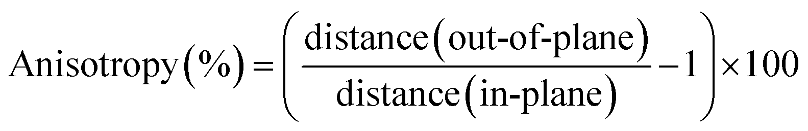
Now, we turn to discuss the structure and stability of single b-bismuthene. In analogy with buckled arsenene and antimonene, b-bismuthene has a 2D buckled honeycomb structure with two Bi atoms in the primitive unit cell, which is similar to the previously proposed BL-Bi (111) structure, as illustrated in Fig. 1(a). In the b-bismuthene, three electrons of each Bi atom bond covalently to the three nearest neighbors forming three strong σ-like bonds. The rest of lone pair electrons contribute the π-like bond between two Bi atoms in the primitive unit cell, alternately in an upper and a lower plane, resulting in a pseudo-Jahn–Teller distortion.46 In order to enhance the stability, the sp3-type hybridization replaces the planar sp2-type hybridization by means of producing the buckling. The same mechanism has also been represented in b-arsenene and b-antimonene which share the similar buckled configuration.10,12 The optimized structural parameters and other relative values are summarized in Table 2 and S2,† one can see that, similar to bulk bismuth, SOC leads to an obvious increase of the lattice constant, i.e., changing from 4.33 to 4.39 Å. However, not only the lattice constant but also the bond length and bond angle, they decrease evidently when the b-bismuthene is cleaved from the bulk bismuth due to the quantum confinement effect. We also notice that the buckling height of b-bismuthene is larger than that of the bulk bismuth, which can be attributed to the disappearance of the interlayer coupling. Moreover, from b-nitrogene to b-bismuthene, the buckling height increases from 0.7 to 1.73 Å. This is in line with the fact that the atomic radius has a gradual reduction from Bi to N atoms.
 | ||
| Fig. 1 Calculated results of single b-bismuthene using PBE + SOC method. (a) Top and side views of the optimized atomic configuration and structural parameters. (b) Phonon dispersion spectrum with PBE + SOC optimized parameters. (c) Band structure, density of states, and Frontier states character of single b-bismuthene. The energy range 0.2 eV below the top of the valence band is green shaded in the band structure and density of states. The band gap is depicted by red range. ER is the Rashba energy. | ||
Next we calculate the cohesive energy, phonon dispersive spectrum, and AIMD to check the stability and experimental feasibility of the b-bismuthene phase. The cohesive energy is calculated by
| Ec = (nEatom − Ebismuthene)/n, | (2) |
According to the recent experiment reports,25 the highly stable b-antimonene can be fabricated through mechanical isolation. Whether b-bismuthene can also exfoliate from its bulk form, it is therefore a significant question. To address this question, we calculate the interaction energies of layered bismuth by considering vdW correction PBE-D2 functional. Interestingly, the calculated interaction energies are 123 meV per atom for the layered bismuth. This value is slightly larger than that of layered antimony (86 meV per atom)10 and twice larger than that of graphite (63.5 meV per atom).49 On the other hand, the cohesive energies differences between the free b-bismuthene and the 3D bismuth are very small (only 0.12 eV per atom), which indicates a possible formation. Therefore, it is worth expecting that b-bismuthene may be fabricated by the same exfoliation method.
3.2 The electronic structure of b-bismuthene tuned by in-layer biaxial strain
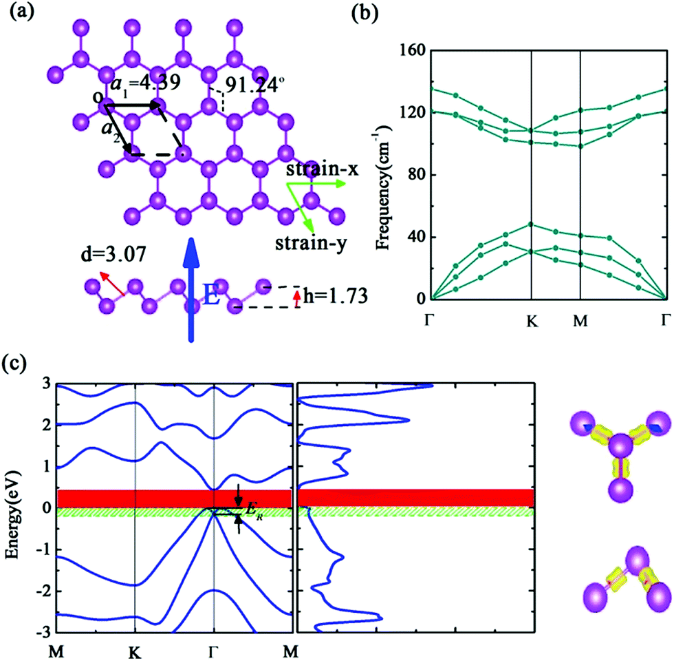
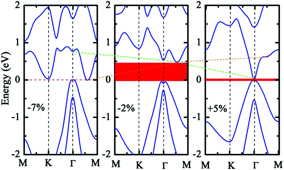
The results of the geometric structure optimization have indicated that SOC should not be neglected for the study of b-bismuthene. Hence here, the electronic structure calculations are mainly discussed by PBE + SOC method. The results using PBE method are presented in ESI.† As seen in Fig. 1(c), SOC splits the double degenerate bands for each spin channel of VBM, showing a distinct Rashba-type splitting because of the perpendicular potential asymmetry. The splitting two branches intersect, forming a Dirac point and displaying a Mexican-hat shape near the VBM. The Rashba energy ER that is the energy difference between the crossing point and the band edge is calculated to be 133 meV. This value is slightly larger than that of BiTeI (ER = 113 meV) material,50 implying a strong Rashba effect. These intriguing characters also are proposed in the tetragonal bismuth bilayer that is predicted as a stable and robust quantum spin hall insulator.51 The 2D Bi (111) structure in fact as a TI has been discussed intensively in ref. 31, 33, and 34. Accordingly, this Rashba-type splitting of b-bismuthene is of special importance for fabricating spintronic devices. In contrast, the VBM is shifted from the Γ to the Γ–M and Γ–K directions by ∼1/6 of the Γ–M and Γ–K distances resulting from the Rashba-type splitting, and the band gap decreases to 0.46 eV. When the vdW correction is considered, the band gap retains nearly unchanged and is similar to the case of without SOC. Nevertheless, the SOC gap decreases slightly under HSE06 level. Even if SOC affects the band shape of b-bismuthene significantly, the Frontier states of VBM retain the robust σ-like bond (see Fig. 1(c) and S1(c)†). Our calculated electronic structure of b-bismuthene with SOC is in good agreement with the previous works.26,35Normally, structure deformation induced by substrates and external environment always is inevitable in practical applications, which has a prominent influence on the physical properties of materials. These have been demonstrated in 2D single-layer materials, for instance graphene, phosphorene, arsenene, and antimonene. Here we study the strain-tuned b-bismuthene with SOC to mimic the structure deformation. The in-layer biaxial strain ε is expressed as ε = (a − a0)/a0, where a0 is the lattice constant of the free b-bismuthene. The discussed strain range −10% ≤ ε ≤ +10% is relatively feasible in experiment, since b-bismuthene possesses a lager buckling height. As shown in Fig. 2, there is an interesting finding that the band structure is very sensitive to the applied in-layer biaxial strain ε. For example, a smaller compressive strain −2% can induce the CBM changing from the Γ high symmetry point to the Γ–M direction. Notably, two bands near the VBM emerge an evident splitting and the Mexican-hat shape tends to flatness on account of a smaller strain exerted. This phenomenon is consistent with the previous study.35 Moreover, we find that the splitting of the two bands near the VBM gradually widens with the strain increasing, which means that the in-layer biaxial strain ε can enhance the band splitting. In particular, b-bismuthene is altered to a direct band gap under +5% tensile strain due to the Mexican-hat disappearance at the Γ high symmetry point. Analogous to PBE level (see ESI†), the −7% compressed strain transforms b-bismuthene into semimetal. The band shape and electronic phase variations with strain offer a reason to explore whether the Rashba energy ER can be affected by exerting strain. As depicted in Fig. 3(a), the variation picture of the Rashba energy ER exhibits a ‘W’-like shape with the strain ranging from −10% to +10%. That is, the strain is an effective way to modulate the Rashba effect of b-bismuthene, which originates from the intrinsic buckling structure of b-bismuthene compressed and stretched by strain, inducing the change of inversion symmetry. Strain-tunable Rashba energy may be useful to the b-bismuthene applying to spintronic devices without external magnetic field.
 | ||
| Fig. 2 Calculated band structure of −7%, −2% and +5% strains under PBE + SOC level. | ||
 | ||
| Fig. 3 Strain dependence of (a) the Rashba energy ER, (b) the band gap Eg using PBE + SOC method. The insets ‘M’, ‘ID’, and ‘D’ represent metallic, indirect, and direct characters, respectively. (c) Strain dependence of the band gap Eg by using HSE06 + SOC method. | ||
The band gap of b-bismuthene as a function of in-layer strain ε under PBE + SOC level is presented in Fig. 3(b). One can see that the variation of band gap is sensitive to smaller strain, showing an ‘N’-like shape. The largest gap value occurs at ε = −1% with Eg = 0.52 eV, which is also found in ref. 35. As mentioned above, a special strain is the ε = +5% that results in an indirect–direct transition, but the direct gap can return quickly to be indirect with the strain increasing. It should be mentioned that, at +6% ≤ ε ≤ +10%, the band gap is proportional to the ε, which is opposite to the case of without SOC (see ESI†). So our results demonstrate that, under PBE + SOC level, the electronic structure of b-bismuthene is tunable with respect to a certain range of in-layer biaxial strain. The band gap is further calculated using HSE06 + SOC method, as shown in Fig. 3(c). Although HSE06 revises the gap values, the variation trend is approximately identical to the PBE level. We notice that the mismatch of lattice constants between b-bismuthene and Bi2Se3 or Bi2Te3 is about −6% and 0, which is a similar effect for single layer bismuth strained by −6% and 0, respectively. Interestingly, the calculated band gaps using HSE06 + SOC method with −6% and 0 strains are nearly consistent of single b-bismuthene strained by the bulk Bi2Se3 and Bi2Te3 substrates.41 This means that the results in present work could agree with the experimental reports and the strain tunable electronic structure of b-bismuthene may be realized in real systems by growing on appropriate substrates.
3.3 Bilayer b-bismuthene affected by interlayer distance
Stacking 2D materials is an attractive subject in materials science study. Novel electronic structures in phosphorene and arsenene thin films modified by strain and electric field have been reported.11,22 In practical, the interlayer distance also is an important ingredient for physical description of the properties of 2D thin films. Tuning the interlayer distance is analogous to apply the strain along z-direction. In this section, we explore the effects of interlayer distance for bilayer b-bismuthene. Similar to the discussion above, PBE + SOC method is employed. Recent study has pointed that the AA-stacking bilayer is the most stable configuration for b-bismuthene,26 and thus we here only discuss the AA-stacking bilayer b-bismuthene. Our geometric optimization of bilayer b-bismuthene includes the vdW correction using PBE-D2 functional, since the PBE-D2 functional performs best in bulk and few-layer phosphorus in terms of energetics and geometry.52 As seen in Fig. 4(a), the optimized interlayer distance is d1 = 4.64 Å, which is smaller than that of ref. 26 4.80 Å because of including vdW correction. The band structure of AA-stacking bilayer b-bismuthene is plot in Fig. 4(b). It is noted that, in contrast to single layer b-bismuthene, the Fermi level crosses the VBM and CBM showing a semimetal character due to the interlayer coupling. Therefore, stacking is an effective route to modify the characters of b-bismuthene, such as semiconducting–semimetallic transition, even only constructing bilayer b-bismuthene. Furthermore, the interlayer cohesive energies calculated by PBE + SOC with vdW correction is 0.17 eV per atom, which is noticeably larger than the typical values of vdW bond, and thus the interlayer cohesive energies should be composed of chemical and vdW interactions. This value also implies that bilayer b-bismuthene is energetically feasible.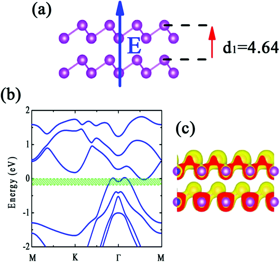 | ||
| Fig. 4 (a) Side view of the optimized atomic configuration, (b) calculated band structure, and (c) Frontier states character of the AA-stacking bilayer b-bismuthene under PBE + SOC level. The energy range 0.2 eV below the top of the valence band is green shaded in the band structure. The band gap is depicted by red range. | ||
The favorable interlayer distance is easily affected by external environment and experiment process, and therefore it is necessary for bilayer b-bismuthene to discuss the relationship between physical properties and interlayer distance. We first examine the dependence relationship between the interlayer cohesive energy and the interlayer distance, as plot in Fig. 5(a). It is shown that both PBE and PBE + SOC methods have a same variation trend and the magnitude of the interlayer cohesive energy decreases as the interlayer distance changes from the equilibrium value. But, bilayer b-bismuthene is still feasible energetically even Δd = 1.5 Å. In particular, the interlayer cohesive energy enters into the vdW energy range when the interlayer distance varies beyond ∼1.0 Å (Δd > 1.0 Å), since the long-range attractive potential controls the vdW interaction between two b-bismuthene layers.
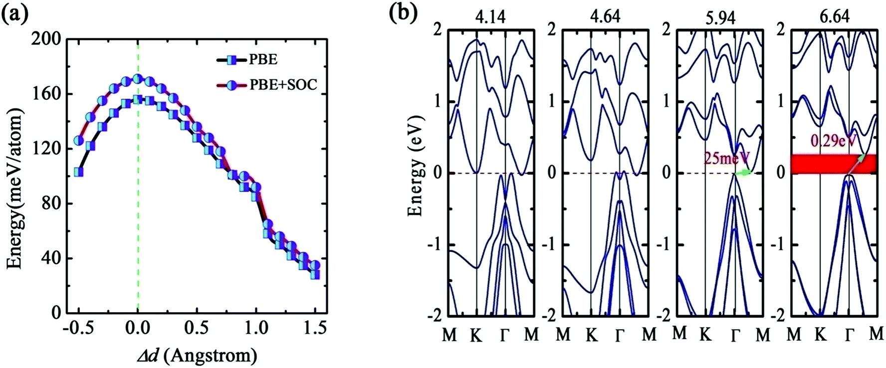 | ||
| Fig. 5 (a) Interlayer distance dependence of the interlayer cohesive energies by PBE level with and without SOC. (b) Band structure of bilayer b-bismuthene with four typical interlayer distances 4.14, 4.64, 5.94, and 6.64 Å using PBE + SOC method. | ||
We next discuss the evolution of the band structure with the interlayer distance, as suggested in Fig. 5(b). Bilayer b-bismuthene can persist the semimetal character until the interlayer distance d1 = 5.94 Å. As the interlayer distance d1 = 5.94 and 6.64 Å, bilayer b-bismuthene becomes an indirect band gap semiconductor with Eg = 0.025 and 0.29 eV. Moreover, we observe that the band shape of VBM is also dependent on the interlayer distance. The Mexican-hat shape disappears when the interlayer distance adds up to a large value (see Fig. 5(b)), since the large interlayer distance weakens the interlayer coupling of bilayer b-bismuthene. As investigated above, the band shape of VBM with SOC corresponds to the Rashba effect, and thus the interlayer distance can mediate the Rashba effect of bilayer b-bismuthene. Based on these discussions, we emphasize that tuning the interlayer distance is useful to enrich the electronic properties and enlarge the application of bilayer b-bismuthene.
3.4 Single and bilayer b-bismuthene tuned by electric field
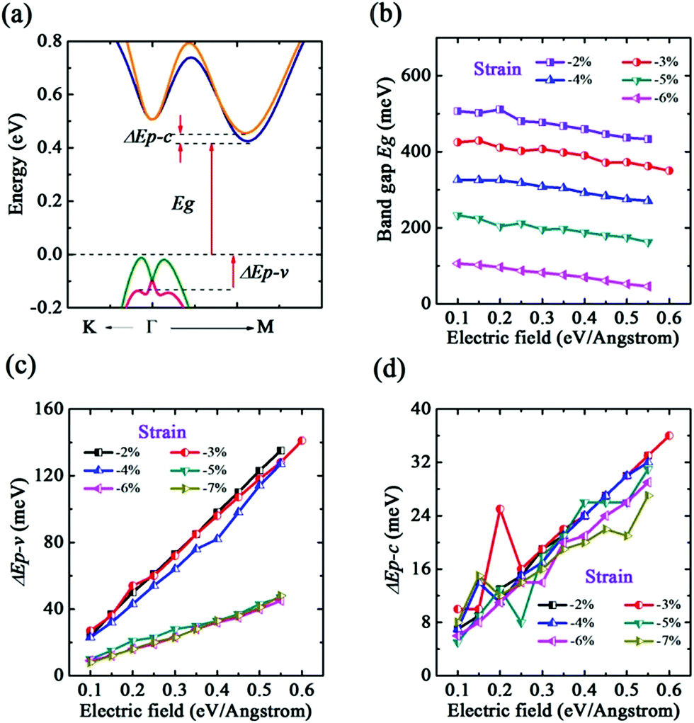
In the b-bismuthene, the existence of buckling gives rise to a potential difference between two atomic layers, which turns out to be possible to provide an intrinsic advantage in tuning the electronic structure in terms of a perpendicular electric field (E-field).22 The E-field applying to single and bilayer b-bismuthene is also a reasonable method to mimic the interfacial charge transfer effect when the single and bilayer b-bismuthene grow on appropriate substrate.35 We perform the calculations with the strength of E-field ranging from −0.60 to 0.60 eV Å−1. A quite interesting finding is that the E-field results in the band spin-degeneracy splitting near the VBM, while the CBM maintains the band spin-degeneracy and is located at the Γ high symmetry point, as presented in Fig. 6(a). This novel electronic structure is since the E-field breaks the Rashba-type splitting induced by inversion symmetry.35,41 In reality, given that b-bismuthene is a centrosymmetric crystal, in which each individual band has double degeneracy for the spin degrees of freedom even though SOC is taken into account. But, the external E-field or substrate can effectively break the inversion symmetry of b-bismuthene, which leads to the band spin-degeneracy splitting and reduces the band gap. The band gap as a function of the E-field is shown in Fig. 6(b). It is suggested that the band gap decreases monotonically with the strength of the E-field. But, the reduction is relatively small from 0.00 to 0.55 eV Å−1. A sharp decrease of the band gap is found as the E-field beyond 0.58 eV Å−1. With a critical E-field Ec = 0.59 eV Å−1 is applied, yielding the semiconductor–metal transition. This critical value is larger 0.02 eV Å−1 than that of without SOC (see ESI†). Indeed, further increasing the E-field to as high as ∼1 eV Å−1 will create the helical Dirac fermions due to a giant Rashba effect, which is similar to BL-Bi grown on Bi2Se3 and Bi2Te3 substrates.41 Moreover, in contrast to the buckled arsenene, the direct-indirect band gap transition cannot be found in single b-bismuthene. In reality, this critical E-field Ec of inducing electronic phase transition are difficult to realize in experiment, and therefore single b-bismuthene may be electric robustness. Furthermore, we also find that, both Eg and ΔEp, the variation trend of applying negative value of E-field is hardly altered, only the value of Ec slightly becomes larger. In contrary to the band gap, the splitting energy ΔEp increases monotonically with the strength of the electric field before the electronic phase transition (see Fig. 6(b)). The largest ΔEp is calculated to be 152 meV at 0.58 eV Å−1.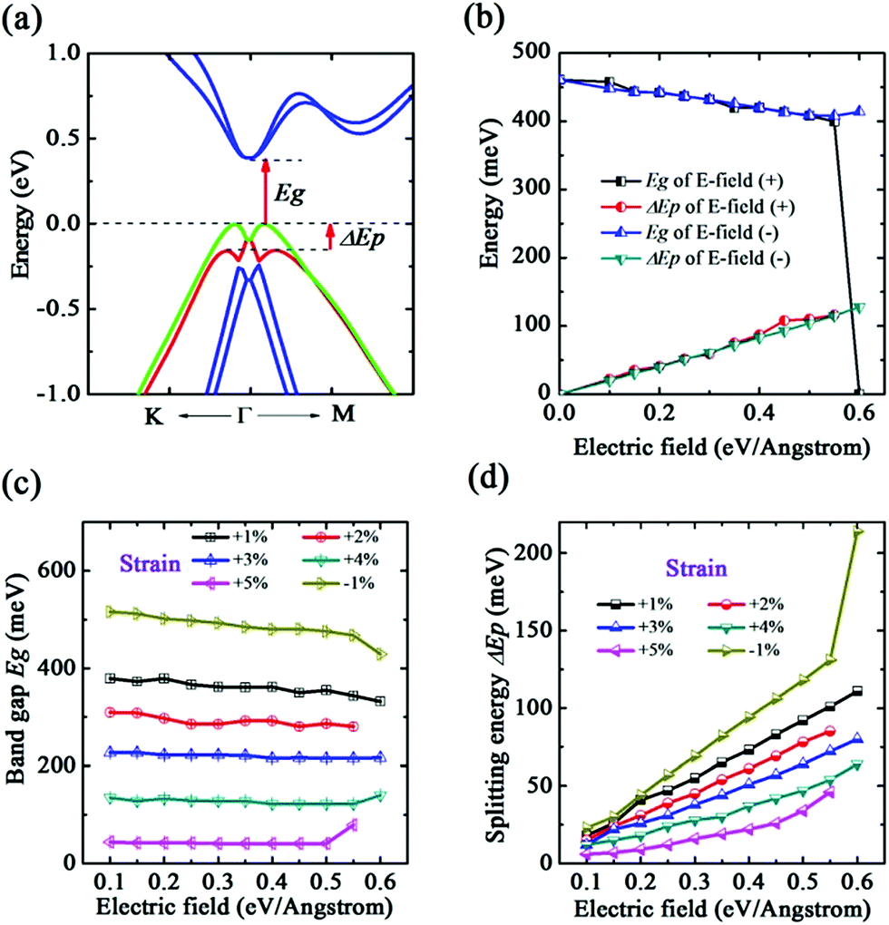 | ||
| Fig. 6 (a) E-Field induced band splitting along K–Γ–M direction. (b) E-Field dependences of the band gap Eg and splitting energy ΔEp of single b-bismuthene. E-Field dependences of (c) the band gap Eg and (d) splitting energy ΔEp with different strains. | ||
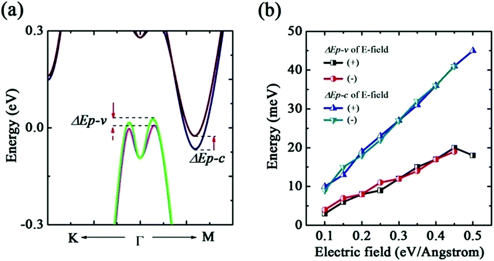
Previous work has demonstrated that if strain and E-field coexist, intriguing electronic properties would be produced in silicon nanowires.53 Motivated by this, we want to know whether there is a synergy effect when both strain and E-field are applied at same time. The strain ε range is considered from −7% to +10%. Because of the similar effect of positive and negative value of E-field, we only apply the positive value of E-field to the b-bismuthene. It is found that when ε is in the range of −1% to +5%, the E-field inducing band splitting is similar to the ε = 0. E-Field dependences of the band gap Eg and splitting energy ΔEp with different strains are depicted in Fig. 6(c) and (d). One can see that the variation curve of Eg and ΔEp with different E-field value is also similar to the ε = 0. Furthermore, under a same E-field value, Eg decreases and ΔEp increases with ε from −1% to +5%.
Interestingly, as shown in Fig. 7(a), the degeneracy of the conduction band near the Γ high symmetry point breaks down at ε = +6% and a band splitting appears in the CBM. Moreover, we notice that the band spin-splitting shape of the VBM is different from ε in the range of −1% to +5%, which could be attributed to the change of band Frontier feature. Thus, this interesting finding indicates the synergy effect emerging when the tensile strain is larger than +5%. We further calculated the band gap and splitting energy of CBM and VBM (ΔEp–c and ΔEp–v). From Fig. 7(b), it is suggested that E-field could slightly modify the band gap, and in contrary to ε in −1% to +5%, Eg increases with the strain. Comparing to the slight change of Eg, both ΔEp–c and ΔEp–v have an obvious modification by increasing E-field, as plot in Fig. 7(c) and (d). It should be mentioned that, under a same value of E-field, ΔEp–v is altered evidently from +6% to +8% while the difference of ΔEp–c between different strains is relatively smaller. That is, the E-field inducing valence band spin-splitting ΔEp–v is more sensitive to strain.
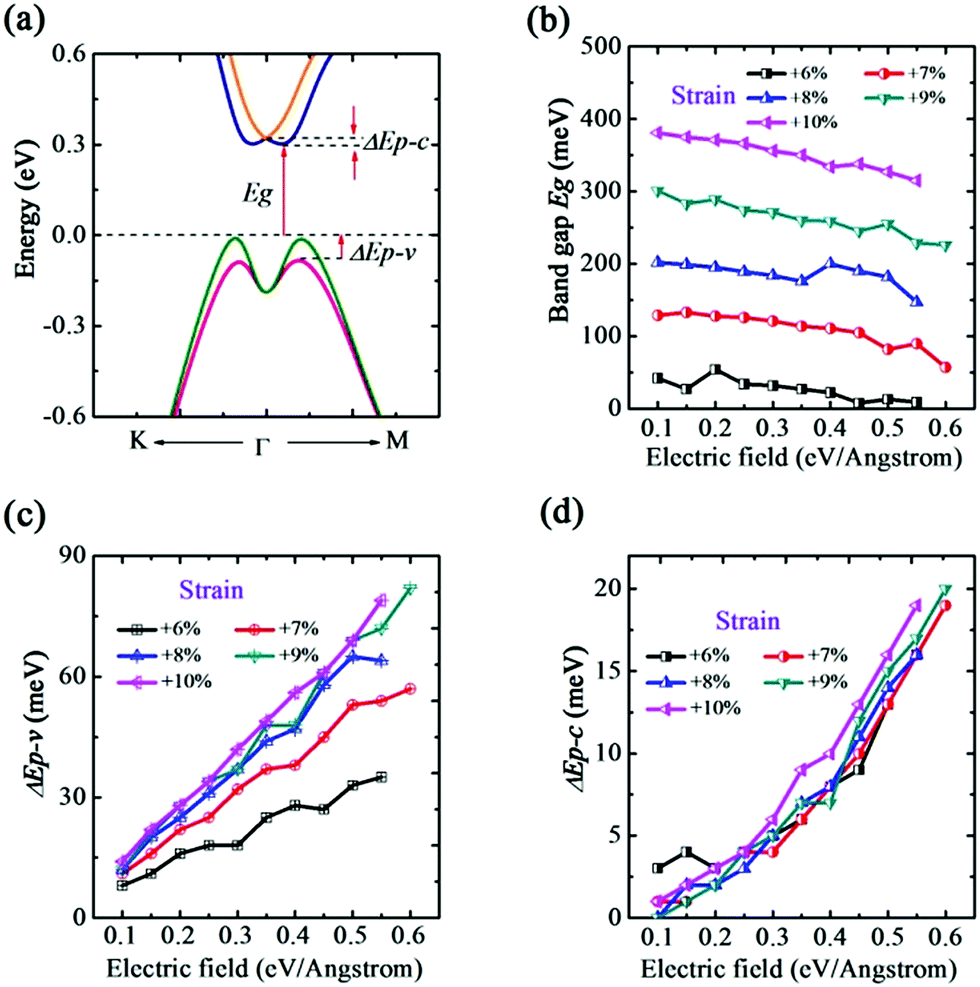 | ||
| Fig. 7 Using PBE + SOC method. (a) Electric field induced band splitting along K–Γ–M direction in strain range from +6% to +10%. (b) Electric field dependences of the band gap Eg. Electric field dependences of (c) the splitting energy of VBM ΔEp–v and (d) the splitting energy of CBM ΔEp–c with different strains. | ||
Now we begin to discuss the effect of both compressive strain and E-field applied at the same time. From the study of above mentioned it has known that a smaller compressive strain ε = −2% could transform the CBM from the Γ high symmetry point to the Γ–M direction. This change means that the CBM is very possible to be split by the external E-field. As predicted, the CBM has a band spin-splitting when ε is in the range of −2% to −7% (see Fig. 8(a)). It is noted that the splitting mechanism of the CBM in −2% to −7% is different from +6% to +10% owing to the different position of CBM in the Brillouin zone. Similar to above discussion, we also calculated the band gap Eg and splitting energy ΔEp–c and ΔEp–v. As seen in Fig. 8(b), Eg decreases monotonically with E-field. Under a same value of E-field, the larger is strain, the smaller is band gap. This situation is analogous to ε in −1% to +5%. However, we observe that, as seen in Fig. 8(c) and (d), both ΔEp–c and ΔEp–v increase with E-field even though ΔEp–c fluctuates at some ranges of E-field. Moreover, ΔEp–v is more sensitive to small compressive strain. Consequently, one can significantly tune the band splitting of VBM and CBM by the synergy effect. And we could expect that the strain and E-field tuned single b-bismuthene is applied to spintronic devices.
 | ||
| Fig. 8 Using PBE + SOC method. (a) Electric field induced band splitting along K–Γ–M direction in strain range from −2% to −7%. (b) Electric field dependences of the band gap Eg. Electric field dependences of (c) the splitting energy of VBM ΔEp–v and (d) the splitting energy of CBM ΔEp–c with different strains. | ||
In addition, we also probe into the E-field tuned bilayer b-bismuthene. Our results indicate that bilayer b-bismuthene undergoes the semimetal–metal character transition at Ec = 0.55 eV Å−1. As a result, the electronic phase transition induced by Ec of bilayer b-bismuthene is smaller than single one as a result of the existence of interlayer potential. Analogous to the single b-bismuthene, we find that E-field could also induce the band splitting in the VBM and CBM (see Fig. 9(a) and (b)) and ΔEp–c is larger than ΔEp–v, indicating a more sensitive splitting character in the CBM. When the value of E-field is changed to be negative, a similar conclusion is obtained. As seen Fig. 10(a)–(c), analysis of the band structure of three different interlayer distances evinces that the E-field induced band splitting depends on the interlayer distance in bilayer b-bismuthene. For instance, the VBM undergoes the splitting-degeneracy-splitting transition as the interlayer distance changes from 4.14 to 6.64 Å, since the VBM is located at the Γ high symmetry point when the interlayer distance is 5.94 Å. However, the CBM could always be split as the E-field applied, regardless of the interlayer distance. Therefore, it may be realized that we could control the band splitting of VBM by changing interlayer distance and exerting E-field. From Fig. 10(d), it suggests that E-field could effectively tune ΔEp–c and ΔEp–v except for ΔEp–v of d1 = 5.94 Å. It is worth mentioning that the interlayer distance retains nearly constant within the applied range of the external E-field.
 | ||
| Fig. 9 Using PBE + SOC method. (a) Electric field induced band splitting along K–Γ–M direction. (b) Electric field dependences of the splitting energy CBM ΔEp–c and VBM ΔEp–v of bilayer b-bismuthene. | ||
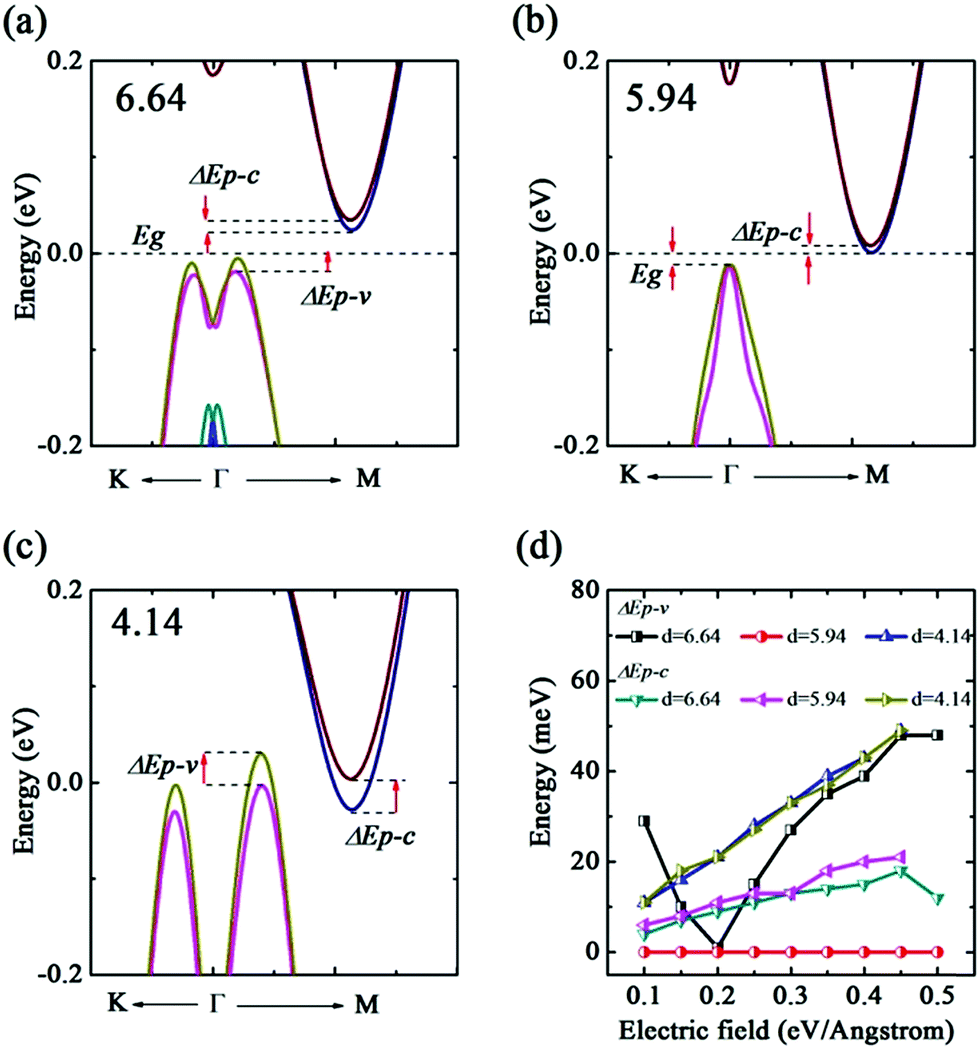 | ||
| Fig. 10 Using PBE + SOC method. Electric field induced band splitting along K–Γ–M direction of interlayer distance (a) 6.64, (b) 5.94, and (c) 4.14 Å. (d) Electric field dependences of the splitting energy of CBM ΔEp–c and VBM ΔEp–v with different interlayer distances. | ||
4 Conclusions
In summary, we systemically study the stability and electronic structure of strain and electric field tuned single and bilayer b-bismuthene. It has been suggested that single b-bismuthene is a stable semiconductor indirect band gap PBE + SOC method. There are indirect–direct and semiconducting–semimetallic transitions by stacking single b-bismuthene to bilayer b-bismuthene due to significant interlayer coupling. Similar transition in single b-bismuthene is also revealed by applying in-layer biaxial strain. Particularly, the Rashba energy can be effectively modulated by the in-layer biaxial strain. On the other hand, the band structure of bilayer b-bismuthene is found to be sensitive to the interlayer distance. Because of interlayer coupling altered, tuning interlayer distance can gain various electronic structures. Interestingly, the electric field can result in the band spin-degeneracy splitting near the VBM in single b-bismuthene, and the splitting energy increases with the strength of the electric field. More importantly, there is a synergy effect when both strain and electric field are applied at same time. The E-field induced band splitting character could be tuned by the strain strength. Our results demonstrate that the electronic structure of single and bilayer b-bismuthene is strain- and electric field-tunable, which provides valuable information for b-bismuthene as a promising candidate for the electronic and spintronic materials.Conflicts of interest
There are no conflicts to declare.Acknowledgements
This work was supported by National Natural Science Foundation of China (Grant No. 61366007 and No. 11164032 and No. 61066005), Program for New Century Excellent Talents in University (Grant No. NCET-12-1080), Applied Basic Research Foundation of Yunnan Province (Grant No. 2011CI003 and No. 2013FB007), Program of high-end scientific and technological talents in Yunnan Province (Grant No. 2013HA019), Program for Excellent Young Talents in Yunnan University. Computational resources were provided by the High Performance Computing Center of Yunnan University.References
- M. Xu, T. Liang, M. Shi and H. Chen, Chem. Rev., 2013, 113, 3766 CrossRef CAS PubMed.
- X. Song, J. Hu and H. Zeng, J. Mater. Chem. C, 2013, 1, 2952 RSC.
- K. S. Novoselov, A. K. Geim, S. V. Morozov, D. Jiang, M. I. Katsnelson, I. V. Grigorieva, S. V. Dubonos and A. A. Firsov, Nature, 2015, 438, 197 CrossRef PubMed.
- T. Akiyama, K. Nakamura and T. Ito, Jpn. J. Appl. Phys., 2016, 55, 04EP01 CrossRef.
- S. Cahangirov, M. Topsakal, E. Aktürk, H. Şahin and S. Ciraci, Phys. Rev. Lett., 2009, 102, 236804 CrossRef CAS PubMed.
- V. O. Özçelik, O. Ü. Aktürk, E. Durgun and S. Ciraci, Phys. Rev. B: Condens. Matter Mater. Phys., 2015, 92, 125420 CrossRef.
- J. Guan, Z. Zhu and D. Tománek, Phys. Rev. Lett., 2014, 113, 046804 CrossRef PubMed.
- Z. Zhu and D. Tománek, Phys. Rev. Lett., 2014, 112, 176802 CrossRef PubMed.
- C. Kamal and M. Ezawa, Phys. Rev. B: Condens. Matter Mater. Phys., 2015, 91, 085423 CrossRef.
- S. L. Zhang, Z. Yan, Y. F. Li, Z. F. Chen and H. B. Zeng, Angew. Chem., Int. Ed., 2015, 54, 3112 CrossRef CAS PubMed.
- Z. Zhu, J. Guan and D. Tománek, Phys. Rev. B: Condens. Matter Mater. Phys., 2015, 91, 161404(R) CrossRef.
- O. Ü. Aktürk, V. O. Özçelik and S. Ciraci, Phys. Rev. B: Condens. Matter Mater. Phys., 2015, 91, 235446 CrossRef.
- F. Ersan, E. Aktürk and S. Ciraci, Phys. Rev. B, 2016, 94, 245417 CrossRef.
- S. L. Zhang, M. Xie, F. Li, Z. Yan, Y. F. Li, E. Kan, W. Liu, Z. F. Chen and H. B. Zeng, Angew. Chem., Int. Ed. Engl., 2016, 128, 1698 CrossRef.
- M. Pumera and Z. Sofer, Adv. Mater., 2017, 1605299 CrossRef PubMed.
- A. Castellanos-Gomez, J. Phys. Chem. Lett., 2015, 6, 4280 CrossRef CAS PubMed.
- L. Kou, C. Chen and S. C. Smith, J. Phys. Chem. Lett., 2015, 6, 2794 CrossRef CAS PubMed.
- J. Qiao, X. Kong, Z. X. Hu, F. Yang and W. Ji, Nat. Commun., 2014, 5, 4475 CAS.
- V. Tran, R. Soklaski, Y. Liang and L. Yang, Phys. Rev. B: Condens. Matter Mater. Phys., 2014, 89, 235319 CrossRef.
- H. Liu, A. T. Neal, Z. Zhu, Z. Luo, X. Xu, D. Tomanek and P. D. Ye, ACS Nano, 2014, 8, 4033 CrossRef CAS PubMed.
- M. Elahi, K. Khaliji, S. M. Tabatabaei, M. Pourfath and R. Asgari, Phys. Rev. B: Condens. Matter Mater. Phys., 2015, 91, 115412 CrossRef.
- B. Ghosh, B. Singh, R. Prasad and A. Agarwal, Phys. Rev. B, 2016, 94, 205426 CrossRef.
- X. Peng, Q. Wei and A. Copple, Phys. Rev. B: Condens. Matter Mater. Phys., 2014, 90, 085402 CrossRef.
- L. Li, Y. Yu, G. J. Ye, Q. Ge, X. Ou, H. Wu, D. Feng, X. H. Chen and Y. Zhang, Nat. Nanotechnol., 2014, 9, 372 CrossRef CAS PubMed.
- P. Ares, F. Aguilar-Galindo, D. Rodriguez-San-Miguel, D. A. Aldave, S. Diaz-Tendero, M. Alcami, F. Martin, J. Gomez-Herrero and F. Zamora, Adv. Mater., 2016, 28, 6332 CrossRef CAS PubMed.
- E. Aktürk, O. Ü. Aktürk and S. Ciraci, Phys. Rev. B, 2016, 94, 014115 CrossRef.
- X. Gonze, J. P. Michenaud and J. P. Vigneron, Phys. Rev. B: Condens. Matter Mater. Phys., 1990, 41, 11827 CrossRef CAS.
- Y. M. Koroteev, G. Bihlmayer, E. V. Chulkov and S. Blügel, Phys. Rev. B: Condens. Matter Mater. Phys., 2008, 77, 045428 CrossRef.
- Y. M. Koroteev, G. Bihlmayer, J. E. Gayone, E. V. Chulkov, S. Blügel, P. M. Echenique and P. Hofmann, Phys. Rev. Lett., 2004, 93, 046403 CrossRef PubMed.
- P. Hofmann, Prog. Surf. Sci., 2006, 81, 191 CrossRef CAS.
- S. Murakami, Phys. Rev. Lett., 2006, 97, 236805 CrossRef PubMed.
- H. Mönig, J. Sun, Y. M. Koroteev, G. Bihlmayer, J. Wells, E. V. Chulkov, K. Pohl and P. Hofmann, Phys. Rev. B: Condens. Matter Mater. Phys., 2005, 72, 085410 CrossRef.
- Z. Liu, C. X. Liu, Y. S. Wu, W. H. Duan, F. Liu and J. Wu, Phys. Rev. Lett., 2011, 107, 136805 CrossRef PubMed.
- M. Wada, S. Murakami, F. Freimuth and G. Bihlmayer, Phys. Rev. B: Condens. Matter Mater. Phys., 2011, 83, 121310 CrossRef.
- L. Chen, Z. F. Wang and F. Liu, Phys. Rev. B: Condens. Matter Mater. Phys., 2013, 87, 235420 CrossRef.
- C. Niu, G. Bihlmayer, H. Zhang, D. Wortmann, S. Blügel and Y. Mokrousov, Phys. Rev. B: Condens. Matter Mater. Phys., 2015, 91, 041303(R) CrossRef.
- W. Yu, C. Y. Niu, Z. Zhu, X. Wang and W. B. Zhang, J. Mater. Chem. C, 2016, 4, 6581 RSC.
- M. Y. Liu, Y. Huang, Q. Y. Chen, C. Cao and Y. He, Sci. Rep., 2016, 6, 29114 CrossRef CAS PubMed.
- S. Zhang, M. Xie, B. Cai, H. Zhang, Y. Ma, Z. Chen, Z. Zhu, Z. Hu and H. Zeng, Phys. Rev. B: Condens. Matter Mater. Phys., 2016, 93, 245303 CrossRef.
- T. Hirahara, N. Fukui, T. Shirasawa, M. Yamada, M. Aitani, H. Miyazaki, M. Matsunami, S. Kimura, S. Takahashi, S. Hasegawa and K. Kobayashi, Phys. Rev. Lett., 2012, 109, 227401 CrossRef CAS PubMed.
- Z. F. Wang, M. Y. Yao, W. Ming, L. Miao, F. Zhu, C. Liu, C. L. Gao, D. Qian, J. F. Jia and F. Liu, Nat. Commun., 2013, 4, 1384 CrossRef CAS PubMed.
- G. Kresse and J. Furthmuller, Phys. Rev. B: Condens. Matter Mater. Phys., 1996, 54, 11169 CrossRef CAS.
- J. P. Perdew, K. Burke and M. Ernzerhof, Phys. Rev. Lett., 1996, 77, 3865 CrossRef CAS PubMed.
- J. Heyd, G. E. Scuseria and M. Ernzerhof, J. Chem. Phys., 2003, 118, 8207 CrossRef CAS.
- S. Grimme, J. Antony, S. Ehrlich and H. Krieg, J. Chem. Phys., 2010, 132, 154104 CrossRef PubMed.
- R. G. Pearson, Proc. Natl. Acad. Sci. U. S. A., 1975, 72, 2104 CrossRef CAS.
- L. Cheng, H. Liu, X. Tan, J. Zhang, J. Wei, H. Lv, J. Shi and X. Tang, J. Phys. Chem. C, 2014, 118, 904 CAS.
- J. Lee, W. C. Tian, W. L. Wang and D. X. Yao, Sci. Rep., 2015, 5, 11512 CrossRef PubMed.
- R. Zacharia, H. Ulbricht and T. Hertel, Phys. Rev. B: Condens. Matter Mater. Phys., 2004, 69, 155406 CrossRef.
- M. S. Bahramy, R. Arita and N. Nagaosa, Phys. Rev. B: Condens. Matter Mater. Phys., 2011, 84, 041202(R) CrossRef.
- L. Kou, X. Tan, Y. Ma, H. Tahini, L. Zhou, Z. Sun, D. Aijun, C. Chen and S. C. Smith, 2D Mater., 2015, 2, 045010 CrossRef.
- L. Shulenburger, A. D. Baczewski, Z. Zhu, J. Guan and D. Tomanek, Nano Lett., 2015, 15, 8170 CrossRef CAS PubMed.
- R. Q. Zhang, C. Hou, N. Gao, Z. Wen and Q. Jiang, ChemPhysChem, 2011, 12, 1302 CrossRef CAS PubMed.
Footnote |
| † Electronic supplementary information (ESI) available. See DOI: 10.1039/c7ra05787c |
| This journal is © The Royal Society of Chemistry 2017 |