
 Open Access Article
 This Open Access Article is licensed under a
 Creative Commons Attribution 3.0 Unported Licence
A facile approach for photoelectrochemical performance enhancement of CdS QD-sensitized TiO2 via decorating {001} facet-exposed nano-polyhedrons onto nanotubes†
Dong Ding,
Bo Zhou,
Shurong Liu,
Guijie Zhu,
Xianwei Meng,
Jiandong Yang,
Wuyou Fu and
Haibin Yang*
and
Haibin Yang*
State Key Laboratory of Superhard Materials, Jilin University, Changchun 130012, P. R. China. E-mail: yanghb@jlu.edu.cn; Tel: +86 431 85168763
First published on 25th July 2017
Abstract
In this study, we report a TiO2 hybrid structure prepared by a facile route, wherein TiF62− ion has been used as both the surfactant and titanium source. Single-crystalline TiO2 nano-polyhedrons with exposed high active {001} facets were grown on a TiO2 nanowire and nanotube (TWTs) films. This hybrid structure served as a model architecture for efficient photoelectrochemical (PEC) devices because it simultaneously offered a large contact area with the electrolyte and direct pathway for photoexcited electron collection. Under simulated sunlight illumination (AM 1.5 light at 100 mW cm−2), this hybrid structure exhibited a photocurrent density of 1.36 mA cm−2 at 0 V vs. Ag/AgCl (JSC) and photoconversion efficiency (η) of 0.81% at −0.51 V vs. Ag/AgCl, nearly 2.4 times higher than those of the bare TWTs. Morphology of the TiO2 nano-polyhedrons in the hybrid structure was greatly influenced by the TiF62− ion concentration, and a proper concentration was determined to be 2.5 mM. Moreover, the CdS QDs were sensitized onto the hybrid structure, and their JSC and η reached 2.31 mA cm−2 & 1.94%, respectively, 1.5 times higher than those of the CdS-sensitized bare TWTs. The TiO2 nano-polyhedrons improved the efficiency via increasing the specific surface area of the electrode, thus facilitating hole transfer into the electrolyte. Moreover, the exposed high reactive {001} facets provided more effective area for the adsorption of CdS, leading to an enhanced photogeneration carrier density.
1. Introduction
Anatase TiO2 has been vastly explored in solar energy conversion owing to its advantages of favorable photooxidation power, easy availability, good chemical stability, and nontoxicity,1,2 which has outstanding performances as photoelectrodes in photoelectrochemical (PEC) fields such as in photocatalysis, photovoltaics, and water splitting.3–7 PEC performance is mainly determined by the amount of photo-generated electron–hole pairs, which are driven by large specific surface area and high photoactivity of the TiO2 photoanode according to the Honda–Fujishima effect.8–10 The TiO2 hybrid structure, which can combine the advantages of different morphologies and effectively enlarge specific surface area, is an ongoing hot research topic.11–16 Y. Tang et al. have grown TiO2 nanoparticles on TiO2 nanoflakes; the obtained hierarchical porous hybrid structure has a larger specific surface area than the TiO2 nanosheets and nanoparticles and higher photocatalytic activity for the degradation of organic compounds.17 Dongsheng Xu et al. have prepared hetero-structured TiO2 nanotree arrays with rutile trunks and anatase branches. The hybrid structure can deposit more CdS/CdSe QDs and improve the conversion efficiency of the whole device.18 Compared with TiO2 nanostructures in other forms, highly ordered TiO2 nanotubes and nanowires (TWTs) are anticipated to possess unidirectional electrical channels and high specific surface area, which show promising properties due to their slower recombination and higher charge collection efficiency. Therefore, a structural modification strategy for preparing a hybrid structure based on TWTs is highly desirable.Moreover, PEC performance of TiO2 is closely associated with its exposed facets; theoretical and experimental studies reveal that the {001} facets achieve higher chemical activities than {101} and {100} facets in the anatase TiO2 crystals (the average surface energies of anatase TiO2 are in the order γ {001} (0.90 J m−2) > γ {100} (0.53 J m−2) > γ {101} (0.44 J m−2)).19 This can be attributed to the larger Ti–O–Ti bond angle on the {001} facets, which make the 2p states of the surface O atoms unstable and very reactive.20 However, according to the Wulff construction, the {001} facets tend to diminish during the free crystal growth process to minimize the total surface energy.21,22 Surfactant-assisted method is a popular approach for the controlled synthesis of {001} facet-exposed anatase TiO2, in which F− are introduced as surfactants.23,24 Lu et al. used TiF4 and HF as raw materials in a Teflon-lined autoclave to prepare {001} facet-exposed TiO2 single crystals and found that the {001} facets played crucial roles in photoreactivity improvement of TiO2.25,26 Pan et al. have prepared N + Ni co-doped anatase TiO2 nanocrystals with exposed {001} facets using a two-step hydrothermal reaction, and the as-prepared sample showed a superior photocatalytic activity.27 The synthesized TiO2 single crystals and TWT hybrid structure with highly reactive {001} facets can have potential applications in several areas such as in photocatalytic CO2 reduction, solar cells, and photonic and optoelectronic devices.
In this study, we synthesized a novel TiO2 hybrid structure via a facile route, as illustrated in Scheme 1. First, highly ordered TiO2 nanotubes and nanowires (TWTs) on a Ti foil were prepared by electrochemical anodization. Second, single-crystalline TiO2 nano-polyhedrons with exposed {001} facets were grown on TWTs through a chemical bath deposition (CBD) process under atmospheric pressure, wherein TiF62− was used as both the surfactant and titanium source. We conducted varied TiF62− concentration studies during the CBD process and proposed a possible growth mechanism. Third, CdS QDs were assembled onto bare TWTs and hybrid structure via successive ionic layer adsorption and reaction (SILAR) technique. CdS (Eg ≈ 2.4 eV) sensitization is considered as an effective method to broaden the solar absorption spectrum of TiO2 (Eg ≈ 3.2 eV). Thus, we obtained a hybrid structure with superior PEC performance than bare TWTs owing to its preponderances of increased surface area and exposed highly reactive {001} facets.
 | ||
| Scheme 1 Schematic of the preparation process. | ||
2. Experimental
2.1 Preparation of the hybrid structure
Bare TWTs were prepared via electrochemical anodization of a Ti foil (99.9% purity) using a direct current (dc) stabilized voltage and current power supply (WYJ60V3A, Pingguo Instrumentation Co. Ltd. China) at a constant voltage of 40 V for 1 h. The Ti foil and a graphite plate were used as the anode and cathode, respectively. Electrolyte solution contained 0.3 wt% NH4F, 95.0 vol% ethylene glycol, and 5.0 vol% deionized H2O. The as-prepared photoelectrode was thoroughly washed with ethanol and DI water and then annealed in air at 450 °C for 2 h. TiO2 nano-polyhedrons were grown on TWTs via chemical bath deposition, i.e., TWTs were immersed in an aqueous solution containing 2.5 mM (NH4)2TiF6 at 80 °C for 30 min; then, the sample was washed with DI water and annealed in air at 450 °C for 1 h.2.2 Preparation of the CdS-sensitized hybrid structure
In detail, the sample was successively immersed in 0.5 M mercaptoacetic acid (TGA) and then in 0.5 M Cd(NO3)2·4H2O in ethanol and finally in 0.5 M Na2S in deionized water. Each immersion was performed for 10 min; the photoelectrode was then rinsed successively with pure ethanol and deionized water to remove excess precursors and dried in air before the next dipping cycle. This abovementioned process was repeated six times. CdS-sensitized bare TWTs were prepared under the same conditions for comparison.2.3 Sample characterization
Scanning electron microscopy (SEM) images were obtained using a field-emission SEM (JEOL JSM-6700F). Transmission electron microscopy (TEM) and high-resolution TEM (HRTEM) images and EDS mapping were obtained using a JEM-2100F high-resolution transmission microscope operating at 200 kV. Optical characterization (UV-vis absorption spectra) of the film was performed using a UV-3150 double-beam spectro-photometer (Shimadzu UV-3150). X-ray diffraction (XRD) spectra of the samples were obtained using a Rigaku D/max-2500 X-ray diffractometer with Cu Kα radiation (λ = 1.5418 Å).PEC performance of the samples was analysed via an electrochemical workstation (CH Instruments, model CHI601C) using a Ag/AgCl reference electrode and a Pt wire as the counter electrode. A 500 W Xe lamp (Spectra Physics) with a monochromator simulated sunlight, which was adjusted to provide AM 1.5 light at 100 mW cm−2 using a laser power meter (BG26M92C, Midwest Group). The electrolyte solution consisted of 0.25 M Na2S·9H2O, 0.35 M Na2SO3, and 0.1 M KCl aqueous solution (pH = 12). The photoconversion efficiency (η) was calculated from the line sweep voltammogram as follows:28,29
| η = JSC(Eo − E)/I |
The IPCE of the samples were measured using a two-electrode system with an action spectrum measurement setup (PEC-S20, Peccell Ltd.). Before the measurement, the samples were sealed in sandwich structures with a 60 μm spacer using Pt as the counter electrode. The electrolyte was injected between the two electrodes. Light was irradiated from the counter electrode side.
3. Results and discussion
For obtaining TiO2 hybrid structures, 2.5 mM TiF62− bath was taken out for 30 minutes as an additional treatment after the traditional anodizing process. Fig. 1A and B show the top-view and side-view SEM images of the as-prepared sample, respectively. Herein, three major morphologies, i.e. nanotubes, nanowires, and nano-polyhedrons, can be observed. Nanotubes with a split top are highly orderly arranged and exhibit an average length of ∼3 μm and diameter of ∼73.3 nm (Fig. S1 in ESI†). Nano-polyhedrons (truncated octahedrons) are grown on both side and split top sites of the TWTs with an average size of ∼91.5 nm, and the relative TEM images are shown in the ESI (Fig. S2†). Fig. 1C shows the HRTEM and fast Fourier transform (FFT) images of the selected area of nano-polyhedrons. Interplanar spacings of 0.352 nm and 0.475 nm with an interfacial angle of 68.3° are consistent with those of the (101) and (002) facets of anatase TiO2 (JCPDS no. 71-1167), respectively. FFT patterns in the inset refer to the (101) and (002) facets. Furthermore, a (101) zone-axis could be deduced, where the exposed surfaces were bound by the {101} and {001} facets. Fig. 1D shows the interface of the nanowire and nano-polyhedron. A clear boundary further confirms that single-crystalline nano-polyhedrons are bonded on nanowires. The crystal structure of the hybrid structure is examined by X-ray diffraction (XRD), as shown in Fig. 1E. The diffraction peaks are indexed to the anatase-phase TiO2 (JCPDS no. 71-1167) and Ti, further demonstrating that the as-synthesized hybrid structure grown on Ti is pure anatase TiO2.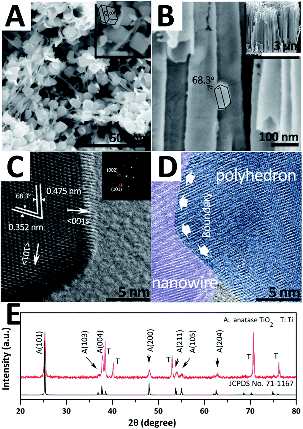 | ||
| Fig. 1 SEM images (A and B), HRTEM and FFT images (C and D), and XRD pattern (E) of hybrid structure. | ||
In a typical anodizing system, Ti is corroded into TiF62− by F− under electric current; thereafter, TiF62− hydrolyses into Ti(OH)4, and the stacking blocks of the nanotube. Then, the nanotubes undergo an annealing process in which Ti–O–Ti are joined via dehydration. When the sample is merged into the TiF62− solution, TiO2 nucleates on nanotubes and grows into nano-polyhedrons. Fig. 2 and S3† show the SEM images of the samples synthesized at the TiF62− concentration of 0.5 mM, 1.5 mM, 2.5 mM, and 3.5 mM (denoted as S-0.5/1.5/2.5/3.5, respectively). As TiF62− concentration increases from 0.5 mM to 2.5 mM, the grain size of the polyhedron increases from 22.5 nm to 91.5 nm and the shape becomes regular. We deduced that the TiO2 nano-polyhedrons were formed through the hydrolysis of TiF62− through the following reaction:
| [TiF6]2− + nH2O ↔ [Ti(OH)nF6−n]2− + nHF |
| [Ti(OH)6]2− + 2H+ → TiO2 + 4H2O |
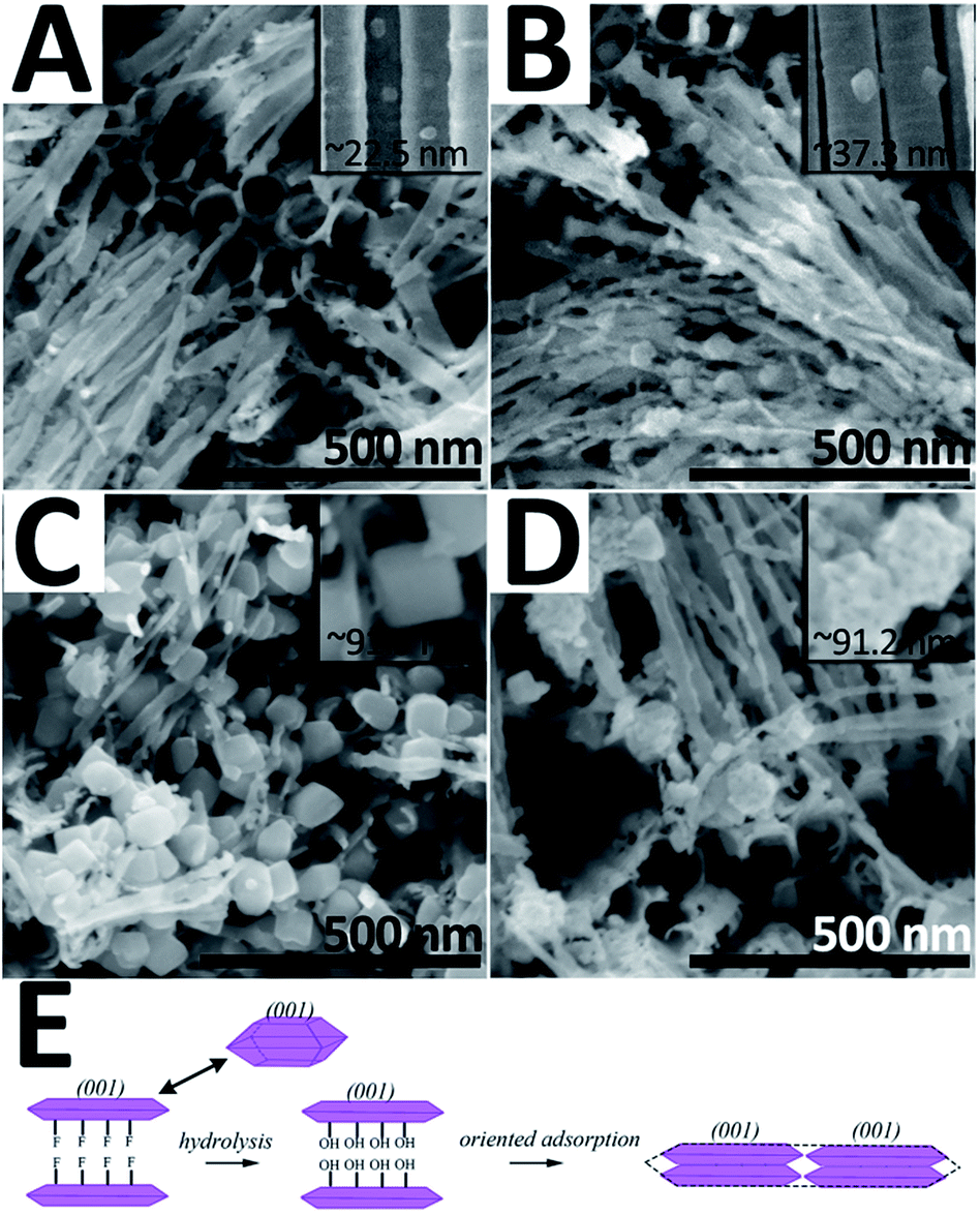 | ||
| Fig. 2 SEM images of the hybrid structure synthesized at varied TiF62− concentrations: 0.5 mM (A), 1.5 mM (B), 2.5 mM (C), and 3.5 mM (D). Schematic showing the TiO2 nano-polyhedron formation (E). | ||
Usually, TiO62− octahedra are the building blocks of TiO2. As illustrated in Fig. 2E, F− generated by hydrolysis process could favorably adsorb on the high active {001} facets of TiO2 and suppress the growth along the [001] direction. Consequently, the resulting TiO2 crystal nucleus maintains the {001} facet-exposed truncated octahedral structure.25 When the TWTs are immersed in TiF62− solution, TiO2 nucleates on TWTs and grows into nano-polyhedrons. When the TiF62− concentration increases, the surface of these {001} facets-exposed TiO2 crystal nucleus hydrolyzes and F− would be replaced by hydroxyl groups; then, the oriented adsorption process occurs under the influence of dehydration condensation reaction between hydroxyl groups. Hence, the size of the TiO2 nano-polyhedrons becomes larger. This indicates that at this stage, the TiF62− concentration is the main parameter affecting the growth of the polyhedrons; as the TiF62− concentration increases, the system can afford enough growth dynamic to gradually form an entire (001) low-energy surface. However, when the TiF62− concentration further increases to 3.5 mM, the grain size remains ∼91 nm, but the surfaces become rough. This can be attributed to further nucleation on the polyhedron surfaces caused by extreme undercooling.
PEC performance of the hybrid structure samples prepared at different TiF62− concentrations is shown in Fig. S6.† The S-2.5 sample shows the best PEC performance owing to the greater specific surface area and exposed {001} facets. On the other hand, when the TiF62− concentration reaches 3.5 mM, randomly deposited TiO2 crystal nuclei on the nano-polyhedrons cover the high active {001} facets and result in a decreased JSC and η. In this study, the S-2.5 sample has been chosen for the following CdS QD sensitization investigation. The CdS QD-sensitized bare TWTs were prepared and investigated for comparison.
The as-prepared hybrid structure samples were further sensitized by CdS QDs, as shown in Fig. 3. Fig. 3A and B show the top- and side-view SEM images. The surfaces of the arrayed TWTs and nano-polyhedrons are decorated by evenly distributed CdS QDs and become rough. Moreover, the CdS QDs on the TWTs and nano-polyhedrons are investigated by HRTEM, as shown in Fig. 3C and D, respectively. The average size of the CdS QDs is ∼5.3 nm. The d-spacings of the clear crystalline structure are 0.335 nm, 0.205 nm, and 0.352 nm, that can be indexed to (111) and (220) of CdS (JCPDS no. 80-0019) and (101) of anatase TiO2, respectively. EDS mapping of the sample is shown in Fig. 3E and the corresponding line scan profile of EDX spectra is shown in the ESI (Fig. S9†). The distribution and counts of the Cd and S elements are very similar, but different from those of the Ti and O elements; this indicates that the CdS crystal is the only form in which Cd and S exist. Fig. 3F shows the UV-vis spectra of the original sample and the sensitized sample. The absorption range greatly enlarges from ∼380 nm to 570 nm. The tuned band gap indicates that CdS QDs are well bonded onto the TiO2 hybrid structure and provide a good electronic transmission channel. Fig. 3G shows the XRD patterns of the sample. A new peak at 2θ = 26.5° is observed and indexed to CdS, which is in accordance with the abovementioned HRTEM results.
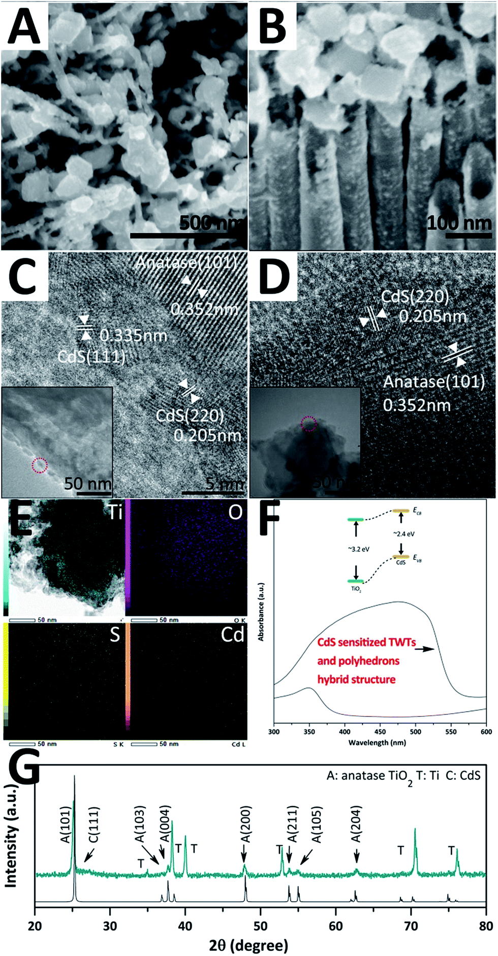 | ||
| Fig. 3 SEM images (A and B), TEM and HRTEM images (C and D), EDS mapping (E), UV-vis spectra (F), and XRD patterns (G) of the CdS-sensitized hybrid structure. | ||
Photocurrent is usually seen as one of the key parameters of PEC performance and reflects the transfer efficiency of photo-excited electrons. Fig. 4A presents the photocurrent density characteristics (J–V curves) and photoconversion efficiencies of the samples. The photocurrent density at 0 V vs. Ag/AgCl (JSC) and photoconversion efficiency (η) of the hybrid structure are 1.36 mA cm−2 and 0.81% (−0.51 V vs. Ag/AgCl), respectively, nearly 2.4 times higher than those of bare TWTs (0.57 mA cm−2 and 0.35% at −0.42 V vs. Ag/AgCl). Furthermore, JSC and η of 1.53 mA cm−2 and 1.14% (−0.69 V vs. Ag/AgCl), respectively, were attained for the CdS-sensitized TWTs. These results confirm that CdS QD sensitization is an effective method for enhancing the PEC performance of TWTs. The JSC and η of the CdS-sensitized hybrid structure are found to be 2.31 mA cm−2 and 1.94% (−0.65 V vs. Ag/AgCl), respectively, about 1.5 times those of the CdS-sensitized bare TWTs, and the hybrid structure can boost the JSC and η of bare TWTs by up to 400%. Moreover, the PEC performance of the electrodes at various wavelengths was measured by the IPCE test. As shown in Fig. 4B, the best IPCE of the CdS-sensitized hybrid structure electrode is around 25% across the absorption ranges, which is higher than those of other electrodes (14% for CdS-sensitized TWTs > 6% for hybrid structure > 2% for TWTs), indicating that electron–hole pairs are more efficiently separated in the CdS-sensitized hybrid structure electrode. IPCE results of the samples are in accordance with the corresponding absorption spectra as well as the corresponding photocurrent–voltage (J–V) curves. Stability, reproducibility, and repeatability of the samples can be represented by transient photocurrent (J–T) plots. We generated the J–T plots at 0 V vs. Ag/AgCl under chopped illumination. The J–T responses of the samples are shown in Fig. 4C; all the samples show relatively good reproducibility and stability when illumination is turned on and off. The observed dark current densities (light off) for all the samples are negligible. It is obvious that the effect of CdS is more prominent in the CdS-sensitized hybrid structure system as a result of the improved distribution of the CdS QDs and the effective separation of the photo-generated charges.
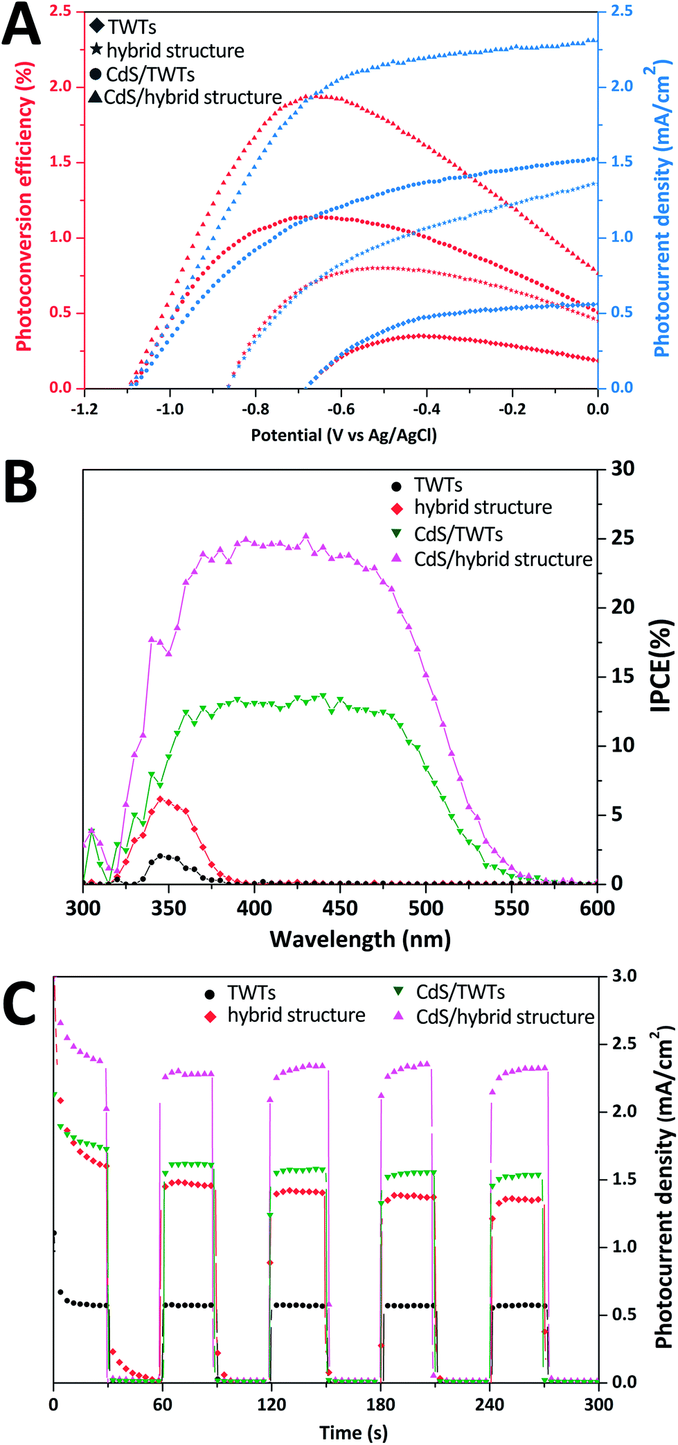 | ||
| Fig. 4 J–V curves and photoconversion efficiencies (A), IPCE data (B), and J–T curves under chopped illumination (C) of TWTs, hybrid structure, CdS-sensitized TWTs, and CdS-sensitized hybrid structure. | ||
The superior PEC performance of the CdS-sensitized hybrid structure can be ascribed to the following reasons: as illustrated in Fig. 5, the TiO2 nano-polyhedrons grown on TWTs not only increase the specific surface area of the electrode but also improve light utilization owing to the exposed highly active {001} facets. It is also noteworthy that a higher specific surface area can increase the interface are as between the electrode and electrolyte, which can effectively reduce the recombination rate of photo-generated electron–hole pairs and thus enhance the photocurrent density. Moreover, the TiO2 nano-polyhedrons grown on TWTs with highly active {001} facets provide more effective area for the adsorption of CdS, thus increasing the generation of electron–hole pairs. Moreover, as the conduction band edge of CdS is higher than that of TiO2, a type-II band structure is formed between CdS and TiO2, facilitating the transfer of photo-generated electrons from CdS to TiO2. The photoexcited electrons then move from CdS to TiO2 nano-polyhedrons or move from CdS to TWTs and are gathered on the Ti substrate; this leads to a considerably reduced electron–hole recombination and enhanced photocurrent and efficiency.
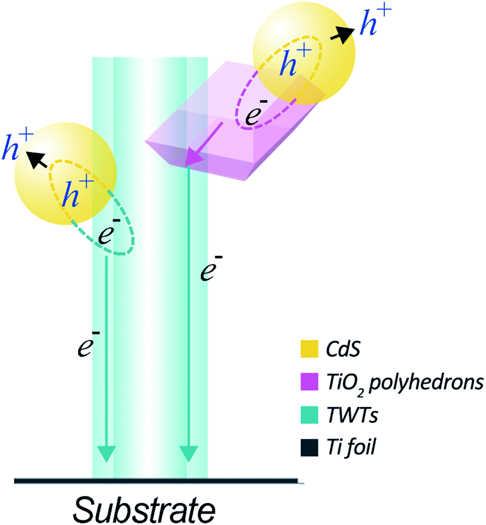 | ||
| Fig. 5 Schematic showing the charge-transfer processes between CdS QDs and hybrid structure. | ||
4. Conclusions
In summary, the TiO2 hybrid structure with highly active {001} facets was fabricated via a facile method, which exhibited higher specific surface area and enhanced PEC performance. Under simulated sunlight illumination (AM 1.5 light at 100 mW cm−2), JSC and η of the hybrid structure were 1.36 mA cm−2 and 0.81%, respectively, nearly 2.4 times higher than those of TWTs. Moreover, the CdS-sensitized hybrid structure showed a superior PEC performance over the CdS-sensitized bare TWTs owing to the larger specific surface area and enhanced activity provided by nano-polyhedrons grown on the TWTs. JSC and η of the CdS-sensitized hybrid structure were 2.31 mA cm−2 & 1.94%, respectively, about 1.5 times those of the CdS-sensitized TWTs, and the hybrid structure can boost the JSC and η values of bare TWTs by up to 400%. Thus, this TiO2 hybrid structure can be an ideal candidate to construct a photoanode for water splitting and photocatalysis.Conflicts of interest
There are no conflicts of interest to declare.Acknowledgements
This work was supported by the Technology Development Program of Jilin Province (Grant no. 20130206078GX).References
- X. Chen and S. S. Mao, Titanium Dioxide Nanomaterials: Synthesis, Properties, Modifications, and Applications, Chem. Rev., 2007, 107, 2891–2959 CrossRef CAS PubMed.
- J. Zhang, Y. Zhang, Y. Lei and C. Pan, Photocatalytic and Degradation Mechanisms of Anatase TiO2: A HRTEM Study, Catal. Sci. Technol., 2011, 1, 273–278 CAS.
- L. Kavan, M. Grätzel, S. E. Gilbert, C. Klemenz and H. J. Scheel, Electrochemical and photoelectrochemical investigation of single-crystal anatase, J. Am. Chem. Soc., 1996, 118, 6716–6723 CrossRef CAS.
- G. S. Li, L. Wu, F. Li, P. Xu, D. Q. Zhang and H. X. Li, Photoelectrocatalytic Degradation of Organic Pollutants Via a CdS Quantum Dots Enhanced TiO2 Nanotube Array Electrode under Visible Light Irradiation, Nanoscale, 2013, 5, 2118–2125 RSC.
- M. Liu, J. Zheng, Q. Liu, S. Xu, M. Wu, Q. Xue, Z. Yan, H. Xiao, Z. Wei and H. Zhu, The Preparation, Load and Photocatalytic Performance of N-Doped and CdS-Coupled TiO2, RSC Adv., 2013, 3, 9483–9489 RSC.
- I. Mora-Seró, S. Giménez, F. Fabregat-Santiago, R. Gómez, Q. Shen, T. Toyoda and J. Bisquert, Recombination in Quantum Dot Sensitized Solar Cells, Acc. Chem. Res., 2009, 42, 1848–1857 CrossRef PubMed.
- Y. Li, X. Wei and B. Zhu, et al., Hierarchically branched Fe2O3@TiO2 nanorod arrays for photoelectrochemical water splitting: facile synthesis and enhanced photoelectrochemical performance, Nanoscale, 2016, 8, 11284–11290 RSC.
- A. Fujishima and K. Honda, Electrochemical photolysis of water at a semiconductor electrode, Nature, 1972, 238, 37 CrossRef CAS PubMed.
- M. Xu, P. Da, H. Wu, D. Zhao and G. Zheng, Controlled Sn-Doping in TiO2 Nanowire Photoanodes with Enhanced Photoelectrochemical Conversion, Nano Lett., 2012, 12, 1503–1508 CrossRef CAS PubMed.
- P. D. Yang, D. Y. Zhao and D. I. Margolese, et al., Block Copolymer Templating Syntheses of Mesoporous Metal Oxides with Large Ordering Lengths and Semicrystalline Framework, Chem. Mater., 2017, 11, 2813–2826 CrossRef.
- Y. C. Wang, Y. Zhang, J. Tang, H. Y. Wu, M. Xu, Z. Peng, X. G. Gong and G. F. Zheng, Simultaneous Etching and Doping of TiO2 Nanowire Arrays for Enhanced Photoelectrochemical Performance, ACS Nano, 2013, 7, 9375–9383 CrossRef CAS PubMed.
- N. K. Allam, F. Alamgir and M. A. El-Sayed, Enhanced Photoassisted Water Electrolysis Using Vertically Oriented Anodically Fabricated Ti-Nb-Zr-O Mixed Oxide Nanotube Arrays, ACS Nano, 2010, 4, 5819–5826 CrossRef CAS PubMed.
- B. Sun, et al., Decoration of TiO2 Nanotube Arrays By Graphitic-C3N4 Quantum Dots with Improved Photoelectrocatalytic Performance, Appl. Surf. Sci., 2017, 394, 479–487 CrossRef CAS.
- K. Naito, T. Tachikawa, M. Fujitsuka and T. Majima, Single-molecule observation of photocatalytic reaction in TiO2 nanotube: importance of molecular transport through porous structures, J. Am. Chem. Soc., 2009, 131, 934–936 CrossRef CAS PubMed.
- J. H. Ping, et al., High-Performance Large-Scale Flexible Dye-Sensitized Solar Cells Based on Anodic TiO2 Nanotube Arrays, ACS Appl. Mater. Interfaces, 2013, 20, 10098–10104 Search PubMed.
- G. Liu, X. Liu and L. Wang, et al., Hierarchical Li4Ti5O12-TiO2, microspheres assembled from nanoflakes with exposed Li4Ti5O12-TiO2, (011) and anatase TiO2, (001) facets for high-performance lithium-ion batteries, Electrochim. Acta, 2016, 222, 1103–1111 CrossRef CAS.
- Y. Tang, P. Wee and Y. Lai, et al., Hierarchical TiO2 Nanoflakes and Nanoparticles Hybrid Structure for Improved Photocatalytic Activity, J. Phys. Chem. C, 2015, 116, 2772–2780 Search PubMed.
- F. Zhu, H. Dong, Y. Wang, D. P. Wu, J. M. Li, J. L. Pan, Q. Li, X. C. Ai, J. P. Zhang and D. S. Xu, Dual-functional hetero-structured TiO2 nanotrees composed of rutile trunks and anatase branches for improved performance of quantum dot-sensitized solar cells, Phys. Chem. Chem. Phys., 2013, 15, 17798–17803 RSC.
- M. Lazzeri, A. Vittadini and A. Selloni, Structure and Energetics of Stoichiometric TiO2 Anatase Surfaces, Phys. Rev. B, 2002, 65, 119901 CrossRef.
- J. G. Yu, J. X. Low, W. Xiao, P. Zhou and M. Jaroniec, Enhanced Photocatalytic CO2-Reduction Activity of Anatase TiO2 by Coexposed {001} and {101} Facets, J. Am. Chem. Soc., 2014, 136, 8839–8842 CrossRef CAS PubMed.
- X. Han, Q. Kuang, M. Jin, Z. Xie and L. Zheng, Synthesis of titania nanosheets with a high percentage of exposed (001) facets and related photocatalytic properties, J. Am. Chem. Soc., 2009, 131, 3152–3153 CrossRef CAS PubMed.
- A. Selloni, Crystal growth: anatase shows its reactive side, Nat. Mater., 2008, 7, 613–615 CrossRef CAS PubMed.
- C. Chen, R. Hu, K. G. Mai, Z. M. Ren, H. Wang, G. D. Qian and Z. Y. Wang, Shape Evolution of Highly Crystalline Anatase TiO2 Nanobipyramids, Cryst. Growth Des., 2011, 11, 5221–5226 CAS.
- G. Liu, H. G. Yang, X. Wang, L. Cheng, J. Pan, G. Q. Lu and H. M. Cheng, Visible light responsive nitrogen doped anatase TiO2 sheets with dominant {001} facets derived from TiN, J. Am. Chem. Soc., 2009, 131, 12868–12869 CrossRef CAS PubMed.
- H. G. Yang, C. H. Sun, S. Z. Qiao, J. Zou, G. Liu, S. C. Smith, H. M. Chen and G. Q. Lu, Anatase TiO2 Single Crystals with a Large Percentage of Reactive Facets, Nature, 2008, 453, 638–641 CrossRef CAS PubMed.
- H. G. Yang, G. Liu, S. Z. Qiao, C. H. Sun, Y. G. Jin, S. C. Smith, J. Zou, H. M. Chen and G. Q. Lu, Solvothermal Synthesis and Photoreactivity of Anatase TiO2 Nanosheets with Dominant {001} Facets, J. Am. Chem. Soc., 2009, 131, 4078–4083 CrossRef CAS PubMed.
- Y. P. Zhang, C. Z. Li and C. X. Pan, N + Ni Codoped Anatase TiO2 Nanocrystals with Exposed {001} Facets Through Two-Step Hydrothermal Route, J. Am. Ceram. Soc., 2012, 95, 2951–2956 CrossRef CAS.
- S. U. M. Khan, M. Al-Shahry and W. B. Ingler Jr, Efficient Photochemical Water Splitting by a Chemically Modified n-TiO2, Science, 2002, 297, 2243–2245 CrossRef CAS PubMed.
- W. J. Sheng, B. Sun, T. L. Shi, X. H. Tan, Z. C. Peng and G. L. Liao, Quantum Dot-Sensitized Hierarchical Micro/Nanowire Architecture for Photoelectrochemical Water Splitting, ACS Nano, 2014, 8, 7163–7169 CrossRef CAS PubMed.
Footnote |
| † Electronic supplementary information (ESI) available: Fig. S1 TEM images of hybrid structure. Fig. S2 XPS spectrum of hybrid structure. Fig. S3 PEC performance of hybrid structure samples prepared under different TiF62− concentration: J–V curves (A), photoconversion efficiencies (B). Fig. S4 SEM images of bare TWTs (A and B), CdS sensitized bare TWTs (C and D). Fig. S5 line scan profile of EDX spectra of CdS sensitized hybrid structure. See DOI: 10.1039/c7ra05772e |
| This journal is © The Royal Society of Chemistry 2017 |