
 Open Access Article
 This Open Access Article is licensed under a Creative Commons Attribution-Non Commercial 3.0 Unported Licence
L-Cysteine assisted-synthesis of 3D In2S3 for 3D CuInS2 and its application in hybrid solar cells
Wenjin Yue *a,
Feiyu Weia,
Chenbin Hea,
Dandan Wua,
Nengwen Tanga and
Qiquan Qiao*b
*a,
Feiyu Weia,
Chenbin Hea,
Dandan Wua,
Nengwen Tanga and
Qiquan Qiao*b
aSchool of Biochemical Engineering, Anhui Polytechnic University, Wuhu, 241000, P. R. China. E-mail: yuewenjin_79@163.com
bCentre for Advanced Photovoltaics, Department of Electrical Engineering and Computer Sciences, South Dakota State University, Brookings, SD 57007, USA. E-mail: Qiquan.Qiao@sdstate.edu
First published on 28th July 2017
Abstract
In this paper, the L-cysteine assisted-synthesis of 3D In2S3 for 3D CuInS2 with a walnut-shape structure was reported and the 3D CuInS2 was applied in hybrid solar cells (HPSCs) for the first time. In the first step, 3D In2S3 was synthesized via a solvothermal method, with L-cysteine as the sulphur source, forming uniform flowerlike hierarchical structures. In the second step, chalcopyrite 3D CuInS2 with a walnut-shape hierarchical structure was produced, using 3D In2S3 as the template and with the corporation of Cu2+. Correlated factors in the reaction, such as the molar quantity of L-cysteine and the solvent, were adjusted to study the formation process of 3D CuInS2. 3D CuInS2 displayed a wide absorption range in UV-vis spectra and quenched the fluorescence of poly(2-methoxy-5-(2-ethylhexyloxy)-1,4-phenylene vinylene) (MEH–PPV) effectively; therefore, it was applied to the fabrication of MEH–PPV/3D CuInS2 solar cells, with a mixture of polymer and 3D CuInS2 as the photoactive layer, for the first time, obtaining a PCE of 0.4% and confirming that 3D CuInS2 could be applied in HPSCs successfully.
1. Introduction
Compared to commonly used energy sources, solar energy is non-polluting, renewable, and non-exhaustible; however, it is not in widespread use, owing to its expensive cost. Organic–inorganic hybrid polymer solar cells (HPSCs) are low-cost in the material synthesis, processable and versatile in the device manufacture, which has become attractive recently.1 Normally, HPSCs with a bulk heterojunction are based on different inorganic nanoparticles such as ZnO,2 TiOx,3 CdSe,4 CdS,5 PbS,6 PbSe7 and CuInS2.8 The ternary compound CuInS2, with a band gap of 1.5 eV (ref. 9) and an absorption coefficient of 105 cm−1,10 is an ideal material for efficient solar cells;11 it exhibits good radiation stability, and it's easy to adjust the stoichiometry to obtain different conductivity (p-type or n-type).12 Previously, we synthesized CuInS2 quantum dots (QDs) and applied these in HPSCs, confirming that they are an effective electron acceptor for HPSCs with a wide spectral response over the range of 300–900 nm.13It's well-known that the morphology of nanomaterials is one of the key factors affecting their properties. Nanostructures with novel morphologies have been considerably investigated. A 3D hierarchical structured material, which is assembled in an orderly manner from one or two nanoscale dimensions, has a large surface area and capacious interspaces, which could provide more opportunities for polymer molecules to diffuse and transport effectively.14 It would be of benefit for solar energy utilization, being obviously superior to 1D nanorods consisting of a low internal surface area.15 In addition, it maintains the advantages of nanorods, and could afford a direct electron transport path in the case of the main junction remaining epitaxial.16 These advantages make 3D structured materials a candidate for use in highly efficient solar cells. However, to the best of our knowledge, there are few reports on HPSCs based on 3D CuInS2. In this paper, we fabricated HPSCs based on polymers and 3D CuInS2.
First of all, the controllable synthesis of 3D CuInS2 is important. Many efforts have been devoted to preparing 3D CuInS2 in recent years.17 It is well-known that the controlled synthesis of a 3D hierarchical structure of a ternary sulfide is more complicated than that of a binary sulfide. Template synthesis through cation exchange may provide a convenient and effective approach for constructing ternary or quaternary sulfide hierarchical architectures from the respective binary nanocrystals.18 CuInS2 is a ternary compound assembled from binary compounds such as CuS and In2S3, which makes the template synthesis of CuInS2 from CuS or In2S3 feasible. Previously, Xie group and Zhu group synthesized CuInS2 in situ, with CuS as the template.19 However, the formation of CuInS2 from In2S3 is energetically favourable compared to the use of a CuS precursor template.20 Lei et al. fabricated CuInS2 nanoparticles using a solvothermal method on the basis of micrometer-sized spinel In3−xS4 templates,21 and Chen et al. synthesized CuInS2 nanocrystals using a template synthesis method with the incorporation of Cu+ cations into In2S3 nanoplates.22 However, there are few reports on the synthesis of 3D CuInS2 with 3D In2S3 as the template, even though the binary 3D hierarchical structure exhibits unique properties in the structural evolution of the ternary 3D hierarchical structure. In2S3 is a III–VI group semiconductor with a bandgap of 2.0–2.3 eV; it normally exists in three different crystal phases: defective cubic structured α-In2S3, defective spinel structured β-In2S3 and layered hexagonal structured γ-In2S3.23 In these three structures, β-In2S3 is the most stable. As a result, in this study, 3D β-In2S3 has been synthesized first.
However, to synthesize 3D In2S3, different factors would impact on the morphology of In2S3, such as the additive, reaction temperature, and reaction time. Particularly, the additive is the most important factor. Biomolecular additives have been widely used to synthesize different nanomaterials owing to their particular structures and attractive self-assembly functions, for instance, in the synthesis of snowflake-like Bi2S3,24 Cu2O dendrites,25 CdS nanorod arrays26 and other nanomaterials.27 Considered as one of the most important types of biomolecules, amino acids have drawn much attention in recent years. In particular, L-cysteine, an amino acid that contains the thiol group, can normally be used as an additive in the synthesis of metal sulfides, such as in the synthesis of flower-like In2S3,28 pagoda-like hierarchical PbS,29 NiS microcrystals,30 Sb2S3 microspheres,31 Ag2S nanospheres,32 3D structured ZnS33 and CdS nanospheres.34 It could be observed that, in these reactions, L-cysteine is normally used in a one-step reaction to synthesize just one product. In this paper, we used L-cysteine separately in the synthesis of 3D In2S3 and 3D CuInS2, with the observation that 3D In2S3 impacts on the 3D CuInS2 morphology, obtaining the evolutionary processes of the crystal phase and morphology from 3D In2S3 to 3D CuInS2. Finally, solar cells based on polymers and synthesized 3D CuInS2 were fabricated.
2. Materials and methods
2.1 Materials
Indium chloride tetrahydrate (InCl3·4H2O, AR), copper(II) chloride dihydrate (CuCl2·2H2O, AR), L-cysteine (biochemical reagent), thiourea (AR), N,N-dimethyl-formamide (DMF, AR), absolute glycol (AR), absolute ethanol (AR) and chlorobenzene (CP) were purchased from the Sinopharm Chemical Reagent Co, Ltd. MEH–PPV (Mn = 40![[thin space (1/6-em)]](https://www.rsc.org/images/entities/char_2009.gif) 000–70000, Aldrich), PEDOT:PSS (Clevios P HC V4, H. C. Starck) and lithium fluoride (LiF) (Alfa Aesar, 99.99%) were commercially obtained. The use of chlorobenzene was carried out after distillation under reduced pressure.
000–70000, Aldrich), PEDOT:PSS (Clevios P HC V4, H. C. Starck) and lithium fluoride (LiF) (Alfa Aesar, 99.99%) were commercially obtained. The use of chlorobenzene was carried out after distillation under reduced pressure.
2.2 Synthesis of 3D In2S3
InCl3·4H2O (1 mmol) and 4.5 mmol of L-cysteine were dissolved in 40 mL of deionized water with stirring for 5 min, followed by an adjustment of the pH to 8, then were transferred into a Teflon-lined stainless steel autoclave and maintained at 180 °C for 12 h. After the autoclave naturally cooled to room temperature, the product was collected via centrifugation (16000–20000 rpm, 10 min), washed several times with absolute ethanol and dried under vacuum at 60 °C for 6 h to obtain a yellow power. For comparison, thiourea was used instead of L-cysteine to carry out the same procedure.
2.3 Synthesis of 3D CuInS2
Similar to the above procedure, 1 mmol of InCl3·4H2O and different molar quantities of L-cysteine (1.5 mmol, 3 mmol, 4.5 mmol and 6 mmol) were used to synthesize In2S3. 0.5 mmol In2S3, with the addition of 1 mmol of CuCl2·2H2O and 1 mmol of L-cysteine, was dissolved in 40 mL of deionized water, glycol or DMF, respectively; then the mixture was transferred into a Teflon-lined stainless steel autoclave and maintained at 180 °C for 24 h. Finally, the product was centrifuged, washed and dried.2.4 Construction of solar cells
HPSCs were fabricated using a mixture containing MEH–PPV and the synthesized 3D CuInS2 as the photoactive layer. Firstly, on an indium tin oxide (ITO) substrate (≤15 Ω Å−1, Shenzhen Laibao Hi-Tech Co., Ltd, China), a PEDOT:PSS suspension passed through a 0.8 μm filter was spin-coated under ambient conditions, and dried at 140 °C for 30 min, obtaining a PEDOT:PSS layer. Then, an MEH–PPV/3D CuInS2 photoactive layer was spin-coated on the PEDOT:PSS layer, with an MEH–PPV content of 5 mg mL−1 and a 3D CuInS2 content of 5 mg mL−1 in chlorobenzene. Finally, a 100 nm Al film was deposited onto the photoactive layer, with a 1.0 nm LiF layer previously produced via thermal evaporation. The devices were sealed in a glovebox with the content of O2 and H2O at less than 1 ppm.2.5 Characterization
Scanning electron microscopy (SEM) and transmission electron microscopy (TEM) observations were carried out on an FEI Sirion 200 microscope and a JEOL-2010 transmission electron microscope, respectively. Power X-ray diffraction (XRD) patterns were measured on an MXP18AHF X-ray diffractometer with monochromated Cu-Kα radiation (λ = 1.54056 Å). X-ray photoelectron spectroscopy (XPS) analyses were performed on an ESCALAB 250 XPS, using Al Kα X-rays as the excitation source, and all peaks were calibrated with C 1s (284.60 eV) as the reference. Raman spectra were obtained with the Renishaw inVia Raman spectrometer, using a 514 nm argon ion laser as the excitation source.For optical measurements, MEH–PPV (at a concentration of 5 mg mL−1 in chlorobenzene) and MEH–PPV–CuInS2 composited film (with MEH–PPV and CuInS2 both at 5 mg mL−1 in chlorobenzene) were spin-coated on cleaned quartz substrates at 1500 rpm for 60 s. Absorption spectra were recorded on a UV 2550 spectrophotometer (Shimadzu), while photoluminescence (PL) spectra were measured on a F-7000 spectrofluorometer (Hitachi) with excitation at 480 nm. Before the optical measurements, all the films were kept under vacuum overnight at room temperature.
The current–voltage (J–V) curves were characterized using controlled intensity modulated photo-spectroscopy (CIMPS) (Zahner Co., Germany), with a blue light-emitting diode (LED) as the light source. The effective illumination area of a cell was 0.04 cm2 and Al was taken as the negative electrode, similarly to previous reports.13a The light was illuminated through the ITO glass side.
3. Results and discussion
3.1 Synthesis of 3D In2S3
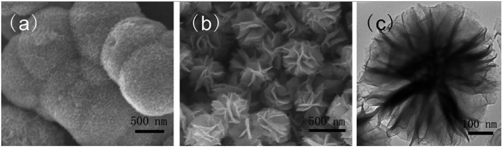 | ||
| Fig. 1 SEM (a, b) and TEM (c) images of In2S3 with thiourea (a) and L-cysteine (b, c) as the additive. | ||
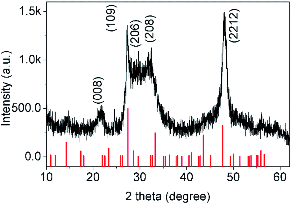 | ||
| Fig. 2 XRD pattern of the as-synthesized In2S3. | ||
:1.5, in accordance with the stoichiometric ratio in In2S3.
 | ||
| Fig. 3 XPS spectra of the as-synthesized In2S3: (a) a survey spectrum, (b) an In 3d spectrum, and (c) a S 2p spectrum. | ||
3.2 Synthesis of 3D CuInS2
3.2.1.1 The influence of the molar quantity of L-cysteine. Different morphologies of CuInS2 are shown in Fig. 4. They were synthesized with 3D In2S3 as the template, while the 3D In2S3 was obtained with different molar quantities of L-cysteine as the additive. When the molar quantity of L-cysteine is very low, only some irregular shaped crystals with a very small size in the large matrix could be seen (Fig. 4a). When the molar quantity of L-cysteine was increased to 3.0 mmol, some small hierarchical structured crystals with a size of no more than 100 nm could be seen; the hierarchical structure is assembled from nanosheets (Fig. 4b). When the molar quantity was increased to 4.5 mmol, a large sized 3D hierarchical walnut-shape structure of 400–500 nm formed, which is assembled from nanosheets (Fig. 4c), similarly to Fig. 4b. However, when the molar quantity was increased to 6.0 mmol, huge sized micrometer spheres formed with a size of 2–4 μm, but there are some small crystals adhering to the surface of the microspheres (Fig. 4d). Clearly, the molar quantity of L-cysteine played an important role in the formation of In2S3, leading to different morphologies of 3D CuInS2 being produced; that is, a low molar quantity of L-cysteine is not beneficial for the formation of 3D CuInS2, however, the addition of L-cysteine at a high molar quantity would result in the appearance of a heterogeneous crystal.
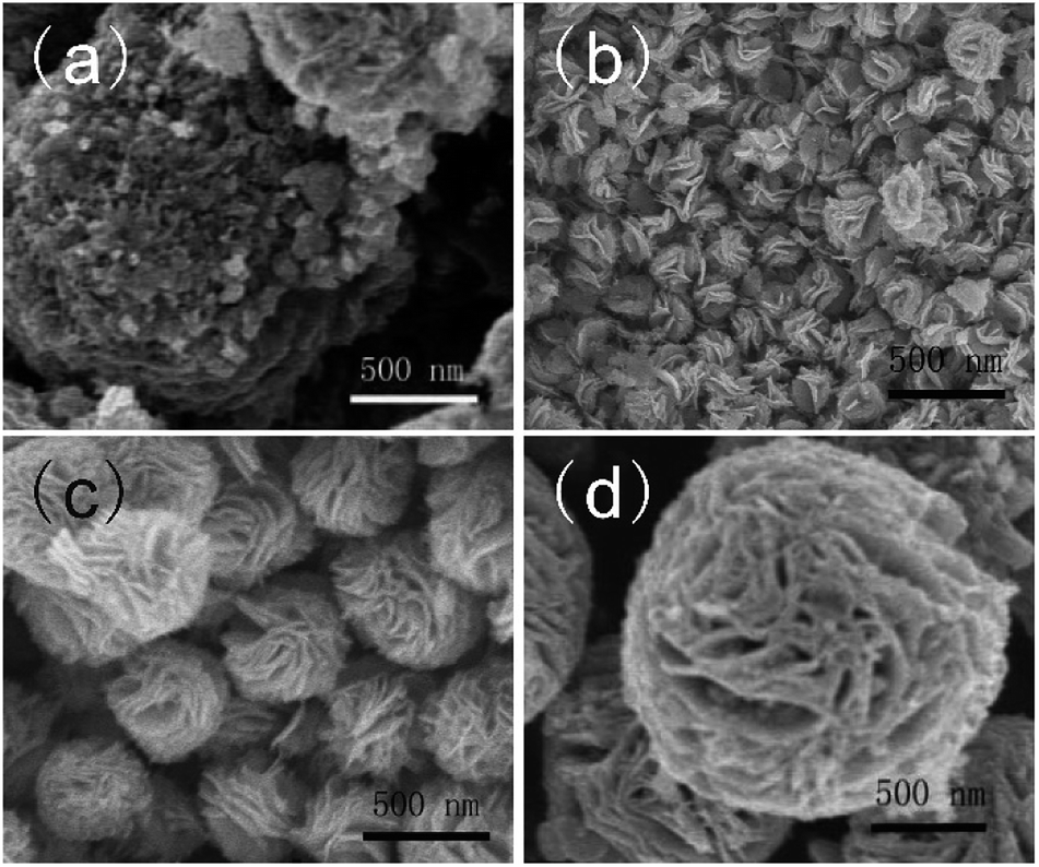 | ||
| Fig. 4 SEM images of CuInS2 synthesized with a molar quantity of L-cysteine of 1.5 mmol (a), 3.0 mmol (b), 4.5 mmol (c) and 6.0 mmol (d). | ||
3.2.1.2 The influence of different solvents. With the synthesized 3D In2S3 as the template, and with the cooperation of additional Cu2+, 3D In2S3 transforms to 3D CuInS2. In this step, the solvent plays an important role. Fig. 5 shows the influence of different solvents on the morphology of 3D CuInS2. Fig. 5a displays CuInS2 synthesized in aqueous solution; huge spheres with a size of about 5–6 μm could be observed, along with the presence of many fragmentary particles. However, in glycol solvent, smaller spheres with a size of 0.8–1 μm could be seen, which were assembled from many flakes (as shown in Fig. 5b). When CuInS2 was synthesized in DMF solvent (Fig. 5c), the SEM image shows that the products are walnut-shape 3D microspheres with diameters ranging from 400–600 nm, which are constructed from extremely developed hierarchical structures assembled from many interleaving and bending nanosheets. The flakes, aligned along different orientations, connected with each other to form a bunch, ultimately producing pinnacles at the centre of the hierarchical structure. Obviously, a change in solvent normally results in largely different morphologies of the products. DMF, as a strong coordinating solvent, is beneficial to the promotion of a 3D hierarchical structure. In a TEM image (Fig. 5d), particles with a size of about 500 nm could be seen clearly, with some obvious intervals existing between the adjacent nanosheets. The dark centre and pale perimeter of the product (shown in the inset of Fig. 5d) implied that the hierarchical structure is assembled in a compact manner at the centre, with very thin flakes along the perimeter.
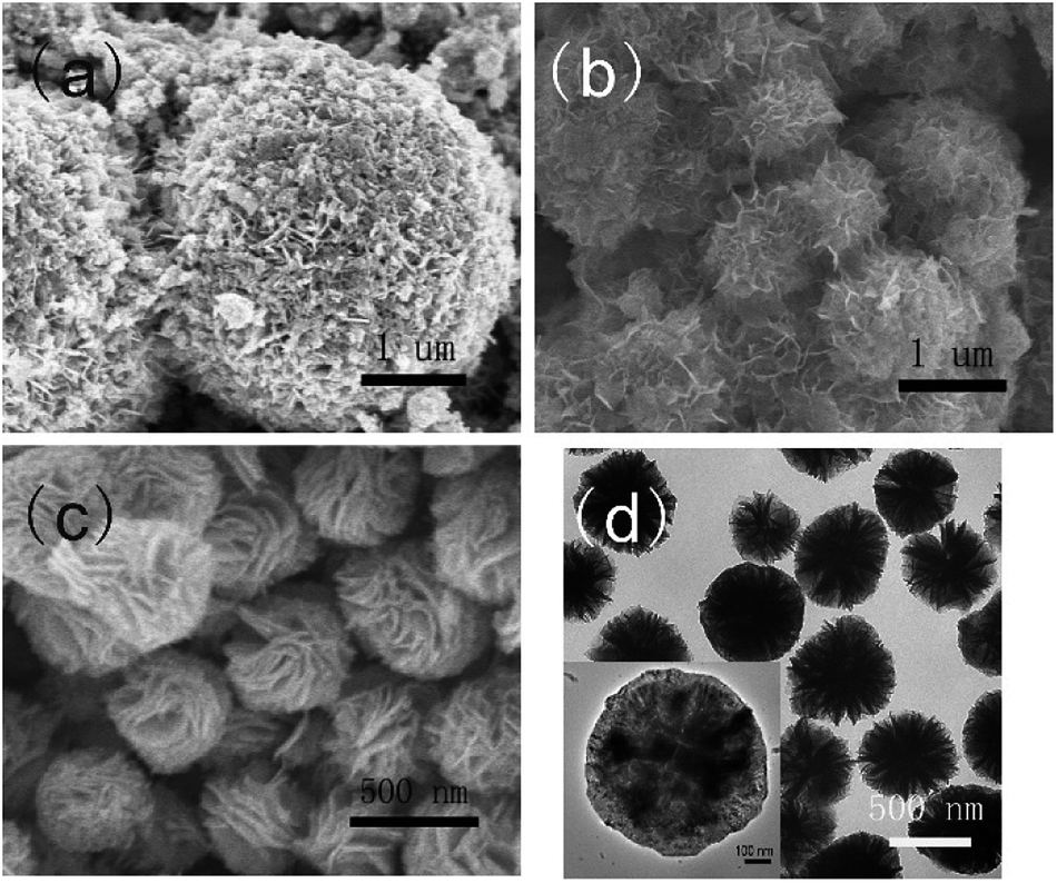 | ||
| Fig. 5 SEM (a–c) and TEM (d) images of CuInS2 with water (a), glycol (b) and DMF (c, d) as solvents. The inset of (d) is a single particle on a magnified scale. | ||
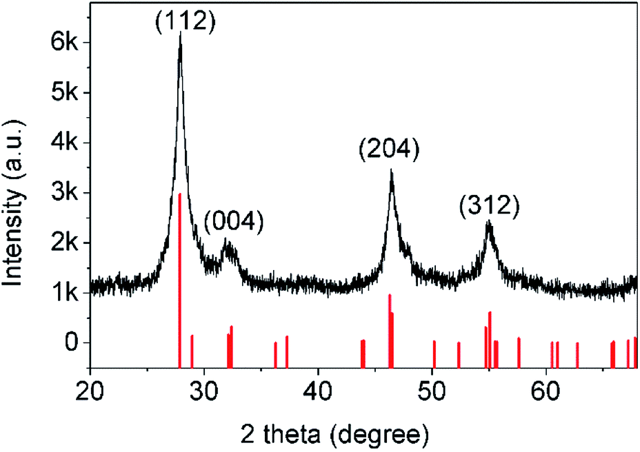
3.2.2.1 XRD analysis of CuInS2. Fig. 6 shows the XRD pattern of the obtained CuInS2 originating from In2S3, which was synthesized using 4.5 mmol of L-cysteine as the additive. Diffraction peaks at 2θ = 27.9°, 32.3°, 46.4° and 55.1° could be observed, which were assigned to the (112), (004), (204) or (220) crystal planes of CuInS2 with a chalcopyrite structure (a = b = 5.523 Å and c = 11.133 Å, JCPDS PCPDFWIN #85-1575).13b No impurity phase from In2S3 appeared, indicating that In2S3 transformed into CuInS2 completely.
 | ||
| Fig. 6 XRD pattern of the synthesized CuInS2. | ||
3.2.2.2 Raman spectrum of CuInS2. As a non-destructive characterization technique, a Raman scattering study could be applied to the analysis of CuInS2 powders prepared by a chemical route, to obtain the best possible crystalline CuInS2 in powder form.37 Fig. 7 shows the Raman spectrum of a CuInS2 powder sample. It may be observed that there are five peaks at 240, 263, 291, 319 and 340 cm−1 from the sample, which were assigned to the E, B2, A1, E and B2 modes of the chalcopyrite phase of CuInS2.38 The strong peak at 291 cm−1 may be assigned to the A1 mode, while the peak at 340 cm−1 may be assigned to the B2 mode.37 The Raman peak at 291 cm−1 was fitted to a Gaussian curve and the full-width at half-maximum (FWHM) was estimated to be 40.8 cm−1. Single crystal CuInS2 and almost defect free CuInS2 thin films were reported to have a FWHM of 3.5 and 5 cm−1, respectively.39 Compared to these values, the FWHM of our sample was much higher, indicating that considerable surface defects existed in the synthesized CuInS2. Clearly, 3D CuInS2 synthesized via a solvothermal method could not obtain favorable crystallinity.
 | ||
| Fig. 7 Raman spectrum of the synthesized CuInS2. | ||
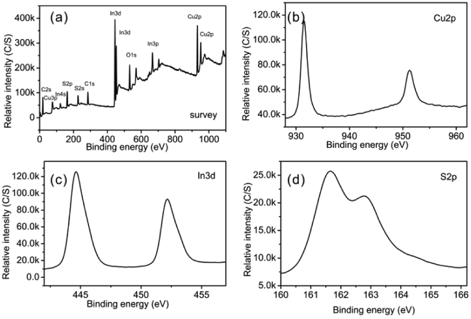
3.2.2.3 XPS analysis of CuInS2. Fig. 8 shows XPS spectra of CuInS2. From the survey spectrum (Fig. 8a), we could identify the existence of Cu, In, S, C and O. Similarly to the previous XPS data from In2S3, the presence of C and O is probably due to the presence of L-cysteine covering on the product and atmospheric contamination. The core level of the Cu 2p spectrum is split into Cu 2p3/2 (931.5 eV) and Cu 2p1/2 (951.3 eV) (Fig. 8b), in accordance with Cu+, but largely different from Cu 2p3/2 of Cu2+ (centred at 942 eV).40 Obviously, Cu in CuInS2 exists in the form of Cu+; Cu2+ as the reactant has been reduced by S2−, which originated from the decomposition of L-cysteine during the reaction. Similarly to the XPS pattern of In2S3, there are In 3d5/2 and In 3d3/2 peaks at 444.65 eV and 452.2 eV in the 3d spectrum, respectively (Fig. 8c).28
 | ||
| Fig. 8 XPS spectra of the as-synthesized CuInS2: (a) a survey spectrum, (b) a Cu 2p spectrum, (c) an In 3d spectrum, and (d) a S 2p spectrum. | ||
Moreover, the peaks at 161.7 eV for Cu–S and 162.8 eV for In–S could be observed in the S 2p core level spectrum (Fig. 8d). They are separated by an energy difference of 1.1 eV, similar to that for CuInS2.41 The above XPS data agree well with previous results.42 The quantification results showed a stoichiometric ratio of Cu:In:S of 1:1.2:2.1, which is very close to that of CuInS2.
3.2.2.4 Absorption spectrum. The UV-vis absorption spectrum of 3D CuInS2 was measured at room temperature in an ethanol dispersion (Fig. 9); typically, a broad shoulder without an obvious peak is visible in the absorption profile with a tail nearly to 900 nm, displaying good light-harvesting properties in the UV-visible range, similar to previous reports.42b,43 Using the direct band gap method, that is, plotting the squared absorbance versus energy and extrapolating to zero (inset of Fig. 9),44 the band gap of 3D CuInS2 is evaluated to be ca. 1.7 eV. Compared to the band gap of 1.5 eV in bulk CuInS2, this is blue-shifted obviously, which originates from the nanostructure existing in 3D CuInS2, confirming the quantum size effect.
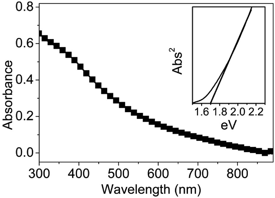 | ||
| Fig. 9 UV-vis absorption spectrum of 3D CuInS2; the inset is the determination of the band gap using the direct band gap method. | ||
Using 3D In2S3 as the template, additional Cu2+ and L-cysteine were added to synthesize 3D CuInS2. Cu2+ was reduced to Cu+ by S2− originating from L-cysteine,45 followed by the combination of 3D In2S3 and Cu+ to form 3D CuInS2. In this step, the solvent plays an important role in the morphology of 3D CuInS2. When the solvent is water, only irregular particles are produced (Fig. 5a). Water is the solvent with weak coordinating abilities; it could not combine Cu2+ effectively. Therefore, the additive Cu2+ ions were reduced to Cu+, and lots of Cu+ would combine with In2S3 instantly to form plenty of CuInS2 crystal nuclei and grow quickly, leading to the appearance of irregular particles. However, a glycol solvent displayed strong coordinating abilities, and could combine with Cu2+ to form the composite. Initially, some of the composite would be reduced and decomposed to produce Cu+. As Cu+ is consumed, that is, to combine with In2S3 to form CuInS2, Cu2+ would be released from the composite gradually and be reduced, which is beneficial for the formation of the 3D hierarchical structure. Moreover, DMF displayed stronger coordinating abilities, and could combine with Cu2+ tightly; only after the consumption of Cu2+ almost completely from the solution would it decompose to release Cu2+. Therefore, after the production of the initial CuInS2 nuclei, the slowing release of Cu2+ would result in oriented growth to form the large 3D hierarchical structure.
Obviously, in this experiment, L-cysteine displayed a strong tendency to coordinate with In3+, leading to In3+ and S2− being released slowly and decreasing the formation rate of In2S3, contributing to the formation of 3D In2S3. Furthermore, DMF as a strong coordinating solvent could combine with Cu2+ which would be reduced to Cu+. On the basis of 3D In2S3, Cu+ would combine with 3D In2S3 slowly, transforming to 3D CuInS2.
3.3 Solar cells
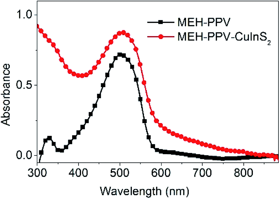 | ||
| Fig. 10 UV-vis absorption spectra of the composited film. | ||
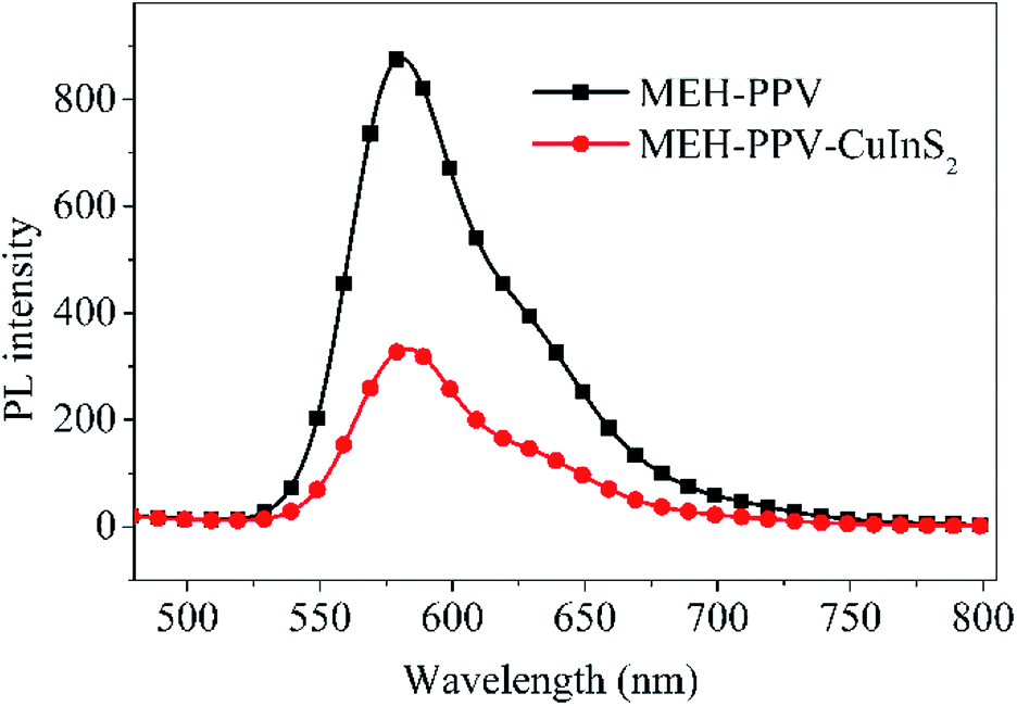 | ||
| Fig. 11 PL spectra of composited film. | ||
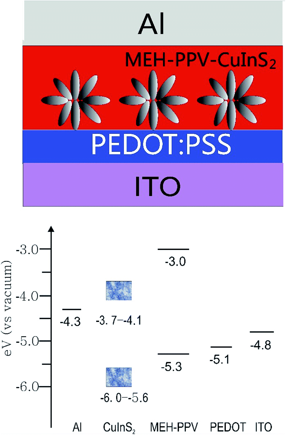 | ||
| Fig. 12 Device structure and energy level diagram for a MEH–PPV/3D CuInS2 solar cell. The data for ITO, PEDOT, MEH–PPV and Al are obtained by referring to ref. 13a and data for CuInS2 is obtained by referring to ref. 8c. | ||
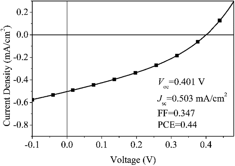 | ||
| Fig. 13 J–V curve of a MEH–PPV/3D CuInS2 solar cell. | ||
In comparison to our previous devices based on MEH–PPV and CuInS2 quantum dots (QDs),13a,b Jsc is much higher, which is due to the different electron transport method. In the previous device of MEH–PPV/CuInS2 QDs, QDs were distributed sporadically throughout the conjugated polymer film, making the charge transport via a hopping method between energy states, which is easily affected by defect sites existing in the photoactive layer. The presence of defect site would result in the charge recombination and discontinuous transport. Moreover, the randomly distributed MEH–PPV/CuInS2 interface normally leads to incomplete polymer PL quenching, particularly in the region which is more than the exciton diffusion length of the polymer away from the CuInS2 QDs.49 However, in the present device consisting of MEH–PPV and 3D CuInS2, 3D CuInS2 has a large active surface area, which would have high light scattering capacity.14 The large surface area and capacious interspaces (as shown in Fig. 5d) in the walnut-shape 3D structure offer more opportunities for the diffusion and mass transportation of MEH–PPV, contributing to the increased light-harvesting ability.50 On the other hand, the nanosheets in the 3D CuInS2 have very small thickness (only about 10–20 nm), which would promote charge transfer along straight pathways to the electrode, contributing to increased charge transport efficiency.51 Additionally, the increase in the charge-transfer rates drastically reduces the direct recombination of photogenerated electron–hole pairs, contributing to the higher charge collection efficiency.51 In conclusion, greater efficient light-harvesting ability, increased charge transport efficiency and the decreased recombination of the photogenerated electron–hole pairs contributed to the higher Jsc.
Compared to the previous device,13a Voc displayed different results depending on the surface state of 3D CuInS2. Voc is comparable to that of the device based on originally synthesized and untreated QDs, but is lower than that from surface-treated QDs. As we know, in HPSCs, the energy difference between the HOMO level of the donor (D) and the conduction band edge (CB) of the acceptor (A) determines Voc.52 In these two devices, the same D (MEH–PPV) and A (CuInS2) materials occupy almost the same HOMO and CB positions, therefore, the obviously different Voc may originate from other factors. Actually, it is mainly relevant to observe the quasi-Fermi level energy difference between electrons in the A and holes in the D.53 Voc in the present device is comparable to that of the previous device containing originally untreated CuInS2 QDs, which is due to the capping molecule L-cysteine covering on the surface of CuInS2 to produce more surface defects (as confirmed from the Raman spectrum), resulting in electrons being more easily trapped and accumulated in the lower quasi-Fermi levels than in the conduction band,54 leading to a low Voc.
It's noted that FF of the device is rather low. As we know, an important factor influencing the FF is the charge transport properties. According to a previous paper, the hole mobility (μh) of MEH–PPV and the electron mobility (μe) of CuInS2 are about 10−6 cm2 V−1 s−155 and 101 to 102 cm2 V−1 s−1;56 the larger difference between μe and μh would lead to the charge transport rate imbalance,57 contributing to the poor FF. Similar phenomena have been reported in a comparison of the device performance between PPV/PCBM device and P3HT/PCBM system. The μh of PPV derivative (10−5 to 10−6 cm2 V−1 s−1) is two or three orders of magnitude less than the μe of PCBM phase (10−3 cm2 V−1 s−1),58 but the μh of P3HT (10−4 cm2 V−1 s−1) is comparable to the μe of PCBM (10−3 cm2 V−1 s−1). As a result, in most devices, FF in PPV/PCBM device59 is much lower than that in P3HT/PCBM device.60 Additionally, the incompatible D/A interface may also result in the low FF. Normally, an inorganic material such as CuInS2 is hydrophilic, while an organic material such as MEH–PPV is hydrophobic, which would lead to serious incompatibility at the inorganic/organic interface, not favouring charge transfer between MEH–PPV and CuInS2. Moreover, the large amount of capping molecules covering on the surface of CuInS2 would impede electron transport, and the presence of considerable surface defects (as confirmed in the Raman spectrum) would cause much easier charge recombination of electron–hole pairs.61 All the above factors may result in the poor FF for the MEH–PPV/3D CuInS2 device.
In conclusion, we fabricate a MEH–PPV/3D CuInS2 device and obtain a PCE of 0.4%. The PCE is rather low compared to other PSCs with ZnO,2 TiO2,3 or CdSe4a as the acceptor, probably due to the poor crystallinity of CuInS2 synthesized via solvothermal methods. However, it is much higher than previous reports based on similarly structured devices based on CuInS2 nanoparticles,8b,c,13a,b suggesting that 3D CuInS2 is a promising structure when applied in HPSCs. It could be anticipated that, to obtain photovoltaic devices based on 3D CuInS2 with a higher power conversion efficiency, it is necessary to optimize the synthesis method to obtain CuInS2 with an ideal surface structure and better crystallinity, to apply surface modification to the inorganic and organic components, and to utilize Li salt doping to increase the hole mobility of MEH–PPV.
4. Conclusions
3D hierarchical micro/nanostructured CuInS2 was synthesized with pre-synthesized 3D In2S3 as the template. In the synthesis of In2S3, we found that 3D uniform flower-like β-In2S3 was synthesized successfully with the assistance of L-cysteine. Based on 3D In2S3, 3D CuInS2 could be synthesized successfully. The molar quantity of L-cysteine and the used solvent had important influences on the morphology of 3D CuInS2. When In2S3 was synthesized with 4.5 mmol of L-cysteine as the additive, with the cooperation of Cu2+ in DMF solution, walnut-shape 3D CuInS2 with a chalcopyrite structure was formed. We consider that the formation of 3D CuInS2 may originate from the strong coordinating effects of L-cysteine and DMF, which would lead to slow ion release and oriented crystal growth. CuInS2 displayed a wide absorption range in the UV-vis spectrum, and it could increase the absorption ability of a MEH–PPV–CuInS2 composite film and quench the PL of MEH–PPV effectively. As a result, 3D CuInS2 was used to fabricate MEH–PPV/3D CuInS2 solar cells, obtaining a PCE of 0.4%. The high Jsc value may result from the hierarchical structure, with a large active surface area and capacious interspaces, being beneficial to the penetration of MEH–PPV, and it could afford an effective path for electron transport and collection, while the low Voc may originate from plenty of capping molecules covering on the surface of CuInS2. The successful fabrication of MEH–PPV/3D CuInS2 solar cells suggests that 3D CuInS2 may be an effective electron acceptor for efficient HPSCs in the future.Acknowledgements
This work was supported by the International Cooperation Project of Anhui Province (1503062018), the Visiting Research Scholar Project for Young/Middle Excellent Talents of Anhui Province (gxfxZD2016110), the Preeminent Youth Foundation of Anhui Polytechnic University (2016JQ002) and the National Undergraduate Innovation Entrepreneurship Project in Local University (201510363085, 2016103630052).Notes and references
- (a) N. S. Sariciftci, L. Smilowitz and F. W. A. J. Heeger, Science, 1992, 258, 1474 CAS; (b) G. Yu, J. Gao, J. C. Hummelen, F. Wudl and A. J. Heeger, Science, 1995, 270, 1789 CAS.
- W. J. E. Beek, M. M. Wienk and R. A. J. Janssen, Adv. Funct. Mater., 2006, 16, 1112 CrossRef CAS.
- P. A. v. Hal, M. M. Wienk, J. M. Kroon, W. J. H. Verhees, L. H. Slooff, W. J. H. v. Gennip, P. Jonkheijm and R. A. J. Janssen, Adv. Mater., 2003, 15, 118 CrossRef.
- (a) W. U. Huynh, J. J. Dittmer and A. P. Alivisatos, Science, 2002, 295, 2425 CrossRef CAS PubMed; (b) A. P. Alivisatos, Science, 1996, 271, 933 CAS.
- N. C. Greenham, X. Peng and A. P. Alivisatos, Phys. Rev. B: Condens. Matter Mater. Phys., 1996, 54, 17628 CrossRef CAS.
- (a) S. A. McDonald, G. Konstantatos, S. Zhang, P. W. Cyr, E. J. D. Klem, L. Levina and E. H. Sargent, Nat. Mater., 2005, 4, 138 CrossRef CAS PubMed; (b) S. Günes, K. P. Fritz, H. Neugebauer, N. S. Sariciftci, S. Kumar and G. D. Scholes, Sol. Energy Mater. Sol. Cells, 2007, 91, 420 CrossRef.
- D. Cui, J. Xu, T. Zhu, G. Paradee, S. Ashok and M. Gerhold, Appl. Phys. Lett., 2006, 88, 183111 CrossRef.
- (a) E. Arici, D. Meissner and N. S. Sariciftci, Encyclopedia of Nanoscience and Nanotechnology, ed. H. S. Nalwa, 2004, vol. 3, p. 929 Search PubMed; (b) M. Piber, T. Rath, T. Grieber, G. Trimmel, F. Stelzer and D. Meissner, 2006 IEEE 4th World Conference on Photovoltaic Energy Conversion, 2006, vol. 1, p. 247 Search PubMed; (c) E. Arici, N. S. Sariciftci and D. Meissner, Adv. Funct. Mater., 2003, 13, 165 CrossRef CAS.
- (a) M. A. Green, K. Emery, D. L. King, S. Igari and W. Warta, Prog. Photovoltaics, 2002, 10, 355 CrossRef CAS; (b) H. J. Lewerenz, H. Goslowsky, K.-D. Husemann and S. Fiechter, Nature, 1986, 321, 687 CrossRef CAS.
- B. Tell, J. L. Shay and H. M. Kasper, Phys. Rev. B: Solid State, 1971, 4, 2463 CrossRef.
- (a) M. Afzaala and P. O'Brien, J. Mater. Chem., 2006, 16, 1297 RSC; (b) H. J. Lewerenz, Sol. Energy Mater. Sol. Cells, 2004, 83, 395 CrossRef CAS; (c) R. Klenk, J. Klaer, R. Scheer, M. C. Lux-Steiner, I. Luck, N. Meyer and U. Rühle, Thin Solid Films, 2005, 480–481, 509 CrossRef CAS.
- D. C. Look and J. C. Manthuruthil, J. Phys. Chem. Solids, 1976, 37, 173 CrossRef CAS.
- (a) W. Yue, S. Han, R. Peng, W. Shen, H. Geng, F. Wu, S. Tao and M. Wang, J. Mater. Chem., 2010, 20, 7570 RSC; (b) W. Yue, M. Lan, G. Zhang, W. Sun, S. Wang and G. Nie, Mater. Sci. Semicond. Process., 2014, 24, 117 CrossRef CAS; (c) W. Yue, F. Wu, C. Liu, Z. Qiu, Q. Cui, H. Zhang, F. Gao, W. Shen, Q. Qiao and M. Wang, Sol. Energy Mater. Sol. Cells, 2013, 114, 43 CrossRef CAS; (d) W. Yue, C. Liu, Z. Qiu and M. Wang, Sol. Energy, 2015, 113, 358 CrossRef CAS.
- F. Shao, J. Sun, L. Gao, S. Yang and J. Luo, ACS Appl. Mater. Interfaces, 2011, 3, 2148 CAS.
- L. Yu, Z. Li, Y. Liu, F. Cheng and S. Sun, Appl. Surf. Sci., 2014, 305, 359 CrossRef CAS.
- M. J. Bierman and S. Jin, Energy Environ. Sci., 2009, 2, 1050 CAS.
- (a) M. Liu, G. Li and X. Chen, ACS Appl. Mater. Interfaces, 2014, 6, 2604 CrossRef CAS PubMed; (b) C. Wen, X. Weidong, W. Juanjuan, W. Xiaoming, Z. Jiasong and L. Lijun, Mater. Lett., 2009, 63, 2495 CrossRef; (c) S. Peng, F. Cheng, J. Liang, Z. Tao and J. Chen, J. Alloys Compd., 2009, 481, 786 CrossRef CAS.
- (a) Q. A. Akkerman, A. Genovese, C. George, M. Prato, I. Moreels, A. Casu, S. Marras, A. Curcio, A. Scarpellini, T. Pellegrino, L. Manna and V. Lesnya, ACS Nano, 2015, 9, 521 CrossRef CAS PubMed; (b) W. van der Stam, A. C. Berends, F. T. Rabouw, T. Willhammar, X. Ke, J. D. Meeldijk, S. Bals and C. de Mello Donega, Chem. Mater., 2015, 27, 621 CrossRef CAS; (c) T. Kuzuya, Y. Hamanaka, K. Itoh, T. Kino, K. Sumiyama, Y. Fukunaka and S. Hirai, J. Colloid Interface Sci., 2012, 388, 137 CrossRef CAS PubMed; (d) V. Lesnyak, C. George, A. Genovese, M. Prato, A. Casu, S. Ayyappan, A. Scarpellini and L. Manna, ACS Nano, 2014, 8, 8407 CrossRef CAS PubMed.
- (a) L. Zheng, Y. Xu, Y. Song, C. Wu, M. Zhang and Y. Xie, Inorg. Chem., 2009, 48, 4003 CrossRef CAS PubMed; (b) D. Wu, J. Duan, C. Zhang, K. Guo and H. Zhu, J. Phys. Chem. C, 2013, 117, 9121 CrossRef CAS.
- H. Migge and J. Grzanna, J. Mater. Res., 1994, 9, 125 CrossRef CAS.
- S. Lei, C. Wang, L. Liu, D. Guo, C. Wang, Q. Tang, B. Cheng, Y. Xiao and L. Zhou, Chem. Mater., 2013, 25, 2991 CrossRef CAS.
- B. Chen, S. Chang, D. Li, L. Chen, Y. Wang, T. Chen, B. Zou, H. Zhong and A. L. Rogach, Chem. Mater., 2015, 27, 5949 CrossRef CAS.
- R. Diehl and R. Nitsche, J. Cryst. Growth, 1975, 28, 306 CrossRef CAS.
- Q. Lu, F. Gao and S. Komarneni, J. Am. Chem. Soc., 2004, 126, 54 CrossRef CAS PubMed.
- M. Valodkar, A. Pal and S. Thakore, J. Alloys Compd., 2011, 509, 523 CrossRef CAS.
- F. Chen, R. Zhou, L. Yang, M. Shi, G. Wu, M. Wang and H. Chen, J. Phys. Chem. C, 2008, 112, 13457 CAS.
- F. Gao, Q. Lu, X. Meng and S. Komarneni, J. Phys. Chem. C, 2008, 112, 13359 CAS.
- L.-Y. Chen, Z.-D. Zhang and W.-Z. Wang, J. Phys. Chem. C, 2008, 112, 4117 CAS.
- F. Zuo, S. Yan, B. Zhang, Y. Zhao and Y. Xie, J. Phys. Chem. C, 2008, 112, 2831 CAS.
- J. Jiang, R. Yu, R. Yi, W. Qin, G. Qiu and X. Liu, J. Alloys Compd., 2010, 493, 529 CrossRef CAS.
- J. Pan, S. Xiong, B. Xi, J. Li, J. Li, H. Zhou and Y. Qian, Eur. J. Inorg. Chem., 2009, 5302 CrossRef CAS.
- J. Xiang, H. Cao, Q. Wu, S. Zhang, X. Zhang and A. A. R. Watt, J. Phys. Chem. C, 2008, 112, 3580 CAS.
- S. Xiong, B. Xi, C. Wang, D. Xu, X. Feng, Z. Zhu and Y. Qian, Adv. Funct. Mater., 2007, 17, 2728 CrossRef CAS.
- S. Xiong, B. Xi, C. Wang, G. Zou, L. Fei, W. Wang and Y. Qian, Chem, 2007, 13, 3076 CrossRef CAS PubMed.
- X. Fu, X. Wang, Z. Chen, Z. Zhang, Z. Li, D. Y. C. Leung, L. Wu and X. Fu, Appl. Catal., B, 2010, 95, 393 CrossRef CAS.
- (a) N. Revathi, P. Prathap, Y. P. V. Subbaiah and K. T. Ramakrishna Reddy, J. Phys. D: Appl. Phys., 2008, 41, 155404 CrossRef; (b) S.-H. Yu, L. Shu, Y.-S. Wu, J. Yang, Y. Xie and Y.-T. Qian, J. Am. Ceram. Soc., 1999, 82, 457 CrossRef CAS.
- P. Guha, D. Das, A. B. Maity, D. Ganguli and S. Chaudhuri, Sol. Energy Mater. Sol. Cells, 2003, 80, 115 CrossRef CAS.
- K. Das, S. K. Panda, S. Gorai, P. Mishra and S. Chaudhuri, Mater. Res. Bull., 2008, 43, 2742 CrossRef CAS.
- J. Álvarez-García, J. Marcos-Ruzafa, A. Pérez-Rodríguez, A. Romano-Rodríguez, J. R. Morante and R. Scheer, Thin Solid Films, 2000, 361–362, 208 CrossRef.
- (a) J. Llanos, A. Buljan, C. Mujica and R. Ramfrez, J. Alloys Compd., 1996, 234, 40 CrossRef CAS; (b) L. D. Partain, R. A. Schneider, L. F. Donaghey and P. S. McLeod, J. Appl. Phys., 1985, 57, 5056 CrossRef CAS.
- J. F. Moulder, W. F. Stickle, P. E. Sobol and K. Bomben, X-Ray Data Booklet, Copyright 1992 by Perkin-Elmer Corp.: Physical Electronic Division, 1992 Search PubMed.
- (a) J. Xiao, Y. Xie, R. Tang and Y. Qian, J. Solid State Chem., 2001, 161, 179 CrossRef CAS; (b) D. Pan, L. An, Z. Sun, W. Hou, Y. Yang, Z. Yang and Y. Lu, J. Am. Chem. Soc., 2008, 130, 5620 CrossRef CAS PubMed.
- (a) H. Nakamura, W. Kato, M. Uehara, K. Nose, T. Omata, S. Otsuka-Yao-Matsuo, M. Miyazaki and H. Maeda, Chem. Mater., 2006, 18, 3330 CrossRef CAS; (b) H. Zhong, Y. Zhou, M. Ye, Y. He, J. Ye, C. He, C. Yang and Y. Li, Chem. Mater., 2008, 20, 6434 CrossRef CAS.
- Q. Guo, S. J. Kim, M. Kar, W. N. Shafarman, R. W. Birkmire, E. A. Stach, R. Agrawal and H. W. Hillhouse, Nano Lett., 2008, 8, 2982 CrossRef CAS PubMed.
- S. Han, M. Kong, Y. Guo and M. Wang, Mater. Lett., 2009, 63, 1192 CrossRef CAS.
- S.-S. Kim, J. Jo, C. Chun, J.-C. Hong and D.-Y. Kim, J. Photochem. Photobiol., A, 2007, 188, 364 CrossRef CAS.
- N. C. Greenham, X. Peng and A. P. Alivisatos, Phys. Rev. B: Condens. Matter Mater. Phys., 1996, 54, 17628 CrossRef CAS.
- (a) Y.-Y. Lin, T.-H. Chu, C.-W. Chen and W.-F. Su, Appl. Phys. Lett., 2008, 92, 053312 CrossRef; (b) Y. Y. Lin, T. H. Chu, S. S. Li, C. H. Chuang, C. H. Chang, W. F. Su, C. P. Chang, M. W. Chu and C. W. Chen, J. Am. Chem. Soc., 2009, 131, 3644 CrossRef CAS PubMed; (c) J. H. Warner, A. R. Watt, E. Thomsen, N. Heckenberg, P. Meredith and H. Rubinsztein-Dunlop, J. Phys. Chem. B, 2005, 109, 9001 CrossRef CAS PubMed.
- K. M. Coakley and M. D. McGehee, Chem. Mater., 2004, 16, 4533 CrossRef CAS.
- L. Feng, J. Jia, Y. Fang, X. Zhou and Y. Lin, Electrochim. Acta, 2013, 87, 629 CrossRef CAS.
- B. Li and Y. Wang, J. Phys. Chem. C, 2010, 114, 890 CAS.
- (a) S. Günes, H. Neugebauer and N. S. Sariciftci, Chem. Rev., 2007, 107, 1324 CrossRef PubMed; (b) M. Skompska, Synth. Met., 2010, 160, 1 CrossRef CAS; (c) T. Xu and Q. Qiao, Energy Environ. Sci., 2011, 4, 2700 RSC; (d) D. C. Olson, S. E. Shaheen, M. S. White, W. J. Mitchell, M. F. A. M. van Hest, R. T. Collins and D. S. Ginley, Adv. Funct. Mater., 2007, 17, 264 CrossRef CAS; (e) M. C. Scharber, D. Mühlbacher, M. Koppe, P. Denk, C. Waldauf, A. J. Heeger and C. J. Brabec, Adv. Mater., 2006, 18, 789 CrossRef CAS.
- (a) Y.-Y. Lin, T.-H. Chu, S.-S. Li, C.-H. Chuang, C.-H. Chang, W.-F. Su, C.-P. Chang, M.-W. Chu and C.-W. Chen, J. Am. Chem. Soc., 2009, 131, 3644 CrossRef CAS PubMed; (b) J. Bisquert and G. Garcia-Belmonte, J. Phys. Chem. Lett., 2011, 2, 1950 CrossRef CAS; (c) M. M. Lee, J. Teuscher, T. Miyasaka, T. N. Murakami and H. J. Snaith, Science, 2012, 338, 643 CrossRef CAS PubMed.
- (a) K. Schwarzburg and F. Willig, Appl. Phys. Lett., 1991, 58, 2520 CrossRef CAS; (b) G. Boschloo and A. Hagfeldt, J. Phys. Chem. B, 2005, 109, 12093 CrossRef CAS PubMed.
- (a) Q. Shi, Y. Hou, J. Lu, H. Jin, Y. Li, Y. Li, X. Sun and J. Liu, Chem. Phys. Lett., 2006, 425, 75 CrossRef; (b) M. H. Li, H.-L. Chen, Y.-F. Huang, W.-T. Chuang, Y.-R. Chen, H.-S. Tsai, O. A. Semenikhin and J. D. White, Chem. Phys. Lett., 2011, 505, 100 CrossRef CAS.
- (a) L. L. Kazmerski, M. S. Ayyagari and G. A. Sanborn, J. Appl. Phys., 1975, 46, 4865 CrossRef CAS; (b) Y. L. Wu and H. Y. Lin, Thin Solid Films, 1989, 168, 113 CrossRef CAS.
- D. Gupta, S. Mukhopadhyay and K. S. Narayan, Sol. Energy Mater. Sol. Cells, 2010, 94, 1309 CrossRef CAS.
- V. D. Mihailetchi, J. Wildeman and P. W. Blom, Phys. Rev. Lett., 2005, 94, 126602 CrossRef CAS PubMed.
- (a) M. T. Rispens, A. Meetsma, R. Rittberger, C. J. Brabec, N. S. Sariciftci and J. C. Hummelen, Chem. Commun., 2003, 17, 2116 RSC; (b) S. E. Shaheen, C. J. Brabec, N. S. Sariciftci, F. Padinger, T. Fromherz and J. C. Hummelen, Appl. Phys. Lett., 2001, 78, 841 CrossRef CAS; (c) T. Munters, T. Martens, L. Goris, V. Vrindts, J. Manca, L. Lutsen, W. D. Ceuninck, D. Vanderzande, L. D. Schepper, J. Gelan, N. S. Sariciftci and C. J. Brabec, Thin Solid Films, 2002, 403–404, 247 CrossRef CAS.
- G. Li, V. Shrotriya, J. Huang, Y. Yao, T. Moriarty, K. Emery and Y. Yang, Nat. Mater., 2005, 4, 864 CrossRef CAS.
- (a) A. Moliton and J.-M. Nunzi, Polym. Int., 2006, 55, 583 CrossRef CAS; (b) W. J. Potscavage Jr, A. Sharma and B. Kippelen, Acc. Chem. Res., 2009, 42, 1758 CrossRef PubMed.
| This journal is © The Royal Society of Chemistry 2017 |