
 Open Access Article
 This Open Access Article is licensed under a
 Creative Commons Attribution 3.0 Unported Licence
Marker patterning: a spatially resolved method for tuning the wettability of PDMS
N. Bodin-Thomazoab,
F. Malloggi *a and
P. Guenouna
*a and
P. Guenouna
aLIONS, NIMBE, CEA, CNRS, Université Paris-Saclay, CEA Saclay, 91191 Gif sur Yvette Cedex, France. E-mail: florent.malloggi@cea.fr
bInstitut Galien Paris-Sud, CNRS UMR 8612, 5 rue Jean-Baptiste Clément, 92290 Châtenay-Malabry, France
First published on 2nd October 2017
Abstract
Versatile, inexpensive and easy to use, PDMS has become a very common material, especially in the field of microfluidics. Intrinsically hydrophobic, it can be made hydrophilic by exposure to oxygen plasma. For some applications, wettability patterning of the PDMS surface is needed, in particular for the formation of monodisperse multiple emulsions. In this work we present an easy and spatially resolved way to tune the wettability of PDMS. Patterning is achieved without tedious or complicated surface processing by simply drawing the desired pattern onto the PDMS surface using the permanent ink of a marker as a masking layer. The microfluidic device is then exposed to oxygen plasma prior to bonding and flushed with ethanol when bonded. The parts of PDMS which are protected remained hydrophobic whereas unprotected surfaces are oxidized. The process is demonstrated by forming W/O/W emulsions in a controlled manner.
Introduction
For the last decades, studies devoted to polydimethylsiloxane (PDMS) have been considerably increasing. Easy to use, inexpensive, versatile and biocompatible, this intrinsically hydrophobic material exhibits numerous applications, especially in the field of microfluidics.However, in many applications, surface patterning of PDMS is needed to control wettability, like for the formation of a double emulsion in PDMS microfluidic chips. This kind of emulsions is very attractive in many fields like food, cosmetics or pharmaceutics, for the protection by encapsulation and controlled release of active principles1 or for the formation of capsules or core–shell particles.2–4 Microfluidics helps to control the inner encapsulation separately of the external phase and is invaluable for making monodisperse droplets. In order to form nicely isolated droplets in microfluidics, the internal liquid must not wet the walls of the channels. In the case of double emulsions this implies to make one part of the chip hydrophilic – to form oil-in-water droplets – and the other part hydrophobic – to form water-in-oil droplets. It is then a true challenge to find a simple and efficient way to pattern the wettability of PDMS surface.
Over the years, numerous methods have been developed to modify the surface properties of the PDMS and make it hydrophilic.5 The easiest way is the exposure to oxygen plasma.6 The siloxane groups of the surface are thus oxidized in silanols, making the surface hydrophilic. However, the effect of the oxidation only lasts for a couple of hours because of the migration of uncured low molecular weight PDMS oligomers from the bulk to the surface.7 Moreover, it is difficult to spatially control the latter oxidation to obtain a patterned surface.
To render the PDMS more durably hydrophilic, a wide range of surface modifications have been considered: dynamic surface modification by the adsorption of hydrophilic surfactants on the surface,8,9 layer-by-layer deposition of positively and negatively charged polyelectrolytes,10,11 surface modification via UV-polymerization12 of hydrophilic monomers on the walls of the channel or sol–gel methods.13 Although all these treatments are rather effective, they are in most cases time consuming and cumbersome to achieve, especially when wettability patterning is needed. In addition, the injection of several solutions and solvents into the microfluidic chip can induce contaminations or the introduction of dust leading to the clogging of the channels.
Very recently though, a couple of innovative easy ways to pattern the surface of PDMS without any chemical coating have appeared. Kim et al.14 used the property of the plasma treatment to oxidize first the areas close to the inlets of a hydrophobic bonded chip, playing with the oxygen ions diffusion gradient at short times. The plasma can thus be spatially controlled to achieve the oxidation of the targeted channels only, but a precise control of the geometry of the chip and of the plasma duration is needed. This method also requires to wait for the complete hydrophobic recovery of the channels after the plasma-bonding before using the chip.
In another paper, Li et al.15 developed a simple method to pattern the PDMS surface by masking the areas to be kept hydrophobic with epoxy glue during the plasma treatment. This method can be used in many geometries. However it requires to apply the glue precisely and to remove it after the plasma treatment without damaging the surface before the next step of bonding.
In this paper, we present a simple and versatile method to pattern the wettability of the PDMS and avoiding the potential previous difficulties. A permanent ink marker is used to mask the parts which need to remain hydrophobic during the plasma treatment, the latter ink being only removed by an ethanol flow after the bonding. This technique allows to pattern microchips with various geometries in a few minutes. To illustrate the method potentialities, we present one application of the chips formed by this method: the formation of water-in-oil-in-water (W/O/W) emulsions.
Moreover, to preserve the hydrophilicity due to the plasma treatment and the wettability pattern for a longer time, the chips can be stored in a freezer at −18 °C and be used to form multiple emulsion up to 5 days after the plasma treatment.
Materials and methods
Materials
Isopropyl myristate, ethanol, Tween®20 and Span®80 were obtained from Sigma Aldrich. Polylysine (20 kDa) grafted with polyethylene glycol (2 kDa) and labeled with fluorescein isothiocyanate (PLL-g-PEG/FITC) was purchased from Susos Surface Technology. All chemicals were used as received without further purification.PDMS Sylgard 184 and PDMS RTV 615 were purchased from Neyco (France). Photoresist SU8 was purchased from Chimie Tech Services (France). Silicon wafers were obtained from BT Electronics (France).
Markers used to pattern the wettability of the chips were black Stabilo© OHPen superfine, black Pilot SCA-UF© and red Simbalion© Extra Fine marking pens. Exact compositions of the inks are protected by patents and could not be obtained from the suppliers.
Device fabrication and patterning
Microfluidic channel patterns were fabricated by standard photolithography using SU8 photoresist spin-coated on a silicon wafer.16 Soft lithography was then used to replicate the channels: PDMS and its cross-linking agent were mixed at 10![[thin space (1/6-em)]](https://www.rsc.org/images/entities/char_2009.gif) :1 (w/w), degassed and cast on the mold. PDMS flat surfaces were made in the same way by casting the latter mixture in Petri dishes.
:1 (w/w), degassed and cast on the mold. PDMS flat surfaces were made in the same way by casting the latter mixture in Petri dishes.
The polymer was left curing for one night at 65 °C in an oven. PDMS chips were cut and peeled of the mold right before use, and 500 μm holes were punched into the polymer to create inlets and outlets.
To seal the channels, PDMS chip and a piece of flat PDMS were exposed for 2 min to oxygen plasma cleaner (Harrick scientific, USA) at 30 W and put in contact immediately after.
In case it is requested to keep some parts of the chip hydrophobic, the flat PDMS used to close the chip needs to be patterned as well to have fully hydrophobic channels, as it is presented in Fig. 1. To achieve this patterning before bonding, we protect the chip with tape and place PDMS flat on it. We can then draw a line onto the flat part in correspondence with the channel we want to keep hydrophobic. The tape is then removed and the channel itself is coated with the ink. After the plasma treatment is made, the chip and the flat PDMS are easily aligned thanks to the ink marking and bonded. As it can be seen in Fig. 2(b), marker lines are much wider than the channels, which makes the alignment easier. The marker inside the channel was rinsed by injection of ethanol after the bonding, until the outgoing solvent was clear. The chip was finally dried with nitrogen.
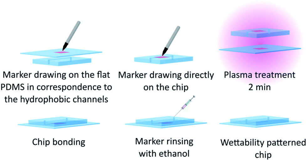 | ||
| Fig. 1 Successive steps for chip patterning with the marker technique. | ||
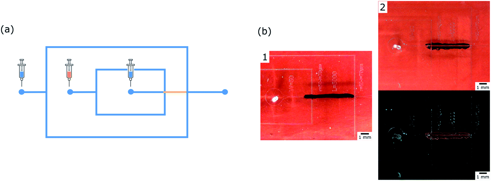 | ||
| Fig. 2 (a) Schematic representation of the chip geometry. Channels in blue were made hydrophilic by plasma treatment and channels in orange were kept hydrophobic. (b) Images of a chip 1-after bonding, 2-after rinsing: on the top the image with normal contrast, at the bottom a filtered picture (edge enhancement filter) which allows improving the visibility of the channels. | ||
If the wettability pattern needs to be preserved and used later on, the chip is placed in the freezer at −18 °C until use.
Contact angle measurement
Contact angle measurements were performed by deposing 10 μL water droplets on the substrate. Images of the droplets were taken with a camera and the angles determined thanks to the Image J Plugin Drop Analysis. Error bars were obtained from the different adjustments we performed on each image.In case of aging measurement, each measurement is performed on a new piece of PDMS (stored in a clean Petri dish) i.e. no multiple measurements on the same surface in order to prevent contaminations.
Characterization of the wettability of the surface
After rinsing the permanent marker with ethanol, PDMS was dried and PLL-g-PEG/FITC solution was placed on the plasmated PDMS or injected with a syringe into the channels of a chip. PDMS was incubated for 8 min before being dried with nitrogen. During this time FITC adsorbed on the negatively charged plasmated surfaces, thanks to electrostatic interactions.17The fluorescent areas are then observed with an Olympus Fluoview FV1000 inverted confocal microscope. FITC was excited at 488 nm by a multi-argon LASER and emitted light was collected between 500 and 600 nm. Fluorescent areas reveal the oxidized parts.
Formation of double emulsions
We worked with two successive cross junctions geometry to form our emulsions (see Fig. 2(a)). Channels were 100 μm wide and 50 μm high. The channel between the two junctions was kept hydrophobic during plasma treatment.Immediately after rinsing and drying, the chip was connected to glass syringes loaded with deionized water for the internal water phase, 3.5 w/w% Span®80 isopropyl myristate for the oil phase and with 0.1 or 0.7 w/w% Tween®20 water for the external water phase. Liquids were injected with various flow rates, the flow management inside the microfluidic system being performed by syringe pumps from neMESYS, Cetoni.
Typically, the flow rates are 0.5–2 μL min−1 for the internal water phase, 5–10 μL min−1 for the oil and 15–25 μL min−1 for the external water phase. The flow rates were adjusted to encapsulate exactly one water droplet in each oil globule.
Results
Surface wettability patterning
To go a step further, we investigated the influence of the time of plasma treatment on the wettability of the surface (Fig. 3). After 30 min of exposition the ink barrier is still efficient and the PDMS surface stays hydrophobic with a contact angle around 100°. However, the longer is the exposure, the higher the contact angle in the unprotected areas. This is due to the progressive appearance of cracks on the surface of PDMS at long oxidation times18 which increases the surface roughness.
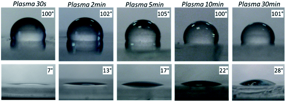 | ||
| Fig. 3 Evolution of the contact angle between water and PDMS as a function of the oxidation time: at the top in the areas protected by the ink, at the bottom in the unprotected areas. | ||
In this paper three different markers have been used: black Stabilo© OHPen superfine, black Pilot SCA-UF© and red Simbalion© Extra Fine marking pens. In general, every pen able to write properly on PDMS and therefore to form an homogeneous barrier to plasma ions can be used. Interestingly for the same brand this capacity depends on the color of the pen: for example red or blue Stabilo© OHPen were tested but could not write properly on the surface. Unfortunately no information could be obtained from the suppliers about the differences between the inks.
The effect of this ink masking technique was also tested on two other materials widely used in microfluidics: glass and Cyclic Olefin Copolymer (COC) (Table 1).
| Material | Contact angle before exposure to plasma | Contact angle after plasma treatment in the unprotected areas | Contact angle after plasma treatment in the protected areas |
|---|---|---|---|
| PDMS | 100° ± 8° | 13° ± 3° | 102° ± 7° |
| Glass | 19° ± 3° | ∼0° | 20° ± 3° |
| COC | 86° ± 7° | 53° ±4° | 80° ± 5° |
Glass is intrinsically hydrophilic when thoroughly cleaned, and will remain as such after a plasma treatment. Using glass we could thus check that the masked areas are still hydrophilic after rinsing the marker, meaning that the ink has a real protective effect and is not the source of the hydrophobicity observed in the protected areas for PDMS.
COC, on the contrary, is a lot more hydrophobic, and its surface is not as affected by the plasma than PDMS. Nevertheless protected COC appears to be more hydrophobic than the unprotected one.
After plasma treatment, PDMS surface is negatively charged, and the polylysine (PLL), positively charged, can be adsorbed onto the oxidized surface by electrostatic interactions.17 Thanks to the presence of the fluorescent molecule FITC on the chain, the oxidized areas are fluorescent.
Right after the plasma treatment, the ink was rinsed with ethanol and PDMS was incubated with a solution of PLL-g-PEG for 8 min and then dried. Fig. 4(a) shows that only the unprotected part of a piece of PDMS where dots were drawn appears fluorescent. This patterning technique is also used for a chip, as shown in the Fig. 4(b) and (c). Fluorescence is visible on the walls of the oxidized areas whereas no polymer was adsorbed on the masked areas.
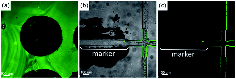 | ||
| Fig. 4 Confocal images of plasmated PDMS incubated with PLL-g-PEG/FITC. The marker areas were masked with permanent ink during the plasma treatment. (a) Image of a dot drawn on PDMS with permanent marker. (b) Channels of a patterned chip observed in direct light and fluorescence, (c) the fluorescence only. No FITC was adsorbed on the masked areas. | ||
Formation of W/O/W double emulsions
The formation of W/O/W emulsions in a unique chip is challenging because of the necessity to pattern the wettability of the channels. Indeed, the stability of water droplets requires hydrophobic walls whereas oil droplets require the walls to be hydrophilic.Thanks to the marker masking method such a patterning is easily made on the surface of the PDMS, making possible the formation of double emulsions.
The first junction and the channel joining the two intersections were masked by the permanent marker before plasma treatment. The flat PDMS used to close the chip was masked in correspondence. After the plasma treatment is made, the chip and the flat PDMS were easily aligned thanks to the ink marking and bonded, and the ink was rinsed by injecting ethanol inside the chip. It is worth noting that the marker is removed after the bonding preventing any risk to affect the hydrophilicity of the surface. The first junction and the intermediate channel, masked with marker, remain hydrophobic and allows the formation of inverse emulsions, whereas the second junction was oxidized (hydrophilic) and allows the formation of oil-in-water droplets.
Fig. 5 shows that we could make monodisperse W/O/W emulsions, without wetting of the water droplets between the two junctions of the chip. The standard deviation is less than 1.2% for the inner diameters and less than 1.7% for the outer diameters (n = 28). These low values are in accordance with other standard deviations found in literature for the formation of double emulsions with T or cross junctions.14,19,20 Though the marker line is larger than the channels, no leakages were observed in the zone protected by the ink. We performed complementary experiments where the resistance of the bonding in the presence of the marker was tested by injecting water into a blocked straight channel. Part of the channel was masked by ink during the plasma treatment, then the chip was bonded and marker rinsed before injecting water with increasing pressures. No rupture of the bonding was observed up to 2 bars which corresponds to a flow rate of ∼600 μl min−1 i.e. far beyond the flow rates used in the present study. However a progressive delamination was observed in the marked zone but with no noticeable influence on the emulsion.
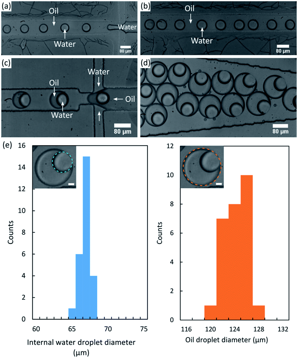 | ||
| Fig. 5 Formation of W/O/W emulsions in a chip patterned with permanent marker. (a) Formation of inverse emulsion at the first junction, (b) no wetting of the water droplets in the channels masked by the ink, (c) formation of W/O/W emulsion at the second junction, (d) multiple droplets in the exit chamber, (e) size distribution of the resulting double emulsion. | ||
In Fig. 6, we report the evolution of the inner droplets diameter as a function of internal water flow rate for two different oil flow rates and a fixed external water flow rate. As expected the droplets size can be tuned by varying the flow rates: keeping the oil and the external water phase flow rates constant, the higher the internal water phase flow rate, the higher the internal water droplet diameter, in agreement with what is reported in the literature.15,21,22 Accordingly, for given external and internal water phases flow rate, an increase of the oil phase flow rate leads to a decrease of the internal water droplet size.
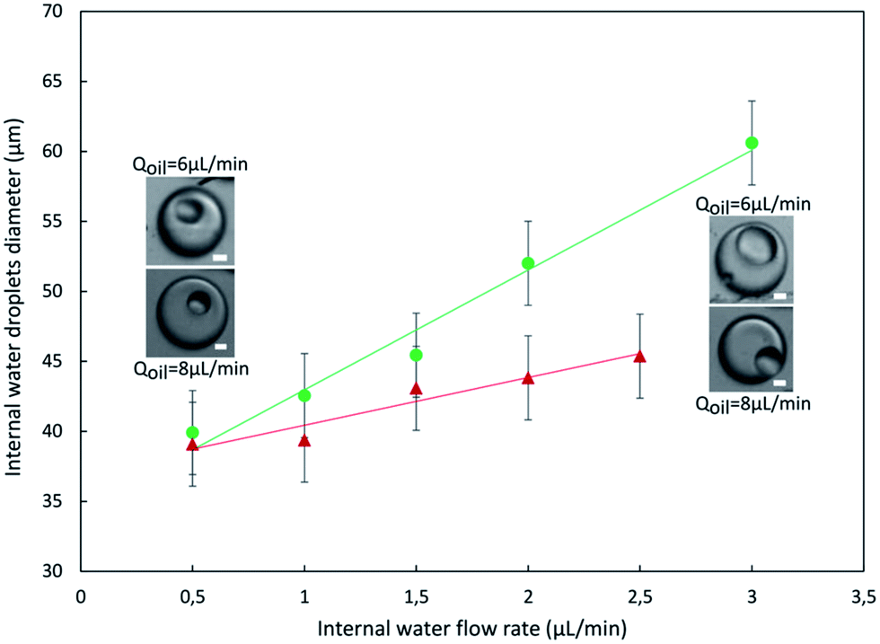 | ||
| Fig. 6 Evolution of the inner droplets diameter as a function of internal water flow rate, for Qexternal water = 25 μL min−1 and for two Qoil (●) = 6 μL min−1 and (▲) = 8 μL min−1. Insets: Optical microscopy images of the obtained droplets for the lowest and highest studied flow rates. Scale bars are 20 μm. | ||
Long-term hydrophilic stability
It is established that the hydrophilicity of the PDMS surface lasts only a couple of hours after being exposed to plasma, because of the migration of low molecular weight PDMS oligomers from the bulk of PDMS to the surface.Several methods have been developed to extend the effect of the plasma for several days. Lawton et al.23 showed that keeping the plasmated PDMS in water slows down the hydrophobic recovery of the surface. However, when exposed to air, the surface becomes hydrophobic again in a few hours.
Other methods allow to get rid of the low molecular weight oligomers. Eddington et al.,24 for example, used thermal aging to accelerate the migration of the oligomers and allow their evaporation. Regehr et al.25 exposed a method using a Soxhlet extraction in isopropanol, and Vickers et al.26 washed several times the PDMS in swelling solvents.
All these methods can be used before using the marker patterning. Following another approach, which is as simple as the marker patterning, we used the storage at −18 °C to preserve the hydrophilic properties of the chips once bonded. As mentioned earlier the migration of the uncured oligomers is sensitive to thermal diffusion and can be accelerated by heating the PDMS. Inversely, low temperatures slow down the migration of the small chains and the PDMS keeps its hydrophilic properties for a longer time.
Fig. 7 presents the evolution of the contact angle between plasmated PDMS and water in the air, compared to PDMS stored at ambient temperature and PDMS stored at −18 °C. The contact angle increases much faster for the PDMS stored at ambient temperature. After 5 days the contact angle is almost 60° whereas it is only 20° for the PDMS stored in freezer.
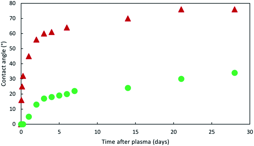 | ||
| Fig. 7 Evolution of air/plasmated PDMS/water contact angle as a function of time for PDMS plasmated at day 0 and store at room temperature (▲) or in a freezer (●). A new piece of PDMS is used for each measurement. | ||
Thanks to this storage method, we were able to form W/O/W in a patterned chip 5 days after exposure to plasma without wetting of the oil droplets (Fig. 8).
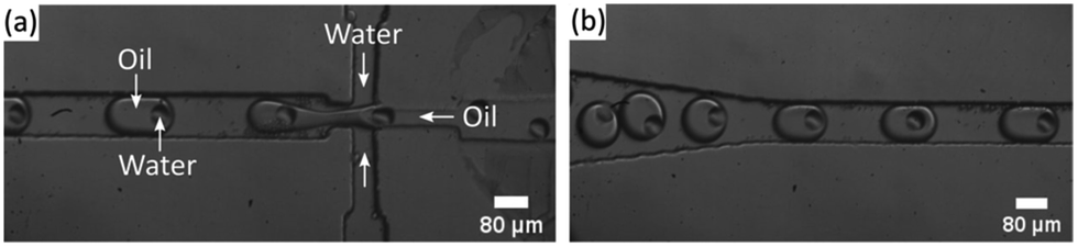 | ||
| Fig. 8 Formation of W/O/W emulsions in a chip plasmated five days before and stored at −18 °C before use. (a) Formation of water-in-oil-in-water droplets at the second junction, (b) no wetting of the oil droplets was observed. | ||
Discussion and conclusion
Although PDMS presents of lot of advantages, its intrinsic hydrophobicity can limit its utilization, even more when wettability patterning is needed. Several powerful methods have been developed to face this problem, but neither of them combine simplicity, rapidity and spatial resolution.Here we presented a very simple and versatile method to pattern the wettability of PDMS surface. The parts which were needed to be hydrophobic were simply masked with a permanent marker during the plasma treatment. Ink protects the surface against oxidation and can be rinsed easily with ethanol after the bonding, avoiding the possible alteration of the plasma.
The most difficult part of the bonding step could be the alignment of the chip on the flat PDMS, which is in our case facilitated by the visible marker lines in correspondence. Very few fails due to a misalignment were in fact observed.
The most common application of patterned PDMS is the formation of double emulsions, requiring some hydrophobic and hydrophilic parts on the same chip to form two kinds of droplets. In this article we focused on the formation of monodisperse W/O/W emulsions, but the formation of O/W/O emulsions or even more complicated structures can also be considered with the same technique, given that the protection of several channels on the same chip can be easily done.
More complex patterns as alternating hydrophobic and hydrophilic parts in the same channel are also possible. To be able to make very precise patterns at a higher resolution, the use of an ink-jet printer could be considered.
One of the major drawbacks of this method is the quick hydrophobic recovery of the PDMS after the oxidation, making the PDMS more and more hydrophobic and avoiding the formation of droplets. To cope with this problem, the patterning chips were stored in a freezer, slowing down the migration of the uncured oligomers and allowing to use a chip until 5 days after exposure to plasma.
Conflicts of interest
There are no conflicts to declare.Notes and references
- M. Leadi Cole and T. L. Whateley, J. Controlled Release, 1997, 49, 51–58 CrossRef.
- M. Windbergs, Y. Zhao, J. Heyman and D. A. Weitz, J. Am. Chem. Soc., 2013, 135, 7933–7937 CrossRef CAS PubMed.
- S.-H. Hu, S.-Y. Chen and X. Gao, ACS Nano, 2012, 6, 2558–2565 CrossRef CAS PubMed.
- P. Malo de Molina, M. Zhang, A. V. Bayles and M. E. Helgeson, Nano Lett., 2016, 16, 7325–7332 CrossRef CAS PubMed.
- I. Wong and C.-M. Ho, Microfluid. Nanofluid., 2009, 7, 291 CrossRef CAS PubMed.
- D. C. Duffy, J. C. McDonald, O. J. A. Schueller and G. M. Whitesides, Anal. Chem., 1998, 70, 4974–4984 CrossRef CAS PubMed.
- A. Tóth, I. Bertóti, M. Blazsó, G. Bánhegyi, A. Bognar and P. Szaplonczay, J. Appl. Polym. Sci., 1994, 52, 1293–1307 CrossRef.
- J. H. Xu, S. W. Li, J. Tan, Y. J. Wang and G. S. Luo, Langmuir, 2006, 22, 7943–7946 CrossRef CAS PubMed.
- J. H. Xu, G. S. Luo, S. W. Li and G. G. Chen, Lab Chip, 2006, 6, 131–136 RSC.
- G. Decher, Science, 1997, 277, 1232–1237 CrossRef CAS.
- W.-A. C. Bauer, M. Fischlechner, C. Abell and W. T. S. Huck, Lab Chip, 2010, 10, 1814–1819 RSC.
- S. Hu, X. Ren, M. Bachman, C. E. Sims, G. P. Li and N. L. Allbritton, Anal. Chem., 2004, 76, 1865–1870 CrossRef CAS PubMed.
- A. R. Abate, A. T. Krummel, D. Lee, M. Marquez, C. Holtze and D. A. Weitz, Lab Chip, 2008, 8, 2157–2160 RSC.
- S. C. Kim, D. J. Sukovich and A. R. Abate, Lab Chip, 2015, 15, 3163–3169 RSC.
- S. Li, X. Gong, C. S. M. Nally, M. Zeng, T. Gaule, C. Anduix-Canto, A. N. Kulak, L. A. Bawazer, M. J. McPherson and F. C. Meldrum, RSC Adv., 2016, 6, 25927–25933 RSC.
- Y. Xia and G. M. Whitesides, Angew. Chem., Int. Ed., 1998, 37, 550–575 CrossRef CAS.
- R. Marie, J. P. Beech, J. Vörös, J. O. Tegenfeldt and F. Höök, Langmuir, 2006, 22, 10103–10108 CrossRef CAS PubMed.
- B. Sarrazin, R. Brossard, P. Guenoun and F. Malloggi, Soft Matter, 2016, 12, 2200–2207 RSC.
- S. Okushima, T. Nisisako, T. Torii and T. Higuchi, Langmuir, 2004, 20, 9905–9908 CrossRef CAS PubMed.
- D. Saeki, S. Sugiura, T. Kanamori, S. Sato and S. Ichikawa, Lab Chip, 2010, 10, 357–362 RSC.
- W. Lee, L. M. Walker and S. L. Anna, Phys. Fluids, 2009, 21, 032103 CrossRef.
- T. Nisisako, S. Okushima and T. Torii, Soft Matter, 2005, 1, 23–27 RSC.
- R. A. Lawton, C. R. Price, A. F. Runge, W. J. Doherty III and S. S. Saavedra, Colloids Surf., A, 2005, 253, 213–215 CrossRef CAS.
- D. T. Eddington, J. P. Puccinelli and D. J. Beebe, Sens. Actuators, B, 2006, 114, 170–172 CrossRef CAS.
- K. J. Regehr, M. Domenech, J. T. Koepsel, K. C. Carver, S. J. Ellison-Zelski, W. L. Murphy, L. A. Schuler, E. T. Alarid and D. J. Beebe, Lab Chip, 2009, 9, 2132–2139 RSC.
- J. A. Vickers, M. M. Caulum and C. S. Henry, Anal. Chem., 2006, 78, 7446–7452 CrossRef CAS PubMed.
| This journal is © The Royal Society of Chemistry 2017 |