
 Open Access Article
 This Open Access Article is licensed under a
 Creative Commons Attribution 3.0 Unported Licence
Micro- and nano-patterns fabricated by embossed microscale stamp with trenched edges†
Jin-Hyun
Choi
,
Chang-Mok
Oh
and
Jae-Won
Jang
 *
*
Department of Physics, Pukyong National University, Busan 608-737, Korea. E-mail: jjang@pknu.ac.kr
First published on 23rd June 2017
Abstract
A submicron width of Au line patterns was fabricated from a polydimethylsiloxane (PDMS) line stamp of micron width by utilizing capillary-force and edge-transfer lithography (ETL). A template composed of Al(OH)3 was fabricated by capillary-force lithography (CFL) carried out by KOH ink-loaded microscale PDMS stamping on an Au nanomembrane (30 nm)-deposited Al thin layer (50 nm) on a glass substrate. Because the Au nanomembrane works as an OH− ion channel, protruding Al(OH)3 micro-structures are obtained by a pH-dependent molding process reacting underneath the Al thin layer. The protruding Al(OH)3 template has sharp edges at the molding area resulting from the capillary force working on the walls of the molding PDMS stamp and aqueous Al(OH)3 solution during the molding process. For example, the highest and widest ring edges of the protruding Al(OH)3 fabricated by a dot PDSM stamp (ϕ: 4.5 μm, gap: 3 μm) are obtained through a molding time of 20 min with 1 M KOH ink. The protruding Al(OH)3 micro-structures were used as templates to fabricate dot and line PDMS stamps. The replicated PDMS stamps have deep trenches around the contact area of the stamps; thus, the replicated PDMS stamp has an advantage of holding ink solution in the recessed space. Through (ETL) with a replicated line PDMS stamp, which has deep trenches around the line shape contact area, an Au line-pattern array of 700 nm in width was fabricated by 16-mercaptohexadecanoic acid (MHA) patterning on Au/Ti (30 nm/5 nm)-deposited silicon substrate and sequential Au etching for 20 min. In this study, we successfully demonstrated that an advantageous PDMS stamp for (ETL) is obtained by a solid Al(OH)3 template fabricated by Au nanomembrane-based CFL.
Introduction
The fabrication of nanoscale patterns using a microscale polydimethylsiloxane (PDMS) stamp is very attractive because users can obtain nanoscale patterns without using expensive lithographic tools, such as e-beam lithography1–5 and nanoimprint lithography.6–12 Regarding edge-transfer lithography (ETL)13,14 conducted with a microscale PDMS stamp, it has been reported that patterns with a much smaller size (sub-micron) than the PDMS stamp can be generated. In ETL, sub-micron patterns of inked molecules on the PDMS stamp are generated at the edges of the protruded patterns of the PDMS stamp. A key point of ETL is that the inked molecules on the PDMS stamp mainly transfer at the edge of the PDMS stamp, not at its contact area.13,14 For a successful ETL process, the inking of the molecules to be stamped should be loaded in the more recessed parts than the protruding parts (contact area) of the PDMS stamp. Silane molecule inking on a microscale PDMS stamp by discontinuous dewetting, which has an effect on the selective inking of silane molecules at only recessed parts of the PDMS stamp, was carried out to generate down to 90 nm-wide patterns.13 In addition, sub-micron (∼300 nm) patterns of alkanethiols were reported by surface modification of the PDMS stamp to obtain selective inking on the PDMS stamp. The selective inking of molecules only on the recessed part of the PDMS stamp is very important in sub-micron patterning in ETL.In this study, we develop a process to fabricate a PDMS stamp that is more suitable for conducting ETL; the PDMS stamp has deep trenches around its contact area to load more ink solution in its recessed part. In case of ETL with alkanethiol ink, additional treatment is required for the selective inking only on the recessed part of the PDMS stamp, due to absorption of alkanethiol inks into PDMS materials.14 Interestingly, the selective inking process is not necessary to carry out ETL with the PDMS stamp with trenches around the contact area. Moreover, as well as typical nanoscale contact printing, microscale printing is also available with the PDMS stamp with trenches. The PDMS stamp with trenches can transfer alkanethiol inks more densely at the edge than the contact area. Hence, two different alkanethiol self-assembled monolayers (SAMs) with different concentration can be generated. One is by typical microscale contact printing, the other is by ETL.
The PDMS stamp with deep trenches around the contact area was fabricated by a protruded Al(OH)3 template with sharp edges made from Au nanomembrane-based capillary-force lithography (CFL). In typical CFL, molding process by capillary-force working on recessed space of the stamp is a key phenomenon.15–17 Unlike most cases of CFL, inorganic materials can be molded with using Au nanomembrane as ion permeable channel.18 For example, protruded Al(OH)3 structures can be fabricated by a capillary-force assisting molding process conducted on an Au nanomembrane-deposited Al layer by a PDMS stamp.18 The edges of the protruded Al(OH)3 structures were tailored to be sharp by the capillary force working on the molded aluminum salt solution; thus, the sharp edges can be replicated as trenches when the PDMS stamp is fabricated by the protruded Al(OH)3 template. In the result, the sub-micron width of Au line patterns was obtained with ETL carried out with alkanethiol ink stamping by the replicated PDMS stamp on Au substrate and a sequential Au etching process. Originally, a line-shaped PDMS stamp (contact width: 10 μm, gap: 5 μm) was used to fabricate the protruded Al(OH)3 template by molding for 20 min with 1 M aqueous KOH ink, with which the line PDMS stamp (contact width: ∼9 μm, gap: ∼6 μm) was replicated and used in ETL for the fabrication of 700 nm-wide bi-lined Au patterns with 5 μm intervals and 15 μm of periodicity by stamping ethanolic 16-mercaptohexadecanoic acid (MHA) ink (10 mM) on an Au substrate (thickness: 30 nm) and sequential Au etching for 20 min. We successfully demonstrated that Au nanostructures (700 nm-wide lines) can be obtained originally from the microscle PDMS stamp of 10 μm in width. This methodology for fabricating a PDMS stamp with deep trenches around the contact area will be useful to conduct alkanethiol ink printing in ETL.
Experiments
Fabrication of PDMS stamp using Al(OH)3 template by Au nanomembrane-based CFL
As the first step, an Au nanomembrane (thickness: 30 nm)-coated Al film (thickness: 50 nm) on glass substrate was prepared by the thermal evaporation method (KVE-T2000, Korea Vacuum Tech., Korea). Two different dimensioned dot-array PDMS stamps (#1. hexagonal close packing (hcp) lattice, ϕ: 4.5 μm, gap: 3 μm, depth: 700 nm, #2. hcp lattice, ϕ: 4 μm, gap: 6 μm, depth: 700 nm) and a line PDMS stamp (width: 10 μm, gap: 5 μm, depth: 1 μm) with 1 M KOH ink solution (0.4 μl) were used for positive-tone Au nanomembrane-based lithography.18 For fabrication of the dot-array and the line PDMS stamps, hole-array and line silicon templates with the opposite dimension to the PDMS stamp were fabricated by photolithography (Korea Advanced Nano Fab Center, KOREA) and sequential reactive ion etching (RIE) process (Korea Advanced Nano Fab Center, KOREA). The silicon templates were cleaned by oxygen plasma for 2 min, and then overnight vapor coating of (heptadecafluoro-1,1,2,2-tetrahydrodecyl)trichlorosilane was carried out to make the surface of the Al(OH)3 templates hydrophobic. Resin and hardener for PDMS (Sylgard 184, Dow Corning, USA) with a mixture rate of 10![[thin space (1/6-em)]](https://www.rsc.org/images/entities/char_2009.gif) :1 (w/w) were poured on the Al(OH)3 templates, and the samples were baked in a convection oven (SH-VDO-30NH, SH Scientific, Korea) at 70 °C for 4 hours.19
:1 (w/w) were poured on the Al(OH)3 templates, and the samples were baked in a convection oven (SH-VDO-30NH, SH Scientific, Korea) at 70 °C for 4 hours.19
To obtain edge-tailored protruded Al(OH)3 micro-structures, a relatively thin Al layer (thickness: 50 nm), compared with typical positive-tone Au nanomembrane-based lithography,18 was used; non-sharp-edged protruded Al(OH)3 micro-structures were fabricated with a 100 nm Al layer underneath the Au nanomembrane. The positive-tone Au nanomembrane-based lithography was carried out with a molding time from 5 to 25 min. After the positive-tone Au nanomembrane-based lithography, the fabricated Al(OH)3 micro-structures were gently washed by de-ionized (DI) water. The fabricated Al(OH)3 micro-structures were characterized with a scanning electron microscope (SEM) (JXA-8530F, JEOL, JAPAN) and an atomic force microscope (AFM) (Dimension Icon, Bruker Co., USA). The sharp-edged protruded Al(OH)3 micro-structures obtained with the dot-array and line PDMS stamps were used as templates to fabricate PDMS stamps. The replicated PDMS stamps were fabricated by aforementioned procedure of PDMS stamp fabrication with using the Al(OH)3 templates as masters.
ETL for Au nano structure patterning using the PDMS stamp fabricated by CFL
ETL with the line PDMS stamp with trenches around the contact area fabricated by CFL was carried out on a thermally evaporated Au film (30 nm) with a Ti buffer layer (5 nm) on silicon substrate with ethanolic MHA ink (10 mM). Excessively loaded MHA ink solution on the PDMS stamp was removed by pre-printing several times on a sacrificial substrate in the printing process. Printed MHA-SAMs by the PDMS stamp worked as etching resist during the Au etching process carried out with aqueous Au etching solution containing 20 mM thiourea, 30 mM iron nitrate, 20 mM hydrochloric acid, and 2 mM 1-octanol.20–23 Rinsing with DI water and drying with N2 gas were carried out as the post-etching process of the samples. The Au nano/micro patterns fabricated by the ETL were characterized by an optical microscope (Axio Scope.A1, Carl Zeiss, Germany) and AFM (Dimension Icon, Bruker Co., USA).Results and discussion
CFL: fabrication of Al(OH)3 templates
According to our previous report,18 Au nanomembrane (30 nm-thick Au film) has pores of around 5 nm in diameter so that OH− ions can transfer through the Au nanomembrane. In the case of stamping KOH ink solution with a dot-array PDMS stamp on an Au nanomembrane-deposited Al layer, Al(OH)3 is molded in the space between the recessed part of the PDMS stamp and the Au nanomembrane (positive-tone Au nanomembrane nanolithography18). In Fig. 1(a), details of the molding process are displayed. The Au nanomembrane is thermally deposited on a 50 nm-thick Al film-coated glass substrate (Fig. 1(a)I). A sufficient volume (∼0.4 μl) of 1 M KOH ink is loaded on a PDMS stamp (i.e. dot-array stamp) to fully fill in recessed space of the PDMS stamp (Fig. 1(a)II). The KOH ink-loaded PDMS stamp is placed on the Au nanomembrane/Al film-coated glass substrate for 5–25 min to mold aluminum salt (Al(OH)3) in the recessed space of the PDMS stamp by utilizing the reaction between Al and KOH.18 (Fig. 1(a)III and 1(b)) As shown in Fig. 1(b), the main mechanism of the Al(OH)3 molding process is that as follows: the liquid phase of aluminum salt (Al(OH)4− (aq)) is formed by a reaction between the Al layer underneath the Au nanomembrane and OH− ions that have penetrated through the Au nanomembrane (eqn (1)), and the solid phase of aluminum salt (Al(OH)3 (s)) is obtained as the pH decreases in the liquid phase of aluminum salt18 (eqn (2)). Because the volume of the molding space (the volume of the recessed space of the PDMS stamp) is not sufficiently large, the pH decreases by consuming OH− ions in the reacting solution of the molding space.18 Finally, protruded Al(OH)3 patterns with opposite dimensions to the PDMS stamp can be obtained on the Au nanomembrane, as shown in Fig. 1(a)IV. Chemical reactions related to the molding process of Al(OH)3 are shown in eqn (1) and (2).24,25| 2Al (s) + 6H2O (l) + 2OH− (aq) → 2Al(OH)4− (aq) + 3H2 (g) | (1) |
| 2Al(OH)4− (aq) → 2Al(OH)3 (s) + OH− (aq) | (2) |
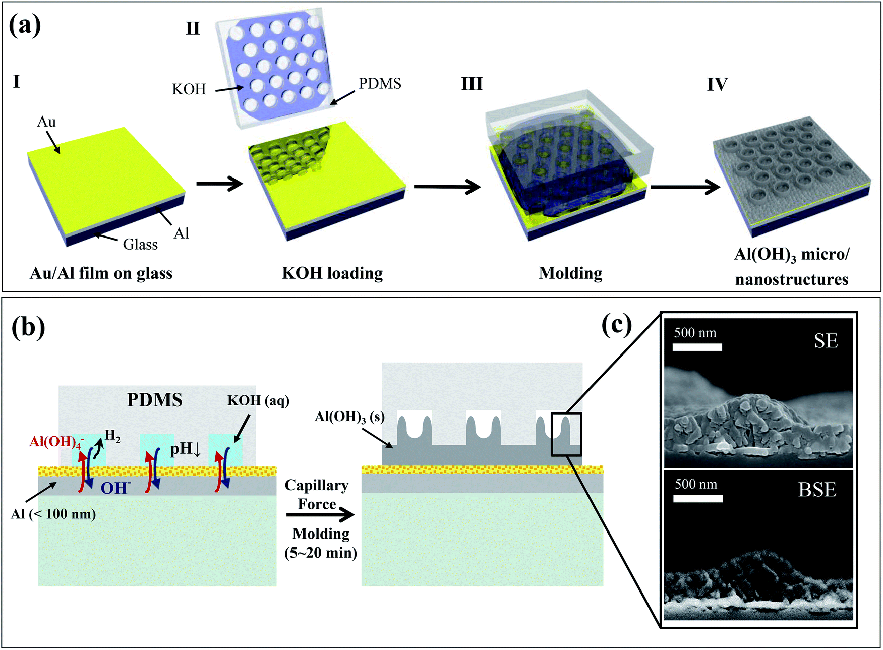 | ||
| Fig. 1 (a) Scheme for fabrication of Al(OH)3 template by a molding process (positive-tone Au nanomembrane-based nanolithography). (b) Mechanism of the Al(OH)3 molding process carried out with CFL (molding with a relatively thin Al layer). (c) Cross-sectional SEM images (SE and BSE) of the Al(OH)3 template; an edge of the template has been sharpened. | ||
The edges of the molded Al(OH)3 structures, which are protruded and have opposite dimensions to the PDMS stamp used in the molding process, can be tailored by using a relatively thin Al layer underneath the Au nanomembrane. In the case of CFL carried out on polystylene (PS) polymer spin-coated substrate with a PDMS stamp that is several micrometers (∼2.5 μm) deep, a relatively thin PS layer (thickness: ∼50 nm) has been used to form the molded PS structures with higher edges as a result of CFL.26 In our study, a relatively thin Al layer (<100 nm) compared with the depth of the PDMS stamp (700 nm) was also used to ensure the sharp edges of the molded Al(OH)3 micro-structures (Fig. 1(b)). If a dot-array PDMS stamp is used in the molding process with the thin Al layer underneath the Au nanomembrane, due to the sharp edges of the molded Al(OH)3 structures in the recessed space of the dot-array PDMS stamp, a ring-like Al(OH)3 structure array can be obtained, as shown in Fig. 1(a)IV. Fig. 1(c), cross-sectional SEM images of the ring-like Al(OH)3 structure, clearly shows that the edges of the molded Al(OH)3 micro-structures are tailored to be sharp. In addition, an approximately 200 nm-thick Al(OH)3 layer is also formed above the Au nanomembrane, and the Au nanomembrane is represented with high contrast in the back-scattered electron (BSE) mode SEM image (Fig. 1(c)). If KOH ink solution is not entirely removed from the contact of the PDMS stamp, aluminum salts could be solidified in the gap between the contact area of the PDMS stamp and the Au nanomembrane; thus, a thin Al(OH)3 layer would form above the Au nanomembrane, as shown in Fig. 1(b) and (c). The Al(OH)3 micro-structures with tailored edges fabricated by the molding process carried out with CFL can be used as templates to fabricate a PDMS stamp with specific dimensions derived from the tailored Al(OH)3 micro-structures.
The molding time dependence of Al(OH)3 micro-structures by CFL with a dot-array PDMS stamp (hcp lattice, ϕ: 4.5 μm, gap: 3 μm) is characterized in Fig. 2. To carefully characterize the dimensions of the molded ring-like Al(OH)3 micro-structures, the heights at the edge and center of the protruded ring-like Al(OH)3 micro-structures, respectively denoted as hedge and hcenter, as shown in Fig. 2(a), are measured by increasing the molding time from 5 min to 25 min. Fig. 2(a) shows a scheme of the cross-sectional dimensions of the molded ring-like Al(OH)3 micro-structures and how to determine hedge and hcenter of the Al(OH)3 micro-structures. The molding time-dependent hedge and hcenter are displayed in Fig. 2(b). Until 15 min, hedge and hcenter slightly increase to 50 nm with increases of the molding time. The hedge remarkably increases to 335 nm at 20 min of molding time and does not increase more (it seems to be saturated), whereas hcenter remarkably and gradually increases at the molding times of 20 min and 25 min. Because a ring-like shape can be observed at the edges of the protruded Al(OH)3 micro-structures, the dimensions of the ring, such as height (ring height) and width (ring width), are also measured as the molding time increases (Fig. 2(c)). In Fig. 2(d), it turns out that relatively high and thick ring structures are obviously measured in the molded Al(OH)3 micro-structures; topographic AFM images of the molding time-dependent Al(OH)3 micro-structures clearly show that obvious ring structures at the edges of the protruded Al(OH)3 micro-structures are fabricated in 20 min. The schematic images at the right side of Fig. 2(d) represent the cross-sectional structures of the molded Al(OH)3 at every molding time. Fig. 2(c) shows that the ring height and ring width decrease at the molding time of 25 min, which can be regarded as the Al(OH)3 starting to solidify near the walls of the PDMS stamp, then continuing to become solidified at the center of the recessed space of the PDMS stamp. The molding time-dependent cross-sectional schematic images of the Al(OH)3 structures are represented at the right side of Fig. 2(d). The edge of the molded Al(OH)3 micro-structures with a PDMS stamp can be tailored by properly adjusting the molding time; thus, the ring-like structure array of Al(OH)3 is obtained by 20 min of molding time with the dot-array PDMS stamp.
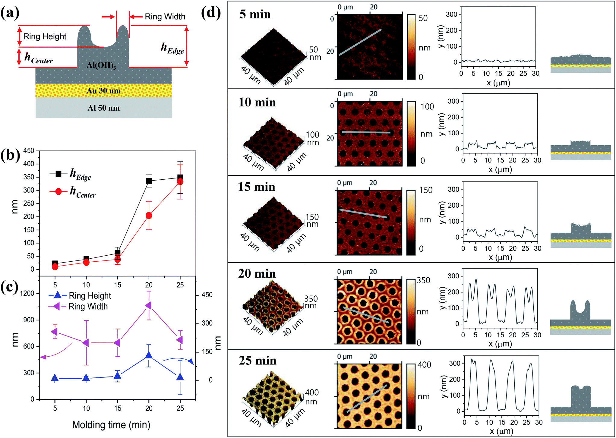 | ||
| Fig. 2 (a) Scheme of the Al(OH)3 micro-structures fabricated by the molding process. Parameters for dimensions of the Al(OH)3 micro-structures (hedge, hcenter, ring height, and ring width) are determined as displayed. (b, c) Graphs of molding time-dependent dimensional parameters of the Al(OH)3 micro-structures. (d) 3-Dimensional (3-D) and 2-dimensional (2-D) topological AFM images with cross-sectional line profile (obtained from the grey lines in 2-D topological AFM images) and scheme of the molding time dependent Al(OH)3 micro-structures. | ||
ETL: nano-patterning by the PDMS stamp obtained from the Al(OH)3 template
The edge-tailored Al(OH)3 micro-structure array can be used as a template for fabricating a PDMS stamp that is suitable for ETL. The sharp edge of the Al(OH)3 micro-structure can be transferred as a trench around the contact area of the replicated PDMS stamp, because a fabricated PDMS stamp by the Al(OH)3 micro-structure template has opposite dimensions. In Fig. 3(a), a scheme of fabrication of the replicated PDMS stamp from an Al(OH)3 template with a ring-like structure array is displayed. A ring-like Al(OH)3 micro-structure array fabricated by a hcp lattice dot-array PDMS with a 4 μm diameter and 6 μm gap is shown in Fig. 3(b), which was fabricated by 20 min of molding time with 1 M KOH ink solution. The fabricated ring-like Al(OH)3 micro-structure template shows that hedge, hcenter, ring height, and ring width are 0.32 μm, 0.21 μm, 0.13 μm, and 1.06 μm, respectively (Fig. 3(b)). As shown in Fig. 3(c), a dot-array PDMS stamp with a trench around its contact area was replicated by the Al(OH)3 micro-structure template. According to the AFM topographic image of the replicated PDMS stamp (Fig. 3(c)), the trenches of the replicated PDMS stamp show opposite dimensions to the ring shape of the Al(OH)3 template; the depth is 40 nm, and the width is 1.9 μm.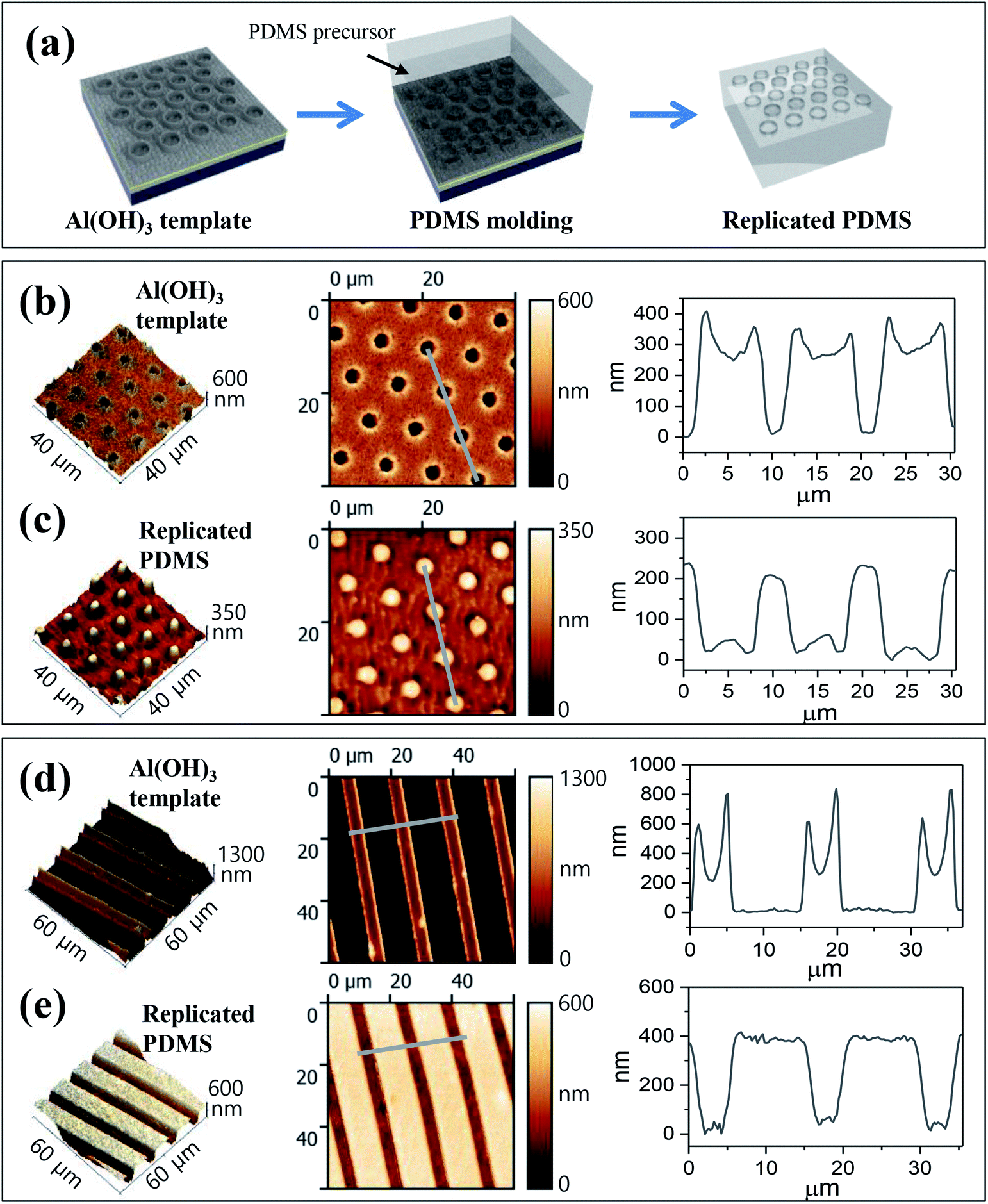 | ||
| Fig. 3 (a) Scheme of PDMS stamp replication from the Al(OH)3 template fabricated by CFL. (b–e) 3-D and 2-D topological AFM images and cross-sectional line profile: (b) a ring-like Al(OH)3 micro-structure array fabricated by a hcp lattice dot-array PDMS (ϕ: 4 μm, gap: 6 μm), (c) the replicated PDMS stamp by (b), (d) an edge-tailored line shape Al(OH)3 micro-structure template fabricated by a line-shaped PDMS stamp (width: 10 μm, gap: 5 μm), and (e) the replicated PDMS stamp by (d). The cross-sectional line profiles were measured from the grey lines in the 2-D topological AFM images. | ||
As well as the ring-like array Al(OH)3 micro-structure template (Fig. 3(b)), an Al(OH)3 micro-structure template fabricated by a line-shaped PDMS stamp (width: 10 μm, gap: 5 μm) was obtained (Fig. 3(d)) and used for fabricating the replicated PDMS stamp, as shown in Fig. 3(c) and (e). Similar to the replicated PDMS stamp with the ring-like Al(OH)3 micro-structure template, the sharp edges of the Al(OH)3 micro line array structured template (Fig. 3(d)) are transferred as trenches in the replicated line PDMS stamp (Fig. 3(e)). The replicated PDMS stamps have relatively smaller height of protruding part (contact area) than depth of the opposite dimensioned recessed space in the Al(OH)3 templates, which can be assumed to be due to the fact that the PDMS materials were not fully filled into the recessed space of the Al(OH)3 templates during the replication (Fig. S5†).
Trenches around the contact area of the ring and the line-shaped replicated PDMS stamp can work as reservoirs to hold more volume of an ink solution in the recessed space of the PDMS stamp; thus, the improved performance of the replicated PDMS stamp shown in Fig. 3(c) and (e) is expected when it is used in ETL. ETL carried out by the line-shaped replicated PDMS stamp is demonstrated in Fig. 4. MHA ink is used to pattern an Au film (30 nm) coated on glass substrate with a thin Ti buffer layer (5 nm), as shown in Fig. 4(a)I. During the printing process, MHA ink will be loaded more in the recessed space by the trenches around the contact areas, as shown in the schematic images of Fig. 4(a)I. Due to the larger volume of MHA ink on the trenches of the PDMS stamp than the contact area of the PDMS stamp, the more condensed MHA-SAMs will be patterned at the edges of the PDMS stamp rather than the center of the contact area of the PDMS stamp, as shown in the schematic images of Fig. 4(a)I and II. By means of two different densities of MHA-SAM patterns at the edge and center of the PDMS stamped area, the Au film will be sequentially etched in the following order: non-patterned area, the center of the MHA-SAM patterns, and the edge of the MHA-SAM patterns. Fig. 4(a)III and (b) show that only the Au film in the non-patterned area is removed for 10 min of Au etching time. When the etching time increases up to 20 min (Fig. 4(a)IV), the Au film underneath the center of the MHA-SAM patterns is also etched away; thus, the sub-micron width (∼700 nm) of the Au bi-lines is obtained, as shown in Fig. 4(c). The cross-sectional line profile shown in Fig. 4(b) represents that approximately 11 μm-wide and 35 nm-thick line patterns were obtained by 10 min of Au etching. Considering that the replicated line PDMS stamp (Fig. 3(e)) has approximately 9 μm-wide contact line patterns with an approximately 6 μm gap, it can be confirmed that MHA-SAMs were printed up to 1 μm away from the edges of the contact area of the line PDMS stamp. In addition, the MHA-SAMs printed at the outside edges of the line PDMS stamp work more efficiently as resist during the etching process until 20 min; the 35 nm-thick and approximately 700 nm-wide patterns were measured at the girth of the 11 μm-wide Au pattern, as is clearly shown in Fig. 4(c).
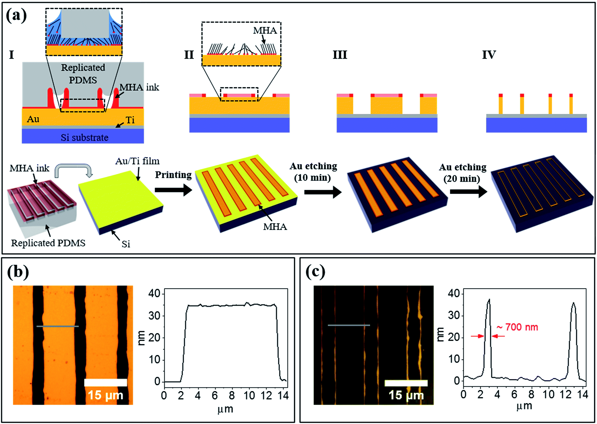 | ||
| Fig. 4 (a) ETL process carried out with the replicated PDMS stamp fabricated by the edge-tailored line shape Al(OH)3 micro-structure shown in Fig. 3(e). (I) MHA ink solution-loaded replicated PDMS is put on an Au/Ti film-deposited Si substrate. The short dashed box represents a detailed scheme of MHA-SAM formation at the contact of the PDMS stamp. (II) Relatively more condensed MHA-SAMs are printed at the edges of the contact area of the PDMS stamp. The short dashed box represents a detailed scheme of printed MHA-SAMs on the Au surface. (III) The printed MHA-SAMs work as etching resist with 10 min of Au etching. (IV) Only the relatively dense MHA-SAMs at the edges of the contact area work as etching resist with 20 min of Au etching. (b and c) Optical microscopic images and cross-sectional line profiles of the Au structures obtained from the ETL process of III (b) and IV (c), respectively. The cross-sectional line profiles were measured from the grey lines in the optical microscopic images. | ||
Conclusions
In conclusion, we have demonstrated that Au nanoscale line structures can be fabricated by the ETL process using a microscale line-shaped PDMS stamp replicated by an edge-tailored Al(OH)3 micro-structured template obtained by an Au nanomembrane-based CFL molding process (positive-tone nanolithography). In this study, a relatively thin Al layer (<100 nm) was introduced in Au nanomembrane-based positive-tone lithography18 for the molding of aluminum salt (Al(OH)3) with sharply tailored edge structures by the CFL process. It turns out that Al(OH)3 solidification starts from near the walls and continues in the center of the recessed space of the PDMS stamp used in the CFL process; for example, 20 min of molding time with 1 M KOH ink guarantees that the highest and widest ring edges of the protruded Al(OH)3 micro-structures can be fabricated by a dot PDSM stamp (ϕ: 4.5 μm, gap: 3 μm). Using the edge-tailored Al(OH)3 micro-structured template, an advantageous PDMS stamp for the ETL process could be fabricated; for example, ring-like and line-shaped PDMS stamps with trenches of ∼100 nm depth around the contact area were replicated from the edge-tailored Al(OH)3 micro-structured template fabricated by dot- and line-array PDMS stamps. As a result, 700 nm-wide Au bi-line structures (interval: ∼5 μm) were fabricated with MHA-SAM patterning and sequential Au etching by the microscale replicated line-shaped PDMS stamp (width: 9 μm, gap: 6 μm). Our demonstration will be a straightforward example of a relatively cheap methodology for fabricating sub-micron features using microscale PDMS stamp printing combined with Au nanomembrane lithography.Acknowledgements
This work was supported by a Research Grant of Pukyong National University (2016 Year).References
- Y. Chen, Microelectron. Eng., 2015, 135, 57–72 CrossRef CAS.
- Y. Chen, D. Macintyre and S. Thoms, J. Vac. Sci. Technol., B: Microelectron. Nanometer Struct.--Process., Meas., Phenom., 1999, 17, 2507–2511 CrossRef CAS.
- W. Hu, K. Sarveswaran, M. Lieberman and G. H. Bernstein, J. Vac. Sci. Technol., B: Microelectron. Nanometer Struct.--Process., Meas., Phenom., 2004, 22, 1711–1716 CrossRef CAS.
- Y. Ishii and J. Taniguchi, Microelectron. Eng., 2007, 84, 912–915 CrossRef CAS.
- J. Taniguchi, K. Koga, Y. Kogo and I. Miyamoto, Microelectron. Eng., 2006, 83, 940–943 CrossRef CAS.
- S. Y. Chou, P. R. Krauss and P. J. Renstrom, J. Vac. Sci. Technol., B: Microelectron. Nanometer Struct.--Process., Meas., Phenom., 1996, 14, 4129–4133 CrossRef CAS.
- M. M. Alkaisi and K. Mohamed, in Lithography, ed. M. Wang, InTech, Rijeka, 2010 Search PubMed.
- H. Lan and Y. Ding, in Lithography, ed. M. Wang, InTech, Rijeka, 2010 Search PubMed.
- D. Ye, P.-I. Wang, Z. Ye, Y. Ou, R. Ghoshal, R. Ghoshal and T.-M. Lu, Microelectron. Eng., 2010, 87, 2411–2415 CrossRef CAS.
- H. Lim, K.-B. Choi, G. Kim, S. Park, J. Ryu and J. Lee, Microelectron. Eng., 2011, 88, 2017–2020 CrossRef CAS.
- H. Hauser, B. Michl, V. Kübler, S. Schwarzkopf, C. Müller, M. Hermle and B. Bläsi, Energy Procedia, 2011, 8, 648–653 CrossRef CAS.
- N. Unno and J. Taniguchi, Microelectron. Eng., 2011, 88, 2149–2153 CrossRef CAS.
- O. Cherniavskaya, A. Adzic, C. Knutson, B. J. Gross, L. Zang, R. Liu and D. M. Adams, Langmuir, 2002, 18, 7029–7034 CrossRef CAS.
- R. B. A. Sharpe, B. J. F. Titulaer, E. Peeters, D. Burdinski, J. Huskens, H. J. W. Zandvliet, D. N. Reinhoudt and B. Poelsema, Nano Lett., 2006, 6, 1235–1239 CrossRef CAS PubMed.
- S.-H. Lee, H.-N. Kim, R.-K. Kwak and K. Y. Suh, Langmuir, 2009, 25, 12024–12029 CrossRef CAS PubMed.
- K.-Y. Suh, M. C. Park and P. Kim, Adv. Funct. Mater., 2009, 19, 2699–2712 CrossRef CAS.
- K. Y. Suh, Y. S. Kim and H. H. Lee, Adv. Mater., 2001, 13, 1386–1389 CrossRef CAS.
- C.-M. Oh, K. H. Park, J.-H. Choi, S. Hwang, H. Noh, Y. M. Yu and J.-W. Jang, Chem. Mater., 2017, 29, 3863–3872 CrossRef CAS.
- D. Qin, Y. Xia and G. M. Whitesides, Nat. Protoc., 2010, 5, 491–502 CrossRef CAS PubMed.
- D. A. Weinberger, S. Hong, C. A. Mirkin, B. W. Wessels and T. B. Higgins, Adv. Mater., 2000, 12, 1600–1603 CrossRef CAS.
- H. Zhang, R. Jin and C. A. Mirkin, Nano Lett., 2004, 4, 1493–1495 CrossRef CAS.
- X. Chen, G. Zheng, J. I. Cutler, J.-W. Jang and C. A. Mirkin, Small, 2009, 5, 1527–1530 CrossRef CAS PubMed.
- J.-W. Jang, R. G. Sanedrin, A. J. Senesi, Z. Zheng, X. Chen, S. Hwang, L. Huang and C. A. Mirkin, Small, 2009, 5, 1850–1853 CrossRef CAS PubMed.
- D. Belitskus, J. Electrochem. Soc., 1970, 117, 1097–1099 CrossRef.
- G. K. Schweitzer and L. L. Pesterfield, The Aqueous Chemistry of the Elements, Oxford University Press, New York, 2010 Search PubMed.
- Y. Cai, Z. Zhao, J. Chen, T. Yang and P. S. Cremer, ACS Nano, 2012, 6, 1548–1556 CrossRef CAS PubMed.
Footnote |
| † Electronic supplementary information (ESI) available: Capillary-force lithography without Au nanomembrane, cross-sectional SEM images of the molding time-dependent Al(OH)3 micro-structures, example of Al(OH)3 template fabrication: dependence on dimension of the PDMS stamp for molding, fill-in factor of the replicated PDMS stamps in the Al(OH)3 templates, edge-transfer lithography with replicated PDMS stamp by ring-shaped Al(OH)3 template, edge-transfer lithography with a normal line PDMS stamp (without trenches). See DOI: 10.1039/c7ra05262f |
| This journal is © The Royal Society of Chemistry 2017 |