DOI:
10.1039/C7RA05131J
(Paper)
RSC Adv., 2017,
7, 28494-28498
Investigation of the hole transport characterization and mechanisms in co-evaporated organic semiconductor mixtures
Received
7th May 2017
, Accepted 25th May 2017
First published on 30th May 2017
1 Introduction
In recent times, highly efficient organic optoelectronic devices1–8 have been obtained by using an organic heterojunction structure, including organic light emitting diodes (OLEDs) and organic solar cell (OSCs). As is well known, charge carrier transport is a crucial parameter affecting the performance of these devices. Furthermore, the systematic investigation of the charge transport characteristics in organic semiconductors is very important for establishing the relationship between the transport characteristics and device performance, and improving the performance of the devices. Therefore, it is necessary and desirable to study the transport characteristics in organic semiconductors. In contrast to the rapid progress made in the device performance, the understanding of the charge transport characteristics of the organic heterojunctions is still not clarified.
So far the charge carrier transport characteristics in organic semiconductors have been usually analyzed by several techniques, such as time of flight (TOF),9,10 transient electroluminescence (TEL),11,12 space charge limited current (SCLC)13–15 and admittance spectroscopy (AS).16–21 In these techniques, notably, AS has been shown to be a feasible and powerful tool to explore the charge carrier transport kinetics and relaxation processes and involved in optoelectronic devices. In addition, it is applicable to charge carrier transport characteristics of organic semiconductor film whose thickness is approximately comparable to that of practical devices. It can also be applied without the need for a complex experimental setup.
The 1,4,5,8,9 and 11-hexaazatriphenylene-hexacarbonitrile (HAT-CN) material has been drawing a great deal of attention because it has a lot of interesting characteristics.22–28 It has been adapted as the charge generation layer in some tandem OLEDs for higher power efficiency due to its very good electron affinity. It has also been used to modify metal surface electronic properties due to its unoccupied molecular orbital (LUMO) almost close to the Fermi level. However, there are rare reports about the study on HAT-CN organic mixtures by AS measurements. In this work, we systematically investigated the hole transport characteristics and mechanisms in the mixtures of HAT-CN![[thin space (1/6-em)]](https://www.rsc.org/images/entities/char_2009.gif) :NPB, HAT-CN:TAPC and HAT-CN:CBP by current density–voltage characteristics, AS technique, energy level analysis and atomic force microscopy.
:NPB, HAT-CN:TAPC and HAT-CN:CBP by current density–voltage characteristics, AS technique, energy level analysis and atomic force microscopy.
2 Experimental
The hole-only devices were fabricated on glass substrates pre-coated with a 180 nm-thick indium tin oxide (ITO) film with a sheet resistance of ∼10 Ω per square. Before the fabrication process, the ITO surface was thoroughly cleaned in an ultrasonic bath using subsequently detergents and deionized water, dried at 120 °C. The device structure was ITO/HAT-CN (10 nm)/HAT-CN:X (2:1, 180 nm)/HAT-CN (10 nm)/Al. Here, X was N,N′-di(naphthalene-1-yl)-N,N′-diphenyl-benzidine (NPB), 4,4′-cyclohexylidenebis[N,N-bis(4-methylphenyl)benze namine] (TAPC) and 4,4′-bis(carbazol-9-yl)-biphenyl (CBP), respectively. Structures of organic molecules are depicted in Fig. 1. All organic materials were grown in succession by thermal evaporation in a high-vacuum (∼4 × 10⁻⁴ Pa) without breaking vacuum. The Al electrodes were deposited on the substrates through shadow masks. The active area of device is 4 × 4 mm2. During the deposition process, the rate was controlled with quartz crystal oscillators and monitored by a frequency counter and calibrated by a Dektak 6 M profiler (Veeco).
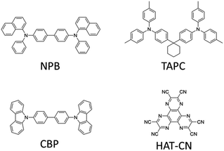 |
| | Fig. 1 Structures of organic molecules used in this work. | |
The current density–voltage (J–V) characteristics were carried out using a Keithley 2400 sourcemeter integrated with a vacuum cryostat (Optistat DN-V, Oxford Instruments). The admittance was measured at room temperature by an Agilent E4980A precision LCR meter in the frequency range of 20 Hz–13 MHz with the oscillation amplitude of the ac voltage kept at 100 mV. The morphologies of the thin films on ITO substrates were tested by atomic force microscopy (AFM) (SPA 400, Seiko Instruments Inc.).
3 Results and discussion
3.1 Current density–voltage characteristics
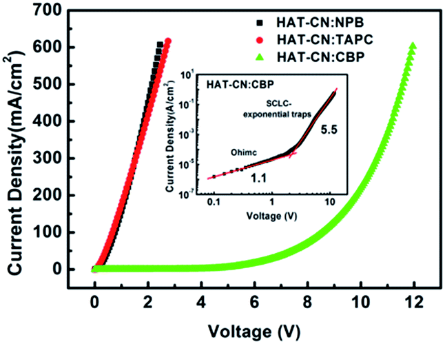
The J–V characteristics of the hole-only devices based on HAT-CN:NPB, HAT-CN:TAPC and HAT-CN:CBP mixtures are shown in Fig. 2. At a constant current density, the driving voltages of HAT-CN:NPB and HAT-CN:TAPC mixtures are close and lower, demonstrating the similar hole transport ability. In our previous work,29 the J–V characteristics of the two devices with different mixing concentration (y) have been discussed in detail. The results showed that their hole conductions (y < 90%) exhibit space-charge-limited current (SCLC) with free trap distributions. Conversely, it is shown a higher voltage for HAT-CN:CBP mixture. As shown in the inset, it clearly show two distinct regions: (1) ohmic region, the slope of logJ–logV curve is about 1.1 at the lower voltage region. (2) SCLC with exponential trap distribution region, the slope of J–V curve in double logarithmic is about 5.5 at higher voltages. For organic semiconductor devices, the charge carrier mobility plays a crucial role in determining the J–V characteristics.
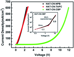 |
| | Fig. 2 The current–voltage characteristics of the hole-only devices based on HAT-CN:NPB, HAT-CN:TAPC and HAT-CN:CBP mixtures. Inset: the current–voltage characteristics for HAT-CN:CBP device in double logarithmic representation. | |
In order to clearly demonstrate the similarities and differences in the three hole-only devices, the hole mobilities have been determined by using frequency-dependent AS.
3.2 Mobility characteristics
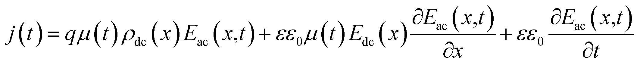
AS is technique based on the measurement of the frequency-dependent capacitance of an organic thin film. For a two-terminal device consisting of an organic semiconductor with a dielectric constant ε and a thickness d, holes are injected from the anode when it is applied a forward dc bias voltage (Vdc). In the case of application of a small ac signal (modulation), with an angular frequency ω = 2πf, the time-dependent injected charge current density j(t) can be given by:30| |
 | (1) |
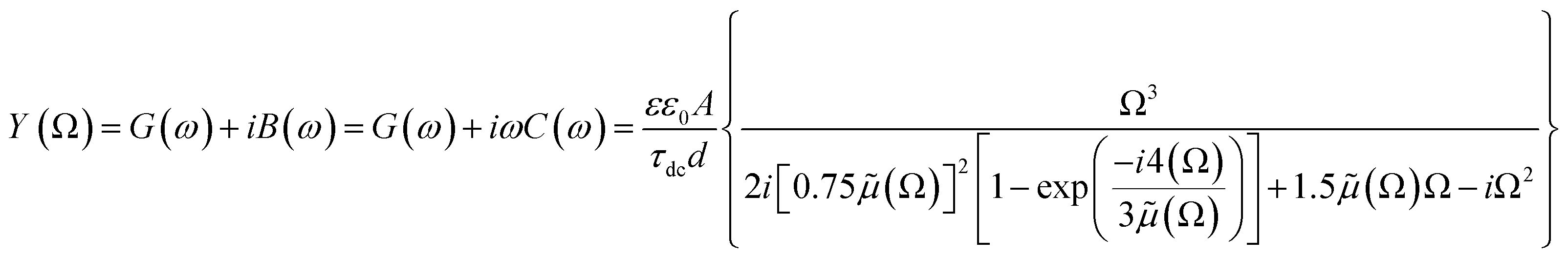
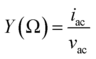
where q is the electron charge, ρdc(x) is the dc charge density, μ(t) is the time dependent mobility, Edc(x) and Eac(x) is the dc and ac electric field components, respectively. According to eqn (1), there are three different contributions to j(t): (1) the response of ρdc(x) in the device. (2) The current due to the additional time-dependent injected charge density. (3) The displacement current by charge relaxation. The complex admittance Y (Ω) is related to iac and vac as follows:  , where G, C and i are the conductance, capacitance and imaginary unit, respectively. It is shown that Y (Ω) can be obtained by applying a Fourier transform to eqn (1):
| |
 | (2) |
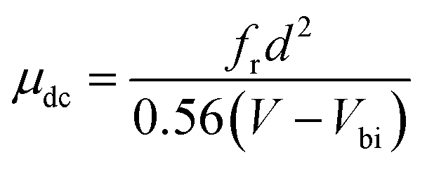
where A and ε0 are the area of the sample and the permittivity of the free space, respectively. In the above equation, τdc is the charge carrier average transit time across the organic thin film in the absence of the ac signal, which is directly related to the energy disorder of organic thin film, and the normalized frequency is defined as Ω = ωτdc. The frequency-dependent capacitance can be re-plotted as the negative differential susceptance −ΔB = −2πf(C − Cgeo), where the geometrical capacitance Cgeo = εε0A/d. The curve typically yields a maximum of −ΔB at a characteristic frequency fr = 0.56/τdc. The carrier mobility can be then extracted by,| |
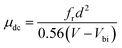 | (3) |
where Vbi is the built-in potential.
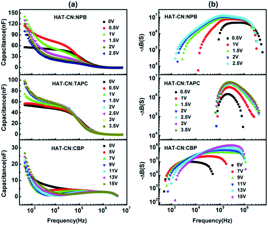
Fig. 3(a) shows C–f curves for the hole-only devices base on HAT-CN:NPB, HAT-CN:TAPC and HAT-CN:CBP mixtures at different applied bias voltages. In the low or intermediate frequency regions, clearly, the capacitances of the three devices decreased with frequency increasing. The reasons are as follows. When the ac-modulation is lower than the characteristic trapping–detrapping time constant, the trap states begin to respond and induce additional capacitive contribution. At further higher frequency, conversely, the trap states cannot follow the ac modulation, the capacitance drops to a plateau, leaving the geometrical capacitance (Cgeo). Toward high frequency, the capacitance becomes little lower than the Cgeo, which is determined by the transit time.31 In the frequency range higher than the fr, the capacitance comes close to the Cgeo because the period of the ac electric field is too short to redistribute the space charges in the mixture devices. As shown in Fig. 3(b), a clear maximum in −ΔB − f occurs at a well defined frequency fr for each device. On the base of eqn (3), the hole mobilities can be calculated, which are summarized in Fig. 4.
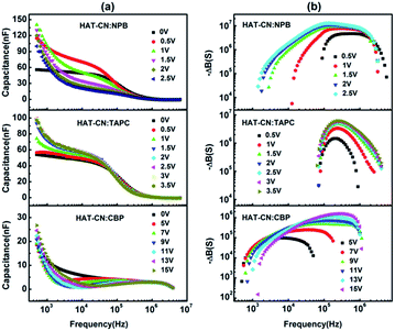 |
| | Fig. 3 (a) Frequency dependence of capacitance of HAT-CN:NPB, HAT-CN:TAPC and HAT-CN:CBP devices at different applied bias voltages. (b) Negative differential susceptance −ΔB dependent frequency of three devices with different applied bias voltages. | |
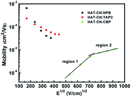 |
| | Fig. 4 Hole mobilities of HAT-CN:NPB, HAT-CN:TAPC and HAT-CN:CBP mixtures against the square root of the electric-field strength. | |
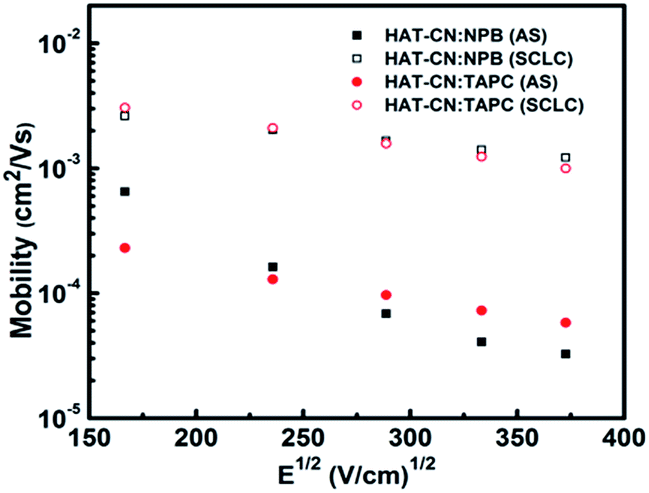
For HAT-CN:NPB and HAT-CN:TAPC mixtures, the mobilities are in the range of 4.1 × 10⁻⁵–6.5 × 10⁻⁴ cm2 V−1 s−1 and 5.8 × 10⁻⁵–2.3 × 10⁻⁴ cm2 V−1 s−1, respectively. As expected from the J–V characteristics of the hole-only devices, HAT-CN:NPB and HAT-CN:TAPC have similar and higher hole mobilities. At the same electric field, the mobility (∼10−4 cm2 V−1 s−1) of the two mixtures calculated by AS measurements is one order of magnitude smaller than our previous result (∼10−3 cm2 V−1 s−1)29 obtained by SCLC technique, as shown in Fig. 5. It may be because the effect of the trap was not considered before. In fact, there exhibits the discrete or shallow trap states in HAT-CN:NPB and HAT-CN:TAPC mixtures according to their C–f characteristics. As we know, the trap states can greatly influence the charge carrier mobility and even the device performance. In addition, the hole mobilities slightly decrease with the electric field increasing, which is in agreement to our previous result.29 The phenomenon of the slightly decreased mobility is considered as to be originated from the presence of certain energetic disorder.32,33 When the descent of the electrostatic potential is comparable and even transcends the energy barrier, for an along-field jump, the dwell time of a carrier on a site approaches the reciprocal rate for that jump because the jump reverse the electric field direction are gradually eliminated. As a result, the transport velocity will saturate with the electric field. Correspondingly, the carrier τdc does not change with the increment of applied voltage. This implies a linear decrease of the carrier mobility because it is controlled by energetically downward jump only that is not accelerated. For HAT-CN:CBP device, however, the hole mobility is in the range of 10−7–10−5 cm2 V−1 s−1. The mobility curve demonstrates two linear parts. (1) In low electric field region, it can be seen that the mobility (8.2 × 10⁻⁷–5.1 × 10⁻⁶ cm2 V−1 s−1) exhibits strong field-dependence and sharply increases as the applied electric field increases. (2) In high electric field region, the mobility (7.4 × 10⁻⁶–1.1 × 10⁻⁵ cm2 V−1 s−1) slightly increases as the electric field increases and almost saturates. This increase should be the trapping effect of trap states. When the electric field increased, the trap depth can be decreased by Poole–Frenkel effect, leading to the increasing mobility. As shown in the inset in Fig. 1, at high applied bias voltage, the J–V curve shows the conductance property of SCLC with exponential traps. This suggests that the hole transport in HAT-CN:CBP mixture is trap-controlled. It is clearly evident that the trapping effect leads to the much lower hole mobility.
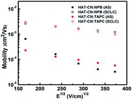 |
| | Fig. 5 Hole mobilities of HAT-CN:NPB and HAT-CN:TAPC mixtures against the square root of the electric-field strength obtained by AS and SCLC techniques, respectively. | |
3.3 Holes transport mechanisms of mixtures
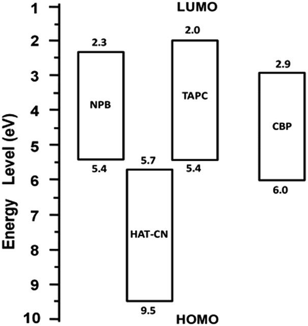
3.3.1 Analysis of energy level. Fig. 6 shows the schematic energy diagram of the four pure semiconductor materials. Energy level values are taken from the literature.34–37 The highest occupied molecular orbital (HOMO) levels of NPB and TAPC are both 5.4 eV, which is only 0.3 eV higher than the lowest unoccupied molecular orbital (LUMO) levels of HAT-CN (5.7 eV). Such energy level distribution can allow the electrons of NPB HOMO or TAPC HOMO to be easily excited to the HAT-CN LUMO, which is sometimes called charge carrier generation. As a consequence, the hole transport abilities of the two mixtures are strong. While the HOMO level of CBP is 6.0 eV, which is 0.3 eV lower than the HAT-CN LUMO. Then the CBP molecule plays the role of traps in the hole transport process, which is also reflected in the J–V characteristics of the HAT-CN:CBP device. The hole mobility of the device is very low due to the influence of traps.
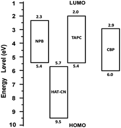 |
| | Fig. 6 Energy level diagram of HAT-CN, NPB, TAPC and CBP. | |
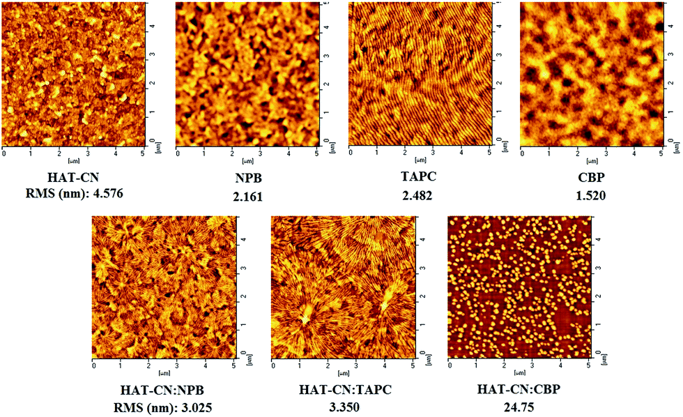
3.3.2 Analysis of AFM. In order to further clarify the holes transport mechanisms in the mixed films, we studied the surface morphologies of the films before and after mixing by AFM. The results are shown in Fig. 7. The root mean square (RMS) of the pure films of HAT-CN, NPB, TAPC and CBP is 4.576 nm, 2.161 nm, 2.482 nm and 1.520 nm, respectively. Clearly, in the four pure films, the RMS of CBP is the smallest. Thus, the RMS of the mixture film of HAT-CN:CBP is as high as 24.75 nm, which is unfavorable for the hole transport. It is further explained the reason of the lowest holes mobility in HAT-CN:CBP device. On the contrary, the RMS of HAT-CN:NPB and HAT-CN:TAPC is 3.025 nm and 3.350 nm, respectively, which is relatively small and close. It is suggested that they have high and similar hole mobilities.
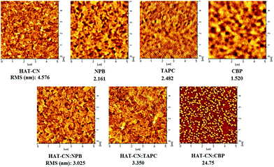 |
| | Fig. 7 The AFM images and roughness of HAT-CN, NPB, TAPC, CBP, HAT-CN:NPB, HAT-CN:TAPC and HAT-CN:CBP films. | |
4 Conclusions
In summary, we have studied the hole transport characteristics and mechanisms of the three small molecule mixtures of HAT-CN:NPB, HAT-CN:TAPC and HAT-CN:CBP. The current–voltage characteristics show that the holes conductions are both SCLC. The hole mobilites of HAT-CN:NPB and HAT-CN:TAPC are determined to be orders of ∼10−4 cm2 V−1 s−1 by AS measurements, which slightly decrease as the electric field increases. Nevertheless, the hole transport in HAT-CN:CBP is SCLC with exponential distribution traps. The hole mobility of HAT-CN:CBP is obtained from 8.2 × 10⁻⁷ to 1.1 × 10⁻⁵ cm2 V−1 s−1, which shows two regions. At low electric field region, the hole mobility (8.2 × 10⁻⁷–5.1 × 10⁻⁶ cm2 V−1 s−1) sharply increases with increasing the electric field. Whereas at high electric field region, the mobility (7.4 × 10⁻⁶–1.1 × 10⁻⁵ cm2 V−1 s−1) slightly increases with increasing the electric field, and almost reaches saturate with the electric field, which should result from the trapping of trap states. Furthermore, the energy level analysis suggests that there are charge carrier generation in HAT-CN:NPB and HAT-CN:TAPC. The CBP molecule acts as a trap during the hole transport process. AFM images clearly show the film surfaces of HAT-CN:NPB and HAT-CN:TAPC mixtures are relatively smooth, which is beneficial to the hole transport. The HAT-CN:CBP film exhibits much rough, indicating the poor hole transport ability. Our results further demonstrate that AS is a simple and powerful tool for the characterization of charge carrier transport properties in organic semiconductor mixtures. We believe that our results will provide critical theoretical information for material selection, device structure design and performance analysis.
Acknowledgements
The authors gratefully acknowledge the National Natural Science Foundation of China (51333007, 91433201, 61204059), Ministry of Science and Technology of China (973 program No. 2013CB834805), the Foundation of Jilin Research Council (2012ZDGG001, 20130206003GX), Chinese Academy of Sciences (KGZD-EW-303-3), Scientific Research Foundation of the Education Department of Shaanxi Province, China (15JK1849) for the support of this research.
References
- G. Yu, J. Gao, J. C. Hummelen and A. J. Heeger, Science, 1995, 270, 1789–1791 CAS.
- L. S. Liao and K. P. Klubek, Appl. Phys. Lett., 2008, 92, 223311 CrossRef.
- W. S. Jeon, J. S. Park, L. Li, D. C. Lim, Y. H. Son, M. C. Suh and J. H. Kwon, Org. Electron., 2012, 13, 939–944 CrossRef CAS.
- Q. X. Guo, H. D. Sun, J. X. Wang, D. Z. Yang, J. S. Chen and D. G. Ma, J. Mater. Chem. C, 2016, 4, 376–382 RSC.
- H. D. Sun, Q. X. Guo, D. Z. Yang, Y. H. Chen, J. S. Chen and D. G. Ma, ACS Photonics, 2015, 2, 271–279 CrossRef CAS.
- L. Burtone, D. Ray, K. Leo and M. Riede, J. Appl. Phys., 2012, 111, 064503 CrossRef.
- N. Gasparini, S. Righi, F. Tinti, A. Savoini, A. Cominetti, R. Po and N. Camaioni, ACS Appl. Mater. Interfaces, 2014, 6, 21416–21425 CAS.
- W. L. Ma, C. Y. Yang, X. Gong, K. Lee and A. J. Heeger, Adv. Funct. Mater., 2005, 15, 1617–1622 CrossRef CAS.
- M. Redecker, D. D. C. Bradley, M. Inbasekaran and E. P. Woo, Appl. Phys. Lett., 1998, 73, 1565 CrossRef CAS.
- A. J. Campbell, D. D. C. Bradley and H. Antoniadis, J. Appl. Phys., 2001, 89, 3343 CrossRef CAS.
- P. W. M. Blom and M. C. J. M. Vissenberg, Phys. Rev. Lett., 1998, 80, 3819 CrossRef CAS.
- S. C. Tse, H. H. Fong and S. K. So, J. Appl. Phys., 2003, 94, 2033 CrossRef CAS.
- D. Poplavskyy, J. Nelson and D. D. C. Bradley, Appl. Phys. Lett., 2003, 83, 707 CrossRef CAS.
- N. L. Hong, X. Q. Qiu, W. Y. Deng, Z. C. He and Y. Li, RSC Adv., 2015, 5, 90913–90921 RSC.
- P. Anjaneyulu, C. S. Suchand Sangeeth and R. Menon, J. Appl. Phys., 2010, 107, 093716 CrossRef.
- M. Hoping, C. Schildknecht, H. Gargouri, T. Riedl, M. Tilgner, H. H. Johannes and W. Kowalsky, Appl. Phys. Lett., 2008, 92, 213306 CrossRef.
- S. Bellani, A. Iacchetti, M. Porro, L. Beverina, M. R. Antognazza and D. Natali, Org. Electron., 2015, 22, 56–61 CrossRef CAS.
- S. Ishihara, H. Hase, T. Okachi and H. Naito, Org. Electron., 2011, 12, 1364–1369 CrossRef CAS.
- S. W. Tsang, S. C. Tse, K. L. Tong and S. K. So, Org. Electron., 2006, 7, 474–479 CrossRef CAS.
- E. Ehrenfreund, C. Lungenschmied, G. Dennler, H. Neugebauer and N. S. Sariciftci, Appl. Phys. Lett., 2007, 91, 012112 CrossRef.
- K. H. Chan and S. K. So, J. Photonics Energy, 2011, 1, 011011 CrossRef.
- J. You, L. Dou, K. Yoshimura, T. Kato, K. Ohya, T. Moriarty, K. Emery, C. C. Chen, J. Gao, G. Li and Y. Yang, Nat. Commun., 2013, 4, 1446 CrossRef PubMed.
- Y.-K. Kim, K. J. Won and Y. Park, Appl. Phys. Lett., 2009, 94, 063305 CrossRef.
- P. S. Szalay, J. R. Galan-Mascaros, B. L. Schottel, J. Bacsa, L. M. Perez, A. S. Ichimura, A. Chouai and K. R. Dunbar, J. Cluster Sci., 2004, 15, 503–530 CrossRef CAS.
- P. Frank, N. Koch, M. Koini, R. Rieger, K. Müllen, R. Resel and A. Winkler, Chem. Phys. Lett., 2009, 473, 321 CrossRef CAS.
- H. Glowatzki, B. Broker, R. P. Blum, O. T. Hofmann, A. Vollmer, R. Rieger, K. Mullen, E. Zojer, J. P. Rabe and N. Koch, Nano Lett., 2008, 8, 3825–3829 CrossRef CAS PubMed.
- L. S. Liao and K. P. Klubek, Appl. Phys. Lett., 2008, 92, 223311 CrossRef.
- D. H. Kim and T. W. Kim, Org. Electron., 2014, 15, 3452–3457 CrossRef CAS.
- Y. P. Wang, J. Y. Huang, J. S. Chen, X. F. Qiao, D. Z. Yang, D. G. Ma and L. S. Dong, Chin. Phys. Lett., 2016, 33, 027302 CrossRef.
- S. W. Tsang, S. K. So and J. B. Xu, J. Appl. Phys., 2006, 99, 013706 CrossRef.
- J. Shao and G. T. Wright, Solid-State Electron., 1961, 3, 291–303 CrossRef.
- A. J. Mozer, N. S. Sariciftci, A. Pivrikas, R. Österbacka, G. Juška, L. Brassat and H. Bässler, Phys. Rev. B: Condens. Matter Mater. Phys., 2005, 71, 035214 CrossRef.
- K. Seki and M. Tachiya, Phys. Rev. B: Condens. Matter Mater. Phys., 2001, 65, 014305 CrossRef.
- K. S. Yook, S. O. Jeon and J. Y. Lee, Thin Solid Films, 2009, 517, 6109–6111 CrossRef CAS.
- K. Goushi, R. Kwong, J. J. Brown, H. Sasabe and C. Adachi, J. Appl. Phys., 2004, 95, 7798 CrossRef CAS.
- J. Wünsche, S. Reineke, B. Lüssem and K. Leo, Phys. Rev. B: Condens. Matter Mater. Phys., 2010, 81, 245201 CrossRef.
- M. E. Kondakova, T. D. Pawlik, R. H. Young, D. J. Giesen, D. Y. Kondakov, C. T. Brown, J. C. Deaton, J. R. Lenhard and K. P. Klubek, J. Appl. Phys., 2008, 104, 094501 CrossRef.
|
| This journal is © The Royal Society of Chemistry 2017 |
Click here to see how this site uses Cookies. View our privacy policy here. 
 Open Access Article
 This Open Access Article is licensed under a
  *a,
Qingcheng Lianga,
Jinying Huangb,
Dongge Ma
*a,
Qingcheng Lianga,
Jinying Huangb,
Dongge Ma
 , where G, C and i are the conductance, capacitance and imaginary unit, respectively. It is shown that Y (Ω) can be obtained by applying a Fourier transform to eqn (1):