
 Open Access Article
 This Open Access Article is licensed under a Creative Commons Attribution-Non Commercial 3.0 Unported Licence
Chemical vapor deposition of partially oxidized graphene
Zafer Mutlu†
a,
Isaac Ruiz†b,
Ryan J. Wu c,
Robert Ionescua,
Sina Shahrezaeia,
Selcuk Temiza,
Mihrimah Ozkanb,
K. Andre Mkhoyanc and
Cengiz S. Ozkan*ad
c,
Robert Ionescua,
Sina Shahrezaeia,
Selcuk Temiza,
Mihrimah Ozkanb,
K. Andre Mkhoyanc and
Cengiz S. Ozkan*ad
aMaterials Science and Engineering Program, University of California, Riverside, CA 92521, USA. E-mail: cozkan@engr.ucr.edu
bDepartment of Electrical and Computer Engineering, University of California, Riverside, CA 92521, USA
cDepartment of Chemical Engineering and Materials Science, University of Minnesota, Minneapolis, MN 55455, USA
dDepartment of Mechanical Engineering, University of California, Riverside, CA 92521, USA
First published on 23rd June 2017
Abstract
Herein, we report on chemical vapor deposition (CVD) of partially oxidized graphene (POG) films on electropolished polycrystalline copper foils at relatively low temperature under near-atmospheric pressure. The structural, chemical, and electronic properties of the films are studied in detail using several spectroscopic and microscopic techniques. The content of carbon and oxygen in the films is identified by chemical mapping at near-atomic scale. Electron diffraction patterns of the films possess clear diffraction spots with a six-fold pattern that is consistent with the hexagonal lattice. The fine structure of the carbon K-edge signal in STEM-EELS spectra of the films is distinguishable from that of graphene and graphite. The presence of oxygen in the films is further supported by a clear oxygen K-edge. Raman spectroscopy and XPS results provide direct evidence for a lower degree of oxidation. The work function of the films is found to be much higher than that of graphene, using UPS measurements.
Introduction
Graphene oxide (GO), a heavily oxidized derivative of graphene, has recently gained extraordinary attention for its great potential use as an intermediate in the mass production of graphene,1 and a broad range of applications.1,2 GO can be visualized as individual sheets of graphene decorated with oxygen functional groups on both basal planes and edges.3GO can be synthesized by various methods, as reported by Staudenmaier,4 Hofmann,5 Hummers,6 and Tour,7 where bulk graphite is generally chemically oxidized to graphite oxide and then exfoliated to the individual layers of GO. Among these methods, Hummers' method is the most common method used today for mass production of graphene. In Hummers' method, the oxidation of graphite is accomplished by treating graphite with potassium permanganate (KMnO4) and sodium nitrate (NaNO3) in concentrated sulfuric acid (H2SO4). The common challenges associated with these GO production routes include chemical inhomogeneity, batch-to-batch reproducibility and generation of defects.8 The surface properties, structural features, purity, and colloidal dispersity of GO vary substantially depending on the synthesis method used due to the differences in the reaction conditions, type of graphitic material and purification processing used.9
Band gap opening and scaling is one of the priorities in the development of graphene-based electronics. GO is an insulator,10 but controlled removal of oxygen functional groups can transform it to a semiconductor and ultimately to a semi-metal graphene.11 On the other hand, it is possible to open a band gap in graphene by adding oxygen functional groups onto its surface by plasma treatment.12,13 Ideally, by controlling the oxidation degree, one can engineer the band gap of graphene. However, oxygen plasma treatment can introduce structural disorders and defects into graphene layers, and suffers from non-uniform functionalization, and additional processing steps, which hinders its potential applications.
Chemical vapor deposition (CVD) has emerged as the most versatile and promising technique to grow graphene14 and graphene-like 2D materials.15–18 However, the formation of graphene nucleation with high density on copper (Cu) foils at the initial stage of CVD growth can lead to high-density domain boundaries in graphene films, resulting in severe degradation of its carrier transport properties19 and mechanical strength.20 Recently, several research groups21–25 have reported that treating the surface of Cu foils with oxygen can significantly reduce graphene nucleation density, resulting large graphene domains. While most of the previous research26 has focused on improving graphene growth using oxygen, less attention27,28 has been paid to CVD growth of GO and its derivatives using oxygen.
Herein, we have demonstrated CVD growth of partially oxidized graphene (POG) films on electropolished polycrystalline Cu foils, treated with a gas mixture containing oxygen and hydrogen just before graphene growth, at relatively low temperature under near-atmospheric pressure. Our method is significantly different than the previously published work27 in terms of the growth technique, experimental conditions including underlying substrate, temperature, and pressure, and overall material quality. We have performed CVD of POG films at a growth temperature of 800 °C, which is relatively lower than those for reported graphene (1000 °C)14 and slightly oxidized graphene growths (1100 °C).27 Detailed characterization of the films is performed using various microscopy and spectroscopy methods. We also provide a discussion concerning comparison of our results with other results obtained in the literature for GO and its derivatives.
Methods
Materials synthesis
Materials characterization
Results and discussion
As described in Methods, we grew a POG film on an electropolished polycrystalline Cu foil at relatively low temperature under near-atmospheric pressure via CVD with help of oxygen. We then transferred the film (∼1 cm × 1 cm) onto a SiO2/Si substrate via the electrochemical delamination method (see Methods for details), as seen in Fig. 1a, and checked under optical microscopy and AFM.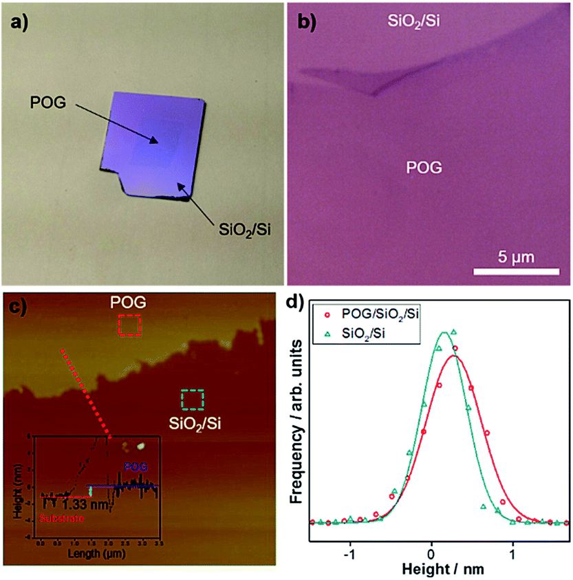 | ||
| Fig. 1 Surface morphology of POG films. Digital photo (a) and optical microscopy (b) image of a CVD-grown POG film (∼1 cm × 1 cm) transferred onto a SiO2/Si substrate via electrochemical delamination method. (c) High resolution AFM topography image of a boundary between the POG film and the SiO2/Si substrate. Inset shows the height profile along the dashed lines. (d) Comparison of the height histograms for the POG film on the SiO2/Si substrate (open red circles) and the SiO2/Si substrate (open dark cyan triangles). The data, corresponding to the regions designated by the dashed red and dark cyan squares (200 nm × 200 nm) in (c), are described by Gaussian distributions (solid lines) with standard deviations σ of 0.33 nm, and 0.27 nm, respectively. The height data was obtained by subtracting the mean value of the raw data, which allows the peak to be aligned in the middle. | ||
Fig. 1b represents the optical microscopy image of the POG film on the SiO2/Si substrate. The POG film with contrast is visible and can be easily distinguished from the substrate, similar to the case of GO,30 graphene31 and other 2D materials17,32 on SiO2/Si, due to the interference effects.33–35 It appears that the POG film has a flat, smooth, transparent, and sheet-like surface with no observable pits or defects, except that the deformations including folds and wrinkles are formed at its edge possibly during the transfer process.
AFM in non-contact mode was employed to measure the thickness of the POG film. A typical high-resolution AFM topographic image acquired for region surrounding the edge of the POG film on the SiO2/Si substrate is shown in Fig. 1c. Inset shows the height profile along the dashed lines. The height profile clearly shows that the edge of the film has a thickness of 1.33 nm, which is close to the thickness of monolayer GO reported by Mkhoyan et al.10 The large edge step in the height profile can be attributed to the PMMA reside introduced during the transfer process since the dangling bonds at the edges of POG films are attractive to the PMMA molecules, which are difficult to remove by acetone and IPA.
We also examined the surface roughness of the POG film and compared it with the underlying SiO2/Si substrate by constructing the height histograms and calculating the standard deviations σ of these distributions from the high-resolution AFM topographic image in Fig. 1c. These histograms could be fit well by single Gaussian functions.36,37 Fig. 1d compares the corresponding height histograms for the POG film and SiO2/Si substrate surfaces, which are measured in squares (200 nm × 200 nm) in Fig. 1c. The histograms are described by Gaussian distributions with the standard deviations σ 0.33 nm and 0.27 nm, respectively, for the POG film on the SiO2/Si substrate, and the bare SiO2/Si substrate. Both curves are almost similar to each other, indicating that the POG film surface largely follows the underlying substrate morphology. The carbon-oxygen bonds and oxygen bonds alone can be also responsible for the surface roughness of the POG film.10 The surface roughness of the POG film on the SiO2/Si substrate is comparable to that of GO on a SiO2/Si substrate.10
To check for the chemical composition, we transferred POG films onto a holey carbon TEM grid via an electrochemical delamination method, as described in Methods, and characterized with high angle annular dark-field (HAADF)-STEM imaging and energy-dispersive X-ray spectroscopy (EDX) mappings. These measurements provide information on the elemental distribution at the atomic scale.38 Fig. 2a shows an HAADF-STEM image of a POG film suspended over a hole (∼1 μm) of the TEM grid. It is likely that the POG film was folded during the transfer onto the grid.39 The small particles of high intensity (bright white) dispersed throughout the film are copper-oxide particles as determined by EDX elemental mapping in Fig. 2b. The copper-oxide particles over the film were most likely formed during the growth.14 The Cu signal outside of the particles are mainly secondary signals originating from the Cu grid bars holding the TEM grid together. The presence of carbon and oxygen in the POG film was confirmed by STEM-EDX elemental mappings in Fig. 2c and d, respectively.
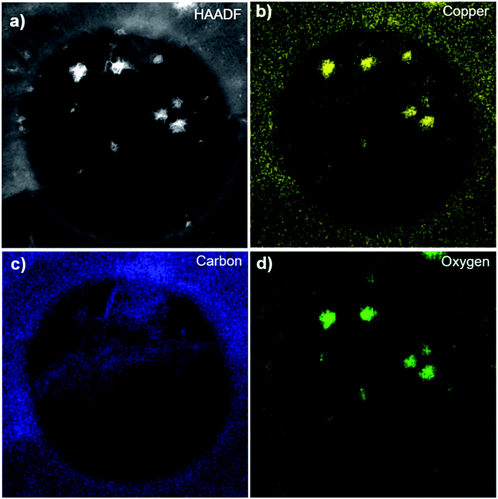 | ||
| Fig. 2 Chemical composition of POG films. HAADF-STEM image (a) and corresponding Cu (b), carbon (c) and oxygen (d) elemental mappings of the POG film suspended over a holey carbon TEM grid collected using STEM-EDX. The diameter of the hole of the grid is ∼1 μm. | ||
We studied the atomic and electronic structure of POG films using ADF-STEM imaging and EELS for measuring the fine structure of carbon and oxygen K-edges in a STEM. Fig. 3a shows a low magnification ADF-STEM image of a POG film. We collected SAED patterns in two different regions on the ADF image. Fig. 3b contains a SAED pattern collected from a monolayer region of the POG film. The SAED pattern shows that the structure of the film is hexagonal with a basal plane lattice parameter of a = 2.45 ± 0.05 Å which is characteristic of graphene40 and GO.41 This hexagonal structure is also evident in Fig. 3c, which contains a SAED pattern collected from a region of two overlapping POG monolayer films. The overlap creates two sets of hexagonal diffraction spots in the SAED pattern that are rotated by an amount equivalent to the actual offset of the POG films, which, in this case, is about 20%.
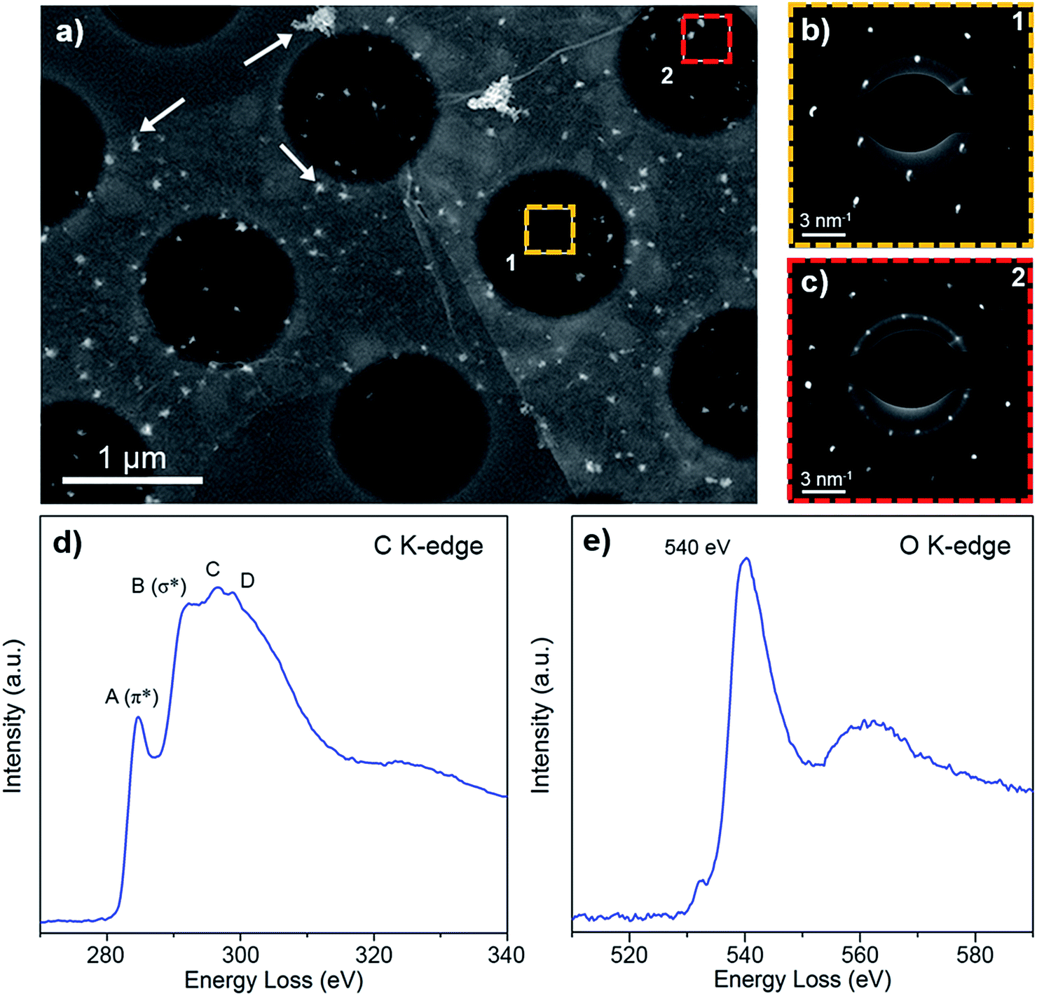 | ||
| Fig. 3 Atomic and electronic structure of POG films. Low magnification ADF-STEM image (a) of a POG film on a holey carbon TEM grid. Arrows indicate copper-oxide particles detected on the POG film. SAED pattern from a single (b) and two overlapping (c) POG films. The locations of SAED pattern acquisition are indicated by square boxes in panel (a). EELS spectra of the C K-edge (d) showing signature GO fine structure, and the O K-edge (e). | ||
In order to distinguish the POG film from graphene or graphite, EELS data of carbon and oxygen K-edge were collected as shown in Fig. 3d and e, respectively. The energies and relative intensities of the peaks in the fine structure of carbon (C) K-edge (features A to D) are consistent with previous EELS measurements of GO reported in literature.10 This fine structure is unique to GO and is distinguishable from that of graphene and graphite.10 The presence of oxygen in the films is further supported by a clear oxygen (O) K-edge EELS signal. Its peak onset at 530 eV and its maximum at 540 eV are consistent to a previous report.10 It is worth mentioning that we also detected graphene and graphite regions in the POG film during STEM-EELS measurements.
Raman spectroscopy has proven to be highly useful as a non-invasive technique in the structural characterization of graphene and its derivatives.42–45 Herein, we used Raman spectroscopy to identify POG films using a 532 nm excitation laser. The excitation power was kept at 2 mW to avoid local heating. Fig. 4a represents the optical microcopy image of a POG film, where Raman spectra was collected. The Raman spectra of the POG film consist of prominent D and G peaks, and weak 2D and D + G peaks in Fig. 4b. These features are similar to those seen GO1,7,46 and its derivatives,47–49 but deviate from those of graphene, where the D peak is absent or small, and the other peaks are more clearly defined.44,50 The G peak at around 1616 cm−1 is due to the bond stretching of all pairs of sp2 atoms in both rings and chains.44,51–53 The D peak at around 1355 cm−1 is due to the breathing modes of sp2 atoms in rings,44,52,54 which originates from the structural imperfections created by the attachment of oxygen functional groups on carbon atoms.55 Generally, the intensity ratio of the D and G peaks (ID/IG) indicates the degree of disorder and oxygenation in a sp3/sp2 hybrid network of carbon atoms.56–60 We calculated an ID/IG ratio of ∼1.06 for the POG film, which is comparable to that of the POG sheets reported by Goki Eda et al.48 The size of the defect-free sp2 carbon clusters, La,53,54 was estimated to be ∼9.8 nm for the POG film, which is greater than that of GO reported in the literature,48,61 consistent with the low oxygen content and low defect density. The overtone of the D peak, called 2D peak, appears around 2688 cm−1 is due to double resonance transitions resulting in production of two phonons with opposite momentum.44 The low intensity and broad shape of the 2D peak is attributed to breaking of stacking order associated with oxidation reaction.62,63 The disorder-induced combination mode of G and D bands,64–66 called D + G peak (also known as D + D′ peak), appears around 2942 cm−1. The intensity ratio of the 2D and D + G peaks (I2D/ID+G) can be associated with defect density and oxygen content in GO and its derivatives.58,62 This ratio is relatively low in the POG film, compare to that of GO,48 indicating the low defect concentration in the POG film accompanied by a lower oxygen content.58,62 We obtained Raman spectra for different spots of the POG film, and did not see a significant difference in the spectra. We also examined the effect of the folding on the Raman spectra of the POG film. The Raman spectra of the unfolded and folded parts of the POG film are represented in Fig. 4a, both of which was measured under the same experimental conditions. It is observed from the Raman spectra that folding gives rise to a significant increase in the intensities of the Raman peaks, suggesting that Raman signal is proportional to thickness of the film. In addition, no obvious shift position shift is observed in the Raman bands.
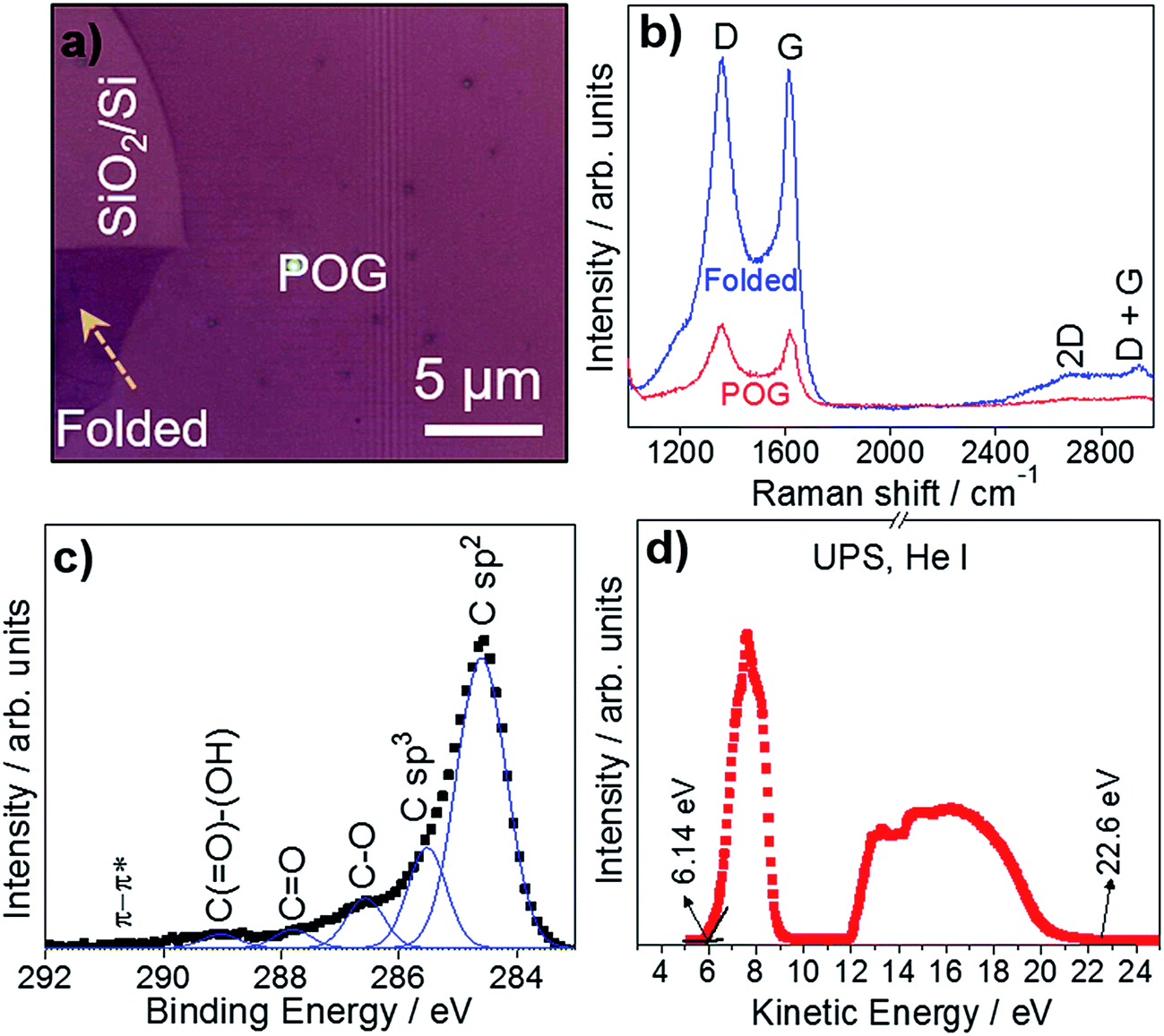 | ||
| Fig. 4 Chemical and electronic properties of POG films. (a) The optical microscopy image of a POG film where Raman spectra were collected. (b) Raman spectra collected from the non-folded and folded regions of the POG film. (b and c) The C 1s region of the XPS spectra for the POG film. The spectra were deconvoluted to 6 components as described in the text. (d) Work functions of the POG film determined by UPS measurements with He I (hν = 21.2 eV) source. | ||
XPS, a surface sensitive technique, provides information on the surface chemistry of materials being analyzed.18,67 XPS revealed the nature of the carbon bonds present in POG films. Fig. 4c shows the C 1s region of the XPS spectra for the POG film. After a Shirley background subtraction,68 the high-resolution C 1s peak region of the XPS spectra was deconvoluted to the components, which are expected to be present in the film,48,69,70 using Gaussian function. The deconvoluted C 1s peak region mainly consists of C sp2, C sp3, C–O, C![[double bond, length as m-dash]](https://www.rsc.org/images/entities/char_e001.gif) O, C(O)–(OH) and π–π* at 284.60, 285.52, 286.57, 287.80, 289.03, and 290.72 eV, respectively, which consistent with the literature.48,58,71 The majority of carbon atoms in the POG film has the sp2 hybridization, originating from unoxidized carbon atoms.49 The weaker sp3 hybridization of carbon atoms is due to the formation of covalent bonds during the oxidation.49 The peak intensity ratio of oxygenated carbon peaks and non-oxygenated carbon peaks reflects the oxidation degree of the films.59,72,73 In contrast to GO,11,48 the peak intensity of oxygenated groups of the POG film is much weaker than that of non-oxygenated carbon peaks, suggesting that the POG is partially oxidized,58,74 which is in good agreement with our Raman results. For the POG film, we found the oxygen content to be ∼4.3%.
O, C(O)–(OH) and π–π* at 284.60, 285.52, 286.57, 287.80, 289.03, and 290.72 eV, respectively, which consistent with the literature.48,58,71 The majority of carbon atoms in the POG film has the sp2 hybridization, originating from unoxidized carbon atoms.49 The weaker sp3 hybridization of carbon atoms is due to the formation of covalent bonds during the oxidation.49 The peak intensity ratio of oxygenated carbon peaks and non-oxygenated carbon peaks reflects the oxidation degree of the films.59,72,73 In contrast to GO,11,48 the peak intensity of oxygenated groups of the POG film is much weaker than that of non-oxygenated carbon peaks, suggesting that the POG is partially oxidized,58,74 which is in good agreement with our Raman results. For the POG film, we found the oxygen content to be ∼4.3%.
We also calculated the work function of POG films by UPS using excitation energy of 21.20 eV. Fig. 4d exhibits the UPS spectra of the POG film. From the UPS spectra, the work function was estimated as the energy level difference between the inelastic cutoff and the Fermi edge.75 The calculated work function of the POG film is Φ = 4.74 eV, which is comparable to that of reduced graphene oxide (rGO),75,76 but much higher than that of graphene.77
Conclusions
We have demonstrated a CVD method to grow POG films under near atmospheric pressure at reduced temperatures. The work reported here can be considered as a first step to growing the oxidized graphene films by CVD. We comprehensively characterize the films to establish unambiguously the fundamental properties using several spectroscopy and microscopy methods. The presence of oxygen with low concentration in the graphene films was confirmed by spectroscopic characterization. The atomic and electronic structure of the POG films was revealed by STEM-EELS analysis. Our results offer a promising route towards the growth of oxidized graphene films with controllable oxygen concentration, which could be useful in various types of basic and applied research on GO based materials.Acknowledgements
This work was supported by the STARnet Center C-SPIN (Center for Spintronic Materials, Interfaces and Novel Architectures), through the Semiconductor Research Corporation sponsored by the MARCO (Microelectronics Advanced Research Corporation) and the DARPA (Defense Advanced Research Projects Agency). X-ray photoelectron spectroscopy (XPS) and ultraviolet photoelectron spectroscopy (UPS) measurements were performed in the Analytical Chemistry Instrumentation Facility (ACIF) of University of California, Riverside, which receives support from NSF (National Science Foundation) through MRI (Major Research Instrumentation) program (DMR-0958796). Scanning transmission electron microscopy (STEM) and electron energy loss spectroscopy (EELS) analysis were performed in the Characterization Facility of University of Minnesota, which receives partial support from NSF through MRSEC (Materials Research Science and Engineering Centers) program (DMR-1420013).References
- Y. Zhu, S. Murali, W. Cai, X. Li, J. W. Suk, J. R. Potts and R. S. Ruoff, Adv. Mater., 2010, 22, 3906 CrossRef CAS PubMed.
- D. R. Dreyer, A. D. Todd and C. W. Bielawski, Chem. Soc. Rev., 2014, 43, 5288 RSC.
- A. Ganguly, S. Sharma, P. Papakonstantinou and J. Hamilton, J. Phys. Chem. C, 2011, 115, 17009 CAS.
- L. Staudenmaier, Ber. Dtsch. Chem. Ges., 1898, 31, 1481 CrossRef CAS.
- U. Hofmann and R. Holst, Ber. Dtsch. Chem. Ges., 1939, 72, 754 CrossRef.
- W. S. Hummers and R. E. Offeman, J. Am. Chem. Soc., 1958, 80, 1339 CrossRef CAS.
- D. C. Marcano, D. V. Kosynkin, J. M. Berlin, A. Sinitskii, Z. Sun, A. Slesarev, L. B. Alemany, W. Lu and J. M. Tour, ACS Nano, 2010, 4, 4806 CrossRef CAS PubMed.
- Y. L. Zhong, Z. Tian, G. P. Simon and D. Li, Mater. Today, 2015, 18, 73 CrossRef CAS.
- A. J. Dhifaf, L. Neus and K. Kostas, 2D Mater., 2016, 3, 14006 CrossRef.
- K. A. Mkhoyan, A. W. Contryman, J. Silcox, D. A. Stewart, G. Ed, C. Mattevi, S. Miller and M. Chhowalla, Nano Lett., 2009, 9, 1058 CrossRef CAS PubMed.
- D. R. Dreyer, S. Park, C. W. Bielawski and R. S. Ruoff, Chem. Soc. Rev., 2010, 39, 228 RSC.
- A. Nourbakhsh, M. Cantoro, T. Vosch, G. Pourtois, F. Clemente, M. H. V. D. Veen, J. Hofkens, M. M. Heyns, S. D. Gendt and B. F. Sels, Nanotechnology, 2010, 21, 435203 CrossRef PubMed.
- T. Gokus, R. R. Nair, A. Bonetti, M. Böhmler, A. Lombardo, K. S. Novoselov, A. K. Geim, A. C. Ferrari and A. Hartschuh, ACS Nano, 2009, 3, 3963 CrossRef CAS PubMed.
- I. Ruiz, W. Wang, A. George, C. S. Ozkan and M. Ozkan, Adv. Sci., Eng. Med., 2014, 6, 1070 CrossRef CAS.
- Z. Mutlu, R. J. Wu, D. Wickramaratne, S. Shahrezaei, C. Liu, S. Temiz, A. Patalano, M. Ozkan, R. K. Lake, K. A. Mkhoyan and C. S. Ozkan, Small, 2016, 12, 2998 CrossRef CAS PubMed.
- Z. Mutlu, D. Wickramaratne, S. Turkyilmaz, H. H. Bay, Z. Favors, M. Ozkan, R. Lake and C. Ozkan, J. Nanosci. Nanotechnol., 2017, 16, 8419 CrossRef.
- Z. Mutlu, M. Ozkan and C. S. Ozkan, Mater. Chem. Phys., 2016, 176, 52 CrossRef CAS.
- Z. Mutlu, S. Shahrezaei, S. Temiz, M. Ozkan and C. S. Ozkan, J. Electron. Mater., 2016, 45, 2115 CrossRef CAS.
- O. V. Yazyev and S. G. Louie, Nat. Mater., 2010, 9, 806 CrossRef CAS PubMed.
- C. S. R. Vargas, H. L. Zhuang, P. Y. Huang, A. M. V. D. Zande, S. Garg, P. L. Mceuen, D. A. Muller, R. G. Hennig and J. Park, Nano Lett., 2011, 11, 2259 CrossRef PubMed.
- Y. Hao, M. S. Bharathi, L. Wang, Y. Liu, H. Chen, S. Nie, X. Wang, H. Chou, C. Tan, B. Fallahazad, H. Ramanarayan, C. W. Magnuson, E. Tutuc, B. I. Yakobson, K. F. McCarty, Y. W. Zhang, P. Kim, J. Hone, L. Colombo and R. S. Ruoff, Science, 2013, 342, 720 CrossRef CAS PubMed.
- C. W. Magnuson, X. Kong, H. Ji, C. Tan, H. Li, R. Piner, C. A. Ventrice and R. S. Ruoff, J. Mater. Res., 2014, 29, 403 CrossRef CAS.
- Z. R. Robinson, E. W. Ong, T. R. Mowll, P. Tyagi, D. K. Gaskill, H. Geisler and C. A. Ventrice, J. Phys. Chem. C, 2013, 117, 23919 CAS.
- P. B. Weimer, B. Brennan, A. J. Pollard and S. Hofmann, Chem. Mater., 2016, 28, 8905 CrossRef PubMed.
- R. J. Chang, C. H. Lee, M. K. Li, C. W. Chen and C. Y. Wen, Nanoscale, 2017, 9, 2324–2329 RSC.
- T. Liang, C. Luan, H. Chen and M. Xu, Nanoscale, 2017, 9, 3719–3735 RSC.
- R. U. R. Sagar, M. Namvari, S. T. Navale and F. J. Stadler, J. Colloid Interface Sci., 2017, 490, 844–849 CrossRef CAS PubMed.
- Y. Liu and Y. Chen, J. Appl. Phys., 2016, 119, 1–7 Search PubMed.
- Y. Wang, Y. Zheng, X. Xu, E. Dubuisson, Q. Bao, J. Lu and K. P. Loh, ACS Nano, 2011, 5, 9927–9933 CrossRef CAS PubMed.
- I. Jung, J. S. Rhyee, J. Y. Son, R. S. Ruoff and K. Y. Rhee, Nanotechnology, 2012, 23, 25708 CrossRef PubMed.
- S. P. Koenig, N. G. Boddeti, M. L. Dunn and J. S. Bunch, Nat. Nanotechnol., 2011, 6, 543–546 CrossRef CAS PubMed.
- R. Ionescu, W. Wang, Y. Chai, Z. Mutlu, I. Ruiz, Z. Favors, D. Wickramaratne, M. Neupane, L. Zavala, R. Lake, M. Ozkan and C. S. Ozkan, IEEE Trans. Nanotechnol., 2014, 13, 749–754 CrossRef CAS.
- S. Roddaro, P. Pingue, V. Piazza, V. Pellegrini and F. Beltram, Nano Lett., 2007, 7, 2707–2710 CrossRef CAS PubMed.
- P. Blake, E. W. Hill, A. H. C. Neto, K. S. Novoselov, D. Jiang, R. Yang, T. J. Booth and A. K. Gei, Appl. Phys. Lett., 2007, 91, 063124 CrossRef.
- A. Reina, X. Jia, J. Ho, D. Nezich, H. Son, V. Bulovic, M. S. Dresselhaus and J. Kong, Nano Lett., 2009, 9, 30–35 CrossRef CAS PubMed.
- S. Hwang, H. Seo, D. C. Jeong, L. Wen, J. G. Han, C. Song and Y. Kim, Sci. Rep., 2015, 5, 11201 CrossRef PubMed.
- C. H. Lui, L. Liu, K. F. Mak, G. W. Flynn and T. F. Heinz, Nature, 2009, 462, 339–341 CrossRef CAS PubMed.
- J. S. Jeong, M. L. Odlyzko, P. Xu, B. Jalan and K. A. Mkhoyan, Phys. Rev. B, 2016, 93, 165140 CrossRef.
- J. R. Kyle, C. S. Ozkan and M. Ozkan, Nanoscale, 2012, 4, 3807–3819 RSC.
- J. C. Meyer, A. K. Geim, M. I. Katsnelson, K. S. Novoselov, T. J. Booth and S. Roth, Nature, 2007, 446, 60–63 CrossRef CAS PubMed.
- N. R. Wilson, P. A. Pandey, R. Beanland, R. J. Young, I. A. Kinloch, L. Gong, Z. Liu, K. Suenaga, J. P. Rourke, S. J. York and J. Sloan, ACS Nano, 2009, 3, 2547–2556 CrossRef CAS PubMed.
- A. C. Ferrari, J. C. Meyer, V. Scardaci, C. Casiraghi, M. Lazzeri, F. Mauri, S. Piscanec, D. Jiang, K. S. Novoselov, S. Roth and A. K. Geim, Phys. Rev. Lett., 2016, 97, 187401 CrossRef PubMed.
- A. C. Ferrari and D. M. Basko, Nat. Nanotechnol., 2013, 8, 235–246 CrossRef CAS PubMed.
- A. C. Ferrari, Solid State Commun., 2007, 143, 47–57 CrossRef CAS.
- C. Liu, C. Li, K. Ahmed, Z. Mutlu, C. S. Ozkan and M. Ozkan, Sci. Rep., 2016, 6, 29183 CrossRef CAS PubMed.
- K. N. Kudin, B. Ozbas, H. C. Schniepp, R. K. Prud'homme, I. A. Aksay and R. Car, Nano Lett., 2008, 8, 36–41 CrossRef CAS PubMed.
- I. K. Moon, J. Lee, R. S. Ruoff and H. Lee, Nat. Commun., 2010, 1, 73 Search PubMed.
- G. Eda, J. Ball, C. Mattevi, M. Acik, L. Artiglia, G. Granozzi, Y. Chabal, T. D. Anthopoulos and M. Chhowalla, J. Mater. Chem., 2011, 21, 11217 RSC.
- S. Abdolhosseinzadeh, H. Asgharzadeh and H. Seop Kim, Sci. Rep., 2015, 5, 10160 CrossRef CAS PubMed.
- J. K. Reiber, A. Guvenc, W. Wang, M. Ghazinejad, J. Lin, S. Guo, C. S. Ozkan and M. Ozkan, Small, 2011, 7, 2599–2606 CrossRef PubMed.
- A. C. Ferrari and J. Robertson, Phys. Rev. B: Condens. Matter Mater. Phys., 2001, 64, 75414 CrossRef.
- L. M. Malard, M. A. Pimenta, G. Dresselhaus and M. S. Dresselhaus, Phys. Rep., 2009, 473, 51–87 CrossRef CAS.
- I. Childres, L. Jauregui, W. Park, H. Cao and Y. Chen, New Dev. Photon Mater. Res., 2013, 1–20 Search PubMed.
- L. G. Cançado, A. Jorio, E. H. Ferreira, F. Stavale, C. A. Achete, R. B. Capaz, M. V. O. Moutinho, A. Lombardo, T. Kulmala and A. C. Ferrari, Nano Lett., 2011, 11, 3190–3196 CrossRef PubMed.
- D. Chen, H. Feng and J. Li, Chem. Rev., 2012, 112, 6027–6053 CrossRef CAS PubMed.
- S. Eigler, C. Dotzer and A. Hirsch, Carbon, 2012, 50, 3666–3673 CrossRef CAS.
- S. Pei and H. M. Cheng, Carbon, 2012, 50, 3210–3228 CrossRef CAS.
- Y. Xu, K. Sheng, C. Li and G. Shi, J. Mater. Chem., 2011, 21, 7376 RSC.
- G. Sobon, J. Sotor, J. Jagiello, R. Kozinski, M. Zdrojek, M. Holdynski, P. Paletko, J. Boguslawski, L. Lipinska and K. M. Abramski, Opt. Express, 2012, 20, 19463 CrossRef CAS PubMed.
- K. Vijayarangamuthu, S. Ahn, H. Seo, S. H. Yoon, C. M. Park and K. J. Jeon, Adv. Mater., 2016, 28, 661–667 CrossRef CAS PubMed.
- K. Erickson, R. Erni, Z. Lee, N. Alem, W. Gannett and A. Zettl, Adv. Mater., 2010, 22, 4467–4472 CrossRef CAS PubMed.
- H. Wang, J. T. Robinson, X. Li and H. Dai, J. Am. Chem. Soc., 2009, 131, 9910–9911 CrossRef CAS PubMed.
- K. Krishnamoorthy, M. Veerapandian, K. Yun and S. J. Kim, Carbon, 2013, 53, 38–49 CrossRef CAS.
- J. C. Delgado, J. M. R. Herrera, X. Jia, D. A. Cullen, H. Muramatsu, Y. A. Kim, T. Hayashi, Z. Ren, D. J. Smith, Y. Okuno, T. Ohba, H. Kanoh, K. Kaneko, M. Endo, H. Terrones, M. S. Dresselhaus and M. Terrones, Nano Lett., 2008, 8, 2773–2778 CrossRef PubMed.
- C.-Y. Su, Y. Xu, W. Zhang, J. Zhao, X. Tang, C. H. Tsai and L. J. Li, Chem. Mater., 2009, 21, 5674–5680 CrossRef CAS.
- Y. Kawashima and G. Katagiri, Phys. Rev. B: Condens. Matter Mater. Phys., 1995, 52, 10053–10059 CrossRef CAS.
- C. Li, C. Liu, W. Wang, Z. Mutlu, J. Bell, K. Ahmed, R. Ye, M. Ozkan and C. S. Ozkan, Sci. Rep., 2017, 7, 917 CrossRef PubMed.
- D. A. Shirley, Phys. Rev. B: Condens. Matter Mater. Phys., 1972, 5, 4709–4714 CrossRef.
- C. Mattevi, G. Eda, S. Agnoli, S. Miller, K. A. Mkhoyan, O. Celik, D. Mastrogiovanni, G. Granozzi, E. Garfunkel and M. Chhowalla, Adv. Funct. Mater., 2009, 19, 2577–2583 CrossRef CAS.
- D. Yang, A. Velamakanni, G. Bozoklu, S. Park, M. Stoller, R. D. Piner, S. Stankovich, I. Jung, D. A. Field, C. A. Ventrice and R. S. Ruoff, Carbon, 2009, 1, 145–152 CrossRef.
- R. U. R. Sagar, M. Namvari, S. T. Navale and F. J. Stadler, J. Colloid Interface Sci., 2017, 490, 844–849 CrossRef CAS PubMed.
- D. Mhamane, V. Aravindan, M. S. Kim, H. K. Kim, K. C. Roh, D. Ruan, S. H. Lee, M. Srinivasan and K. B. Kim, J. Mater. Chem. A, 2016, 15, 5578–5591 Search PubMed.
- J. Chen, Y. Zhang, M. Zhang, B. Yao, Y. Li, L. Huang, C. Li and G. Shi, Chem. Sci., 2015, 7, 1–18 Search PubMed.
- R. U. R. Sagar, M. Namvari, S. T. Navale and F. J. Stadler, J. Colloid Interface Sci., 2017, 490, 844–849 CrossRef CAS PubMed.
- G. Jun, G. Hoon, S. H. Jin, B. Lee, B. H. Kim, W. S. Chae, S. H. Hong and S. Jeon, Energy Environ. Sci., 2013, 6, 3000 CAS.
- L. Sygellou, G. Paterakis, C. Galiotis and D. Tasis, J. Phys. Chem. C, 2016, 120, 281–290 CAS.
- R. Garg, N. Dutta and N. Choudhury, Nanomaterials, 2014, 4, 267–300 CrossRef PubMed.
Footnote |
| † These authors contributed equally to this work. |
| This journal is © The Royal Society of Chemistry 2017 |