
 Open Access Article
 This Open Access Article is licensed under a
 Creative Commons Attribution 3.0 Unported Licence
Damage and recovery induced by a high energy e-beam in a silicon nanofilm
Xianlin Qu and
Qingsong Deng*
and
Qingsong Deng*
Beijing Key Lab of Microstructure and Property of Advanced Material, Institute of Microstructure and Property of Advanced Materials, Beijing University of Technology, Beijing 100124, China. E-mail: qsdeng@bjut.edu.cn
First published on 26th July 2017
Abstract
Herein, electron beam-induced damage and recovery of a silicon thin film was investigated in situ via transmission electron microscopy (TEM). Via only controlling the electron beam flux, the damage and recovery processes could be controlled under electron beam irradiation at ambient temperature with an energy of 200 keV. Above the threshold value of the flux, the crystalline phase was transformed into an amorphous state, even formed a hole. The damage process became more pronounced with the increasing electron flux. Under this threshold value, the reverse process, including hole recovery and recrystallization, can be achieved. The effects of flux and the mechanisms regarding these phenomena have been proposed. This study can provide insights into the shaping of materials and control of their structure through high energy beam engineering.
1. Introduction
A high energy electron beam has been exploited for irradiation-assisted engineering, such as induction of transformation from an onion-like carbon structure to diamond nanoparticles,1,2 drilling, cutting, and welding of nanomaterials,3,4 generation and control of vacancies in carbon nanotubes,5 and induction of phase transition in materials,6,7 of materials. In addition to modifying the shape and structure of materials, electron beam irradiation can also change the properties of materials. For example, electron beam irradiation may induce super-plasticity of brittle silica nanospheres or nanowires,8 enhance the strength of zinc tin oxide,9 and improve the ductility of nanoscale materials.10–12 As a result, a high energy electron beam may be a very powerful technique to manufacture or modify nanoscale materials.13 Although the effects of electron beam irradiation on materials have been explored in the past, deeper investigations of some aspects, such as the function of the electron beam energy and electron beam flux, need to be carried out.During the past several decades, a large number of experiments have confirmed that both recrystallization and amorphization processes can be achieved via high-energy electron beam irradiation of silicon. Based on these studies, it is clear that electron beam energy is a key factor that induces phase transitions including a crystalline (c)-to-amorphous (a) phase transition,14–20 and the amorphous (a)-to-crystalline (c) phase transition.21–27 Generally, the a-to-c transition requires lower electron energy,21 whereas the c-to-a transition needs higher electron energy, exceeding 1 MeV.19 Electron beam flux (density) has never been regarded as a factor to induce phase transitions. However, note that amorphization cannot be induced via electron beam irradiation in a JEOL 2010 transmission electron microscope (TEM) with a LaB6 filament, whereas it can be induced in a JEOL 2010F TEM with a field mission gun for the same specimen. In two different TEMs, the same accelerating voltages (200 kV) were used, where the beam energy was the same. The differentiating parameter was the electron beam flux (electron beam density). Due to excellent properties of the field mission gun, the electron beam size could be largely decreased; this resulted in the improvement of the beam flux.
In this study, the processes of reversible amorphization and crystallization of a Si thin film induced by electron beam irradiation have been achieved by changing the electron flux and using the same accelerating voltage (200 kV). The effects of flux and the mechanisms regarding these phenomena have been proposed.
2. Experimental details
The Si TEM thin films were prepared from the [110] oriented Si single crystalline wafer via a cleavage method, which crumbly broke the Si wafer into pieces. These pieces were milled in a quartz crucible and then dissolved in ethyl alcohol. Then, the sample was subjected to ultrasonic shaking for 5 min and dropped onto a TEM supporting film. The freshly-made, cleaved thin films were immediately studied using a transmission electron microscope. The freshly-made TEM thin films were free of oxidation layers along the observation direction. A JEOL-2010F high resolution transmission electron microscope (HREM) equipped with a field-emission gun was used to provide the electron irradiation energy at ambient temperature. All experiments were carried out at a voltage of 200 kV. The direction of the incident electron beam was set to be parallel to the [110] zone axis of Si. The beam flow density in the central part of the electron beam was measured using a Faraday cage, which was factory-embedded in the JEOL-2010F TEM. Via changing the electron beam size, the flux could be controlled.3. Results and discussion
Using the cleavage method, the Si TEM thin specimens with fresh surfaces were prepared. The low magnification TEM image of the thin film is shown in Fig. 1(a). Fig. 1(b) is the corresponding diffraction pattern, which indicates that the normal direction of the thin film growth is [110]. Fig. 1(c) and (d) are the HREM images obtained from the framed region of Fig. 1(a). Fig. 1(c) is the HREM image before electron irradiation, indicating a crystalline structure, whereas Fig. 1(d) is the HREM image after electron irradiation, indicating an amorphous structure. Since electron beam irradiation could induce deposition of hydrocarbons or other contaminants,28–31 we used electron energy loss spectrometry (EELS) to detect the elements of the sample before or after electron beam irradiation. Fig. 1(e) and (f) are the corresponding EELS spectra, which show both Si-L2,3 edges be about 99 eV (the edge of Si in SiO2 is about 106 eV).32–34 This result indicates that the observed amorphous structure is obtained from a phase transition process of silicon rather than from the pre-existing silicon dioxide or other contaminants.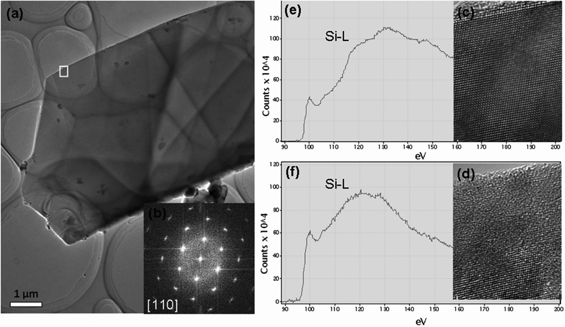 | ||
| Fig. 1 Characterization of the Si thin film. (a) Low magnification TEM images; (b) the corresponding diffraction pattern of (a); (c) and (d) HREM images before and after electron irradiation, showing the perfect crystalline structure and amorphous structure, respectively; (e) and (f) the corresponding EELS spectra obtained from the areas in (c) and (d), indicating that the amorphous structures are still retained for Si atoms. | ||
Fig. 2 shows two series of irradiation experimental results for Si with two flux values. The two experiments were carried out using the same beam dose of 6.48 × 10²³ e− cm−2 but with a different flux. The first experiment was carried out with a flux of 3.6 × 10²⁰ e− cm−2 s−1, whereas the second experiment was carried out with a flux about 3 times (i.e., 14.4 × 10²⁰ e− cm−2 s−1) that of the first experiment. The irradiation effects were observed via in situ HREM and obtained by a smaller flux, which was about 1018 e− cm−2 s−1. Fig. 2(a)–(d) shows that the crystalline character of the irradiated Si thin film still remained quite stable when the Si single crystalline thin film underwent an irradiation shower by 1800 s with a flux of 3.6 × 10²⁰ e− cm−2 s−1. However, with a higher flux of 14.4 × 10²⁰ e− cm−2 s−1 (four times that of the previous flux), the crystalline feature was damaged via the bombardment of fast electrons, as revealed in the series of HREM images from Fig. 2(e)–(h). The amorphous region became larger when the irradiation lasted for longer than 150 s, as shown in Fig. 2(f)–(h). The dashed white lines in each image of Fig. 2 show the boundaries of the amorphous region and the crystalline area. Via comparing the two experiments, it can be concluded that the c-to-a phase transition is not only dependent on electron beam current (fluence), but also dependent on flux.
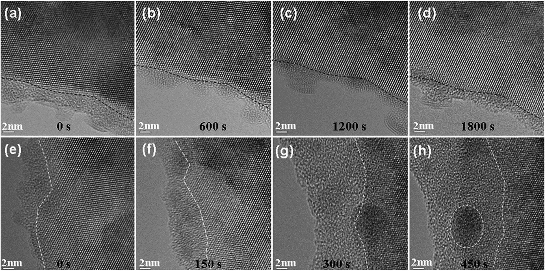 | ||
| Fig. 2 Two series of HREM images obtained from irradiation experiments. (a) Original HREM image prior to the designed electron beam illumination; (b)–(d) are the HREM images obtained after irradiation with a flux of 3.6 × 10²⁰ e− cm−2 s−1 by 600, 1200, and 1800 s, respectively. (e)–(h) are the HREM images obtained from a second experiment performed with a flux of 14.4 × 10²⁰ e− cm−2 s−1 and acquired at 0, 150, 300, and 450 s, respectively. The two irradiation experiments indicate that the different fluxes have different irradiation effects. The dotted lines show the boundary between the crystalline and amorphous structure. | ||
To systematically investigate the effect of the electron flux on phase transition during the electron beam irradiation of Si, we selected seven different electron fluxes to irradiate Si. To create a mark on the studied region, we focused the electron beam on a Si crystal of about 4 nm in diameter to puncture a hole before irradiating the specimen using these seven fluxes. Then, we studied the structural evolution of the surrounding regions of the holes. Fig. 3 shows a series of HREM images that depict the evolution process via irradiation with a flux of 10.8 × 10²⁰ e− cm−2 s−1. (a) Is an original HREM image; (b) is an HREM image obtained via irradiation by the focused electron beam with a flux of about 1 × 10²² e− cm−2 s−1. In these images, a hole with a 5 nm diameter can be clearly seen. Fig. 3(c)–(f) show four stages of irradiation with a flux of 10.8 × 10²⁰ e− cm−2 s−1; in Fig. 3(c), it was observed that the hole became small, with a diameter of about 4 nm, and the edge was amorphized. When the irradiation time was 300 s, the hole was completely filled with an amorphous material, and the crystal below the hole transformed to the amorphous state. Moreover, the edge region collapsed into the inside. When irradiation was continued, the amorphous region began to shrink. In Fig. 3(e) and (f), this trend can be observed. Recrystallization is a process of epitaxial regrowth, which could be seen from its same crystal structure. The dashed lines in Fig. 3(d)–(f) show the boundary of the amorphous region.
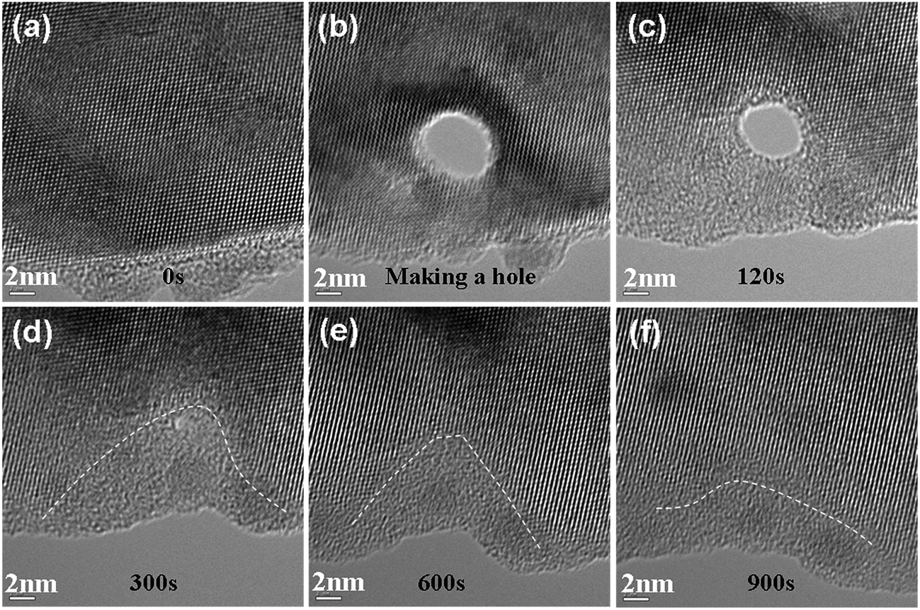 | ||
| Fig. 3 Recrystallization process of Si irradiated with a flux of 10.8 × 10²⁰ e− cm−2 s−1 observed by in situ HREM. (a) HREM image obtained in the absence of irradiation. (b) An image showing that a hole was punctured in Si by a focused electron beam with a flux of about 1 × 10²² e− cm−2 s−1. (c)–(f) Four stages of irradiation with a flux of 10.8 × 10²⁰ e− cm−2 s−1. The white dashed lines show the boundaries between the amorphous and crystalline regions, indicating the reduction of the amorphous region under irradiation. | ||
Through the abovementioned experimental results, it can be concluded that recrystallization can take place when the electron flux is relatively low. However, the amorphization process occurred when the electron flux was improved. Fig. 4 shows another series of HREM images that depict the evolutional process under electron beam irradiation with a flux of 13 × 1020 e− cm−2 s−1. The experimental process is the same as the abovementioned experiment. First, we made a hole in a perfectly crystalline Si using a focused electron beam, as indicated in Fig. 4(b). Fig. 4(a) is an original HREM image before irradiation. Fig. 4(c)–(f) show the evolutional process after irradiation with a flux of 13 × 1020 e− cm−2 s−1. In Fig. 4(c), we can see that the hole was completely filled with an amorphous material when the irradiation time was 300 s, and the edge region began to amorphize, as indicated in the A region. When irradiation was continued, the amorphous region began to extend; this was different from the abovementioned recrystallization process. The B, C, and D regions show the evolution of amorphous regions, as indicated in Fig. 4(d)–(f) respectively. Fig. 4(g) is the FFT image corresponding to the dashed framed region, which indicates the amorphous character. During the process, we can also notice that the amorphous region of the hole gradually extends. This may indicate that the amorphization process was easily carried out at the boundary between the crystal and amorphous regions.
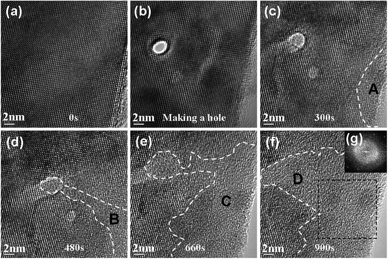 | ||
| Fig. 4 Amorphization process of Si irradiated with a flux of 13 × 1020 e− cm−2 s−1 observed by in situ HREM. (a) HREM image free from irradiation. (b) An image showing that a hole was formed in Si by a focused electron beam with a flux of about 100 × 1020 e− cm−2 s−1. (c)–(f) Show four stages of irradiation with the flux of 13 × 1020 e− cm−2 s−1. The white dashed lines show the boundaries between the amorphous and crystalline regions, indicating the extension of the amorphous region with irradiation. (g) FFT image corresponding to the dashed framed region, which indicates the amorphous character. | ||
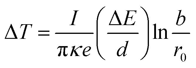
Except for the irradiation with the fluxes of 10.8 × 10²⁰ and 13 × 1020 e− cm−2 s−1, irradiation experiments were carried out under other electron fluxes, such as 3.6 × 10²⁰, 7.2 × 10²⁰, 14.4 × 10²⁰, 18 × 1020, and 21.6 × 10²⁰ e− cm−2 s−1. Before irradiation with these fluxes, a hole was firstly made by focusing the electron beam. We found that recrystallization was dominant when the flux was lower than 10.8 × 10²⁰ e− cm−2 s−1, and the velocity of recrystallization decreased with the reducing electron flux. However, when the flux was higher than 13 × 1020 e− cm−2 s−1, amorphization was dominant, and the velocity of amorphization was elevated with the increasing electron flux. The recrystallization and amorphization results are summarized in Fig. 5; Fig. 5(a) and (b) show the variation in the velocity of recrystallization/amorphization with the electron flux, respectively.
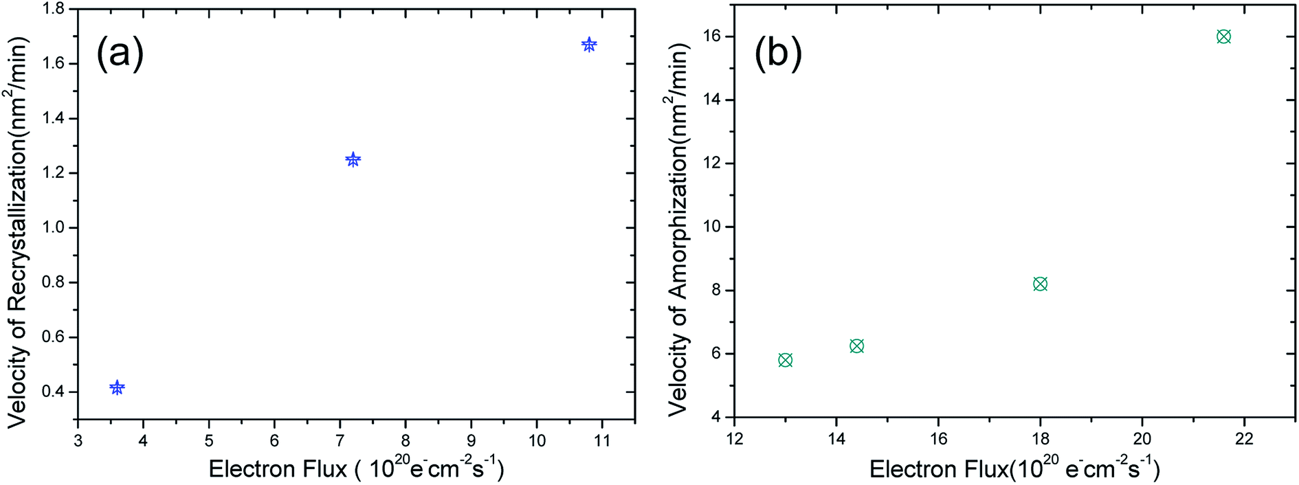 | ||
| Fig. 5 (a) and (b) reveal the variation in velocities of recrystallization/amorphization with the electron flux, respectively. In (a) and (b), the y-axis represents the velocity of recrystallization and amorphization, respectively; the x-axis represents electron flux. | ||
Compared to the previous studies indicating that the electron energy needed to be higher than 1 MeV and a temperature lower than 25 K was necessary for amorphization of Si, the present investigation indicated that the amorphization of Si could take place under a 200 kV electron irradiation and at a temperature close to room temperature. This can be attributed to the high flux provided by the field emission gun of a TEM. According to the previous studies on ion irradiation, temperature, ion mass, incident energy, and flux were the main factors that influenced the irradiation-induced amorphization process.23,35–38 However, for the investigation of electron-irradiation-induced recrystallization/amorphization of Si, the influence of flux has not been considered to date. However, our experiments clearly showed that the irradiation effect was obviously different with a same electron dose. In addition, we also demonstrated that the flux was a key factor to decide whether the amorphization/recrystallization could take place when the incident electron energy was fixed (for example, at 200 kV).
In the past, it has been well known that the electron beam irradiation itself can play two roles in materials, namely amorphization and recrystallization. The mechanisms of these two processes have been investigated for many years. Since the recrystallization and amorphization processes can be induced by a temperature effect, the temperature increase caused by electron irradiation should be considered. The temperature increase can be obtained from the following formula21
 | (1) |
In fact, when a highly energetic electron strikes the atoms of a target, many physical processes can take place,39 including ionization and displacement (knock-on) effects, which are two important irradiation effects for recrystallization or amorphization. Ionization is a process where incident electrons transfer their energy via inelastic interactions with the target atoms to induce localized electronic excitations. This ionization process alone cannot make the crystallization and/or amorphization process to happen. Many studies indicated that the ionization effect could decrease with the increasing acceleration voltage of electrons.14,40 Due to our acceleration voltage of 200 kV, which was much higher than the displacement threshold voltage 145 kV for Si,21 the ionization effect became negligible, and the knock-on effect should be considered to dominate. Above the threshold voltage, the point defects were usually described by the displaced atoms or Frenkel pairs that could be generated. Moreover, these Frenkel pairs, that is, Si interstitials (I) and vacancies (V), were mobile and could interact with each other under irradiation. When Si interstitials interacted with vacancies, it was considered that they recombined41 although there might be an energy barrier for this recombination.42,43 Thus, two competitions between generation and annihilation of IV pairs will occur.44,45 The incident electron energy, the temperature, and the flux played interdependent roles in these two competing processes. The beam current could be considered to be only a factor that affects the degree of the amorphization/recrystallization. In our research, the incident electron energy and the temperature were fixed, and the only condition that was changed was the flux. The flux, the density of fast electrons that penetrated through the irradiated specimens, determined the velocity of the generation/annihilation of IV pairs. When flux was lower than the threshold value, the annihilation velocity (Va) of IV pairs was larger than the generation velocity (Vg), and then, recrystallization occurred. With the increasing flux, the recrystallization velocity was promoted (i.e., Va > Vg, similar to the study of apatite27). Although the generation of pairs will increase, the general annihilation ability is improved due to the enhanced motion of defects when the flux is under the threshold value. Once the flux is higher than the threshold value, the generation velocity of IV pairs will exceed the annihilation velocity. Then, the amorphization was induced, and with the increasing flux, the generation velocity was far more than the annihilation velocity (Vg ≫ Va).
Note that electron irradiation will not only lead to the formation of interstitials, vacancies, and IV pairs, but also promote the complex interactions among these point defects. Many of the single IV pairs, vacancies, and interstitials were highly mobile point defects during irradiation and would not always annihilate, but clustered to form point-defect-complexes (PDC). Compared to single vacancies or IV pairs, the sizes of these PDCs were much larger, and they were more stable and acted as nucleation embryos for trapping other defects and initiating the amorphization of Si. When the electron flux was higher than the threshold values, these higher fluxes increased the generation rate of point defects, and the high point defect density enhanced the formation of PDC that promoted amorphization of Si. It should be emphasized herein that the structure of the amorphous Si could only be a distorted local structure, which slightly deviated from the perfect diamond cubic crystalline phase (six-atomic rings46) via the formation of five or seven atomic rings47 in a short range distance and retained the skeleton of the crystalline framework. Once the electron irradiation flux lowered the threshold values (i.e., at lower fluxes), the low defect density favored the reaction of inter-annihilation (i.e., the mobile interstitials or vacancies jumped into free volumes of the amorphous matrix to recover the initial crystalline network). Then, the crystallization process was initiated, and it followed an epitaxial way within the Si crystalline template. Under these threshold values of flux, the higher flux enhanced the mobility of these defects and therefore the crystallization velocity. In other words, the annihilation rate of these point defects was not constant with time, but depended in a complex way on the flux (defect density). This can also explain the previous results well. In ref. 35, on comparing the dual-irradiation (Kr+ and electron) and the Kr+ irradiation in Si, it was observed that the latter became amorphous early during the irradiation period. We considered that the irradiation via the electron beam with a flux of 5.7 × 10¹⁹ e− cm−2 s−1 promoted the recrystallization process during the dual-irradiation in their research.35 However, in ref. 19, the electron beam irradiation-induced amorphization can be considered to be derived from the larger flux of 1.8–2.6 × 10²⁰ e− cm−2 s−1, which is similar to the present study.
4. Conclusion
In conclusion, we have demonstrated two reversible processes of amorphization and recrystallization under 200 kV electron irradiation via varying the fluxes in Si. As a result, rewritable and erasable functions may be realised by using an electron beam to change the fluxes for Si applications. Moreover, the study provides insight into the amorphization and recrystallization mechanisms of Si under a radiation environment.Acknowledgements
This work was supported by the National Natural Science Foundation of China (11374029) and the Key Project of National Natural Science Foundation of China (11234011).References
- F. Banhart and P. Ajayan, Nature, 1996, 382, 433 CrossRef CAS.
- A. Krasheninnikov and F. Banhart, Nat. Mater., 2007, 6, 723 CrossRef CAS PubMed.
- S. Xu, M. Tian, J. Wang, J. Xu, J. M. Redwing and M. H. Chan, Small, 2005, 1, 1221 CrossRef CAS PubMed.
- X. D. Wei, D. M. Tang, Q. Chen, Y. Bando and D. Golberg, ACS Nano, 2013, 7, 3491 CrossRef CAS PubMed.
- J. A. Rodriguez-Manzo and F. Banhart, Nano Lett., 2009, 9, 2285 CrossRef CAS PubMed.
- S. Sood, K. Kisslinger and P. Gouma, J. Am. Ceram. Soc., 2014, 97, 3733 CrossRef CAS.
- M. Zhu, M. J. Xia, Z. T. Song, Y. Cheng, L. C. Wu, F. Rao, S. N. Song, M. Wang, Y. G. Lu and S. L. Feng, Nanoscale, 2015, 7, 9935 RSC.
- K. Zheng, C. C. Wang, Y. Q. Cheng, Y. H. Yue, X. D. Han, Z. Zhang, Z. W. Shan, S. X. Mao, M. Ye and Y. D. Yin, Nat. Commun., 2010, 1, 1 CrossRef PubMed.
- J. F. Zang, L. H. Bao, R. A. Webb and X. D. Li, Nano Lett., 2011, 11, 4885 CrossRef CAS PubMed.
- L. H. Wang, X. D. Han, P. Liu, Y. H. Yue, Z. Zhang and E. Ma, Phys. Rev. Lett., 2010, 105, 135501 CrossRef PubMed.
- L. H. Wang, P. Liu, P. F. Guan, M. J. Yang, J. L. Sun, Y. Q. Cheng, A. Hirata, Z. Zhang, E. Ma and M. W. Chen, Nat. Commun., 2013, 4, 2413 Search PubMed.
- L. H. Wang, J. Teng, P. Liu, A. Hirata, E. Ma, Z. Zhang, M. W. Chen and X. D. Han, Nat. Commun., 2014, 5, 4402 CAS.
- A.-A. El Mel, L. Molina-Luna, M. Buffiere, P.-Y. Tessier, K. Du, C.-H. Choi, H.-J. Kleebe, S. Konstantinidis, C. Bittencourt and R. Snyders, ACS Nano, 2014, 8, 1854 CrossRef CAS PubMed.
- L. Hobbs and M. Pascucci, J. Phys, 1980, 41, C6 Search PubMed.
- H. Inui, H. Mori, T. Sakata and H. Fujita, J. Non-Cryst. Solids, 1990, 116, 1 CrossRef CAS.
- H. Inui, H. Mori, A. Suzuki and H. Fujita, Philos. Mag. B, 1992, 65, 1 CAS.
- W. L. Gong, L. M. Wang, R. Ewing and J. Zhang, Phys. Rev. B, 1996, 54, 3800 CrossRef CAS.
- R. Devanathan, T. D. de la. Rubia and W. Weber, J. Nucl. Mater., 1998, 253, 47 CrossRef CAS.
- S. Takeda and J. Yamasaki, Phys. Rev. Lett., 1999, 83, 320 CrossRef CAS.
- M. Ishimaru, I.-T. Bae and Y. Hirotsu, Phys. Rev. B, 2003, 68, 144102 CrossRef.
- I. Jencic, M. Bench, I. Robertson and M. Kirk, J. Appl. Phys., 1995, 78, 974 CrossRef CAS.
- L. M. Wang and W. Weber, Philos. Mag. A, 1999, 79, 237 CAS.
- S. X. Wang, L. M. Wang and R. C. Ewing, Phys. Rev. B, 2000, 63, 024105 CrossRef.
- J. Yamasaki, S. Takeda and K. Tsuda, Phys. Rev. B, 2002, 65, 115213 CrossRef.
- T. Nagase and Y. Umakoshi, Scr. Mater., 2003, 48, 1237 CrossRef CAS.
- Y. W. Zhang, J. Lian, C. M. Wang, W. L. Jiang, R. C. Ewing and W. J. Weber, Phys. Rev. B, 2005, 72, 094112 CrossRef.
- I.-T. Bae, Y. Zhang, W. J. Weber, M. Higuchi and L. A. Giannuzzi, Appl. Phys. Lett., 2007, 90, 021912 CrossRef.
- S. Suzuki, K. Kanzaki, Y. Homma and S.-y. Fukuba, Jpn. J. Appl. Phys., 2004, 43, L1118 CrossRef CAS.
- R. Egerton, P. Li and M. Malac, Micron, 2004, 35, 399 CrossRef CAS PubMed.
- J. H. Choi, J. Lee, S. M. Moon, Y.-T. Kim, H. Park and C. Y. Lee, J. Phys. Chem. Lett., 2016, 7, 4739 CrossRef CAS PubMed.
- P. Ecton, J. Beatty, G. Verbeck, W. Lakshantha, B. Rout and J. Perez, Appl. Surf. Sci., 2016, 387, 822 CrossRef CAS.
- X. D. Han, Y. F. Zhang, K. Zheng, X. N. Zhang, Z. Zhang, Y. J. Hao, X. Y. Guo, J. Yuan and Z. L. Wang, Nano Lett., 2007, 7, 452 CrossRef CAS PubMed.
- X. D. Han, K. Zheng, Y. F. Zhang, X. N. Zhang, Z. Zhang and Z. L. Wang, Adv. Mater., 2007, 19, 2112 CrossRef CAS.
- K. Zheng, X. D. Han, L. H. Wang, Y. F. Zhang, Y. H. Yue, Y. Qin, X. N. Zhang and Z. Zhang, Nano Lett., 2009, 9, 2471 CrossRef CAS PubMed.
- D. Seidman, R. Averback, P. Okamoto and A. Baily, Phys. Rev. Lett., 1987, 58, 900 CrossRef CAS PubMed.
- P. J. Schultz, C. Jagadish, M. Ridgway, R. Elliman and J. Williams, Phys. Rev. B, 1991, 44, 9118 CrossRef CAS.
- R. Goldberg, J. Williams and R. Elliman, Mater. Res. Soc., 1993, 321, 417 CrossRef.
- R. Goldberg, J. Williams and R. Elliman, Nucl. Instrum. Methods Phys. Res., Sect. B, 1995, 106, 242 CrossRef CAS.
- F. Banhart, Rep. Prog. Phys., 1999, 62, 1181 CrossRef CAS.
- G. Das and T. Mitchell, Radiat. Eff., 1974, 23, 49 CrossRef CAS.
- L. Pelaz, M. Jaraiz, G. Gilmer, H.-J. Gossmann, C. Rafferty, D. Eaglesham and J. Poate, Appl. Phys. Lett., 1997, 70, 2285 CrossRef CAS.
- M. Tang, L. Colombo, J. Zhu and T. D. De La Rubia, Phys. Rev. B, 1997, 55, 14279 CrossRef CAS.
- L. A. Marqués, L. Pelaz, J. Hernández, J. Barbolla and G. H. Gilmer, Phys. Rev. B, 2001, 64, 045214 CrossRef.
- L. A. Marqués, L. Pelaz, M. Aboy, L. Enríquez and J. Barbolla, Phys. Rev. Lett., 2003, 91, 135504 CrossRef PubMed.
- L. Pelaz, L. A. Marqués, M. a. Aboy, J. Barbolla and G. H. Gilmer, Appl. Phys. Lett., 2003, 82, 2038 CrossRef CAS.
- J. W. Corbett, J. P. Karins and T. Y. Tan, Nucl. Instrum. Methods, 1981, 182, 457 CrossRef.
- P. Steinhardt, R. Alben and D. Weaire, J. Non-Cryst. Solids, 1974, 15, 199 CrossRef CAS.
| This journal is © The Royal Society of Chemistry 2017 |