
 Open Access Article
 This Open Access Article is licensed under a
 Creative Commons Attribution 3.0 Unported Licence
Mn doped CdS passivated CuInSe2 quantum dot sensitized solar cells with remarkably enhanced photovoltaic efficiency
Ikhtisham Mehmood†
a,
Yueli Liu†a,
Keqiang Chena,
Abdul Hakim Shahb and
Wen Chen *a
*a
aState Key Laboratory of Advanced Technology for Materials Synthesis and Processing, School of Materials Science and Engineering, Wuhan University of Technology, Wuhan 430070, P. R. China. E-mail: chenw@whut.edu.cn; Fax: +86-27-87760129; Tel: +86-27-87651107
bDepartment of Material Physics and Nanotechnology, Khushal Khan Khattak University, Karak 27200, Pakistan
First published on 30th June 2017
Abstract
Here we address the optoelectronics properties of CuInSe2 and Mn doped CdS quantum dot (CISe/Mn-CdS QD) passivated layer solar cells. CISe/Mn-CdS QD solar cells exhibit a remarkably enhanced optical absorption in the visible region as well as monochromatic incident photon-to-electron conversion efficiency (IPCE) (up to 40–90%), which present the interesting photovoltaic efficiency of 3.96% under one sun illumination. Such remarkable optical behavior of the CISe/Mn-CdS QD passivated solar cells is explained by an optical mechanism based on an energy band model and valid physical laws.
1. Introduction
Quantum dot sensitized solar cells (QDSSCs) own many multi-dimensional characteristics, such as size tunable band gaps, ultrafast electron transfer, multi-exciton generation (MEG), high absorption and surpassing the Shockley–Queisser limit (32%), which have attracted the profound attention of researchers over the last few decades.1,2 Based on these exciting properties, Cd and Pb-based QDSSCs (CdS, CdSe, CdS/CdTe and PbS, etc.) have been found to exhibit a power conversion efficiency (PCE) in the range of 4–9%.3–7 Zhong's group has obtained a PCE of 9.73% for a metal hydroxide coated CdSeTe photoanode.8 Furthermore, an enhanced PCE of 11% has been reported for the CdSeT QDSSCs with a carbon counter electrode.9 However, the toxic natures of Cd and Pb and the midgap trapping in Pb limit their commercial applications.10,11In order to solve these problems, researchers have shown their devotion towards the ternary semiconductor quantum dots (TQDs) in photovoltaic devices due to their non-toxic nature, narrow band gap, broad band light harvesting and low cost, such as CuInS2, CuInSe2, AgInS2, etc.12–14 Among these materials, CuInSe2 quantum dots (CISe QDs) with the narrow band gap (1.04 eV) have been found to effectively enhance the photovoltaic performance of the QDSSCs due to the large exciton Bohr's radius, which matches well with the solar spectrum.15–18 Till now, various techniques have been reported to synthesize the CuInSe2 QDs for using in QDSSCs,19–21 which include the controllable solvothermal method by incorporating the use of diphenyl phosphine selenide as Se precursor17 and oleylamine as a solvent and capping ligand.20 Recently, Zhong's group have incorporated Zn in the CISe to obtain the absorption spectra at 1000 nm with PCE at the range of 9%.22 Efficiency has been further enhanced to be 12% by nitrogen doped mesoporous carbon counter electrode in Zn–Cu–In–Se quantum dots sensitized solar cells.23 However, these QDSSCs still suffer from the issues of low efficiency and poor stability under drastic condition comparing with the conventional solar cells. Therefore, some new areas are required to obtain stable and efficient structure in QDSSCs. These solar cells still need to obtain the optimal structure and fulfill the demanding of the industrial applications.
In order to improve the optical and electrical properties of QDSSCs, various deposition approaches have been employed for the loading and passivation of QDs on the surface of TiO2 matrix. In situ chemical bath deposition (CBD), successive ionic layer adsorption and reaction (SILAR) method,24–26 and ex situ assembly linking technique4 are commonly applied techniques. The surface passivation of QDs by semiconductor materials with large band gap such as CdS and ZnS is carried out to enhance the stability of QDs surface and photovoltaic performance by the prevention of leakage current, which delivers a significant power conversion efficiency (PCE),20,27,28 and high open circuit voltage (Voc).13 The advantage of the Mn2+ doping creates an additional electronic state in the CdS host material, which reduces electron–hole recombination and increases a short current density of the QDSSCs. Furthermore, the Mn has dorbital (4T1–6A1) spin and orbital forbidden states, which increase the life time of the excited electron.29 In addition, this type of the engineering structure controls the interfacial charge recombination and updates PCE of the cell. The midgap state originated from Mn doping induces the electron to be trapped, which screens them from the recombination with holes and oxidized polysulfide electrolyte.29 Moreover, the addition of the dopant materials elevates the PCE value upto 5.4–9.0% by changing the energy level in case of Mn doped CdS/CdSe and ZnS/SiO2 QDSSCs.27,29 Therefore, the engineering of Mn-doped material will greatly enhance the PCE of the QDSSCs.
Herein, we employ a low temperature and simple thermolysis method, followed by the capping of bifunctional molecule to prepare mercaptopropionic acid (MPA) capped CISe QDs, and the CISe QDs are sensitized on TiO2 matrix by in situ linker assisted technique. Furthermore, the passivation layer of Mn-doped CdS (Mn-CdS) QDs over CISe QDs/TiO2 matrix is carried out by SILAR method.27 The doping produces a stable structure under severe temperature condition and fast electron transfer. These CISe/Mn-CdS QD passivated QDSSCs exhibit significant optical and electrical properties under one sun illumination.
2. Experimental
2.1 Synthesis of CuInSe2 QDs
All chemicals were analytically grade and were used without further purifications. CuInSe2 QDs were synthesized by a modified thermolysis method as reported in literature.18 Briefly, 10 mL oleylamine (OLA), 1 mmol CuI (0.190 g) and 1 mmol InCl3 (0.220 g) were simultaneously added to a three neck flask and degassed for 30 minutes. Then, the temperature was increased to 180 °C under the argon flow and 2 mmol DPP/Se (1![[thin space (1/6-em)]](https://www.rsc.org/images/entities/char_2009.gif) :1 ratio) was injected and the temperature was maintained at 180 °C for a further 10 minutes. The mixed solution was cooled to room temperature and washed by centrifugation through methanol and hexane for three times. The precipitates were dried at 100 °C in vacuum oven to obtain the CISe QDs powder.
:1 ratio) was injected and the temperature was maintained at 180 °C for a further 10 minutes. The mixed solution was cooled to room temperature and washed by centrifugation through methanol and hexane for three times. The precipitates were dried at 100 °C in vacuum oven to obtain the CISe QDs powder.
The as-prepared CISe QDs were dispersed in fresh hexane for sensitization. To obtain MPA capped QDs, CISe QDs/methanol solution (1 mL) was dissolved in methanol solution of MPA and NaOH, which was stirred for 30 minutes, then deionized water was added to the mixture and maintained stirring for further 20 minutes. The precipitates were finally washed through centrifugation in excess acetone and deionized water to obtain water soluble MPA capped CISe QDs.
2.2 Device fabrication
TiO2 nanoparticle working electrodes were prepared by screen printing technique as reported in literature.30 Briefly, fluorine doped tin oxide (FTO) glass was first treated with TiCl4 solution at 70 °C for 3 minutes. Back scattering layer was prepared from P25 paste, followed by the top layer of 400 nm TiO2 nanoparticles. Finally, the TiO2 thin films were sintered at 450 °C in the muffle furnace, and then dipped in CISe QDs solution for 24 hours to complete the sensitization. These CISe QDs sensitized TiO2 films were washed by water and dried under vacuum.MPA capped CISe QDs were sensitized on TiO2 films followed by the passivation of Mn-CdS layer by successive ionic layer adsorption and reaction (SILAR) method. In short, 0.1 M cadmium nitrate in methanol was used as cation source and 0.1 M sodium sulfide in 1:1 methanol and water as anion source. To incorporate Mn doping, manganese acetate (0.075 M) was mixed with cadmium nitrate. The CISe QDs sensitized films were immersed for one minute in Mn doped Cd precursor followed by rainsing with methanol, and then immersed in S precursor followed by rinsing with methanol, which counts as one SILAR cycle and repeats the process for 3 cycles. Finally the devices were dried under Ar atmosphere to remove the organic solvents.
The QDs co-sensitized solar cells were fabricated by assembling the sensitized TiO2 photoanode and brass based Cu2S counter electrode with a binder clip, separated by a 60 mm Scotch tape spacer. Polysulfide electrolyte solution with composition of Na2S (2.0 M), S (2.0 M) powder and KCl (0.2 M) was injected into the cells device.
2.3 Characterization and measurements
Structure and morphology were measured by X-rays diffraction analysis (XRD, Pertpro, PANalytical, Netherlands) using Cu Kα, field emission scanning electron microscope (FESEM, JSEM-5610LV, Japan) and the high resolution transmission electron microscope (HRTEM, JEM-2100F, JEOL, Japan), respectively. The optical characterization of the samples was carried out by using UV-vis absorption spectra (UV-2550, Shimadzu, Japan). The photocurrent density–voltage (J–V) curves of the QDSSCs were measured by the Keithley 4200 semiconductor characterization system (Keithley Instruments, USA) under simulated AM 1.5 illumination (Newport 91160, 300 W xenon lamp, USA). The incident photon-to-current conversion efficiency (IPCE) was measured using Newport's IPCE Measurement Kit under the monochromatic light from a monochromator (Newport). The electrochemical impedance spectra (EIS) were measured by using an impedance analyzer (Auto lab PGSTAT320N) at open-circuit potentials under AM 1.5 illumination.3. Results and discussions
XRD pattern of CISe QDs is shown in Fig. 1(a), and the diffraction peaks are indexed to the chalcopyrite (tetragonal) CuInSe2 QDs (JCPDS 00-051-1221) with all major peaks reflected from (112), (204), (312) and minor peak of (211) crystal plane at angle 2θ of 26.77°, 44.43°, 54.64° and 31.01°, respectively, which is the stable phase of CISe QDs at room temperature. The significant broadening in the peaks represents the small size of CuInSe2 QDs. Applying Scherrer's formula, the average size of QDs is calculated to be 5 nm.31 Fig. 1(b) and(c) illustrate the top and cross sectional views of the as-prepared film with the thickness of 6 μm. Average size of as-synthesized QDs is 5 nm as shown in the Fig. 1(d), which is in good agreement with the XRD analysis. The HRTEM image displays high crystallinity of the as-synthesized CISe QDs in Fig. 1(e), and the inter-planner spacing is about 0.362 nm, which corresponds to the (112) crystal plane of the tetragonal structure.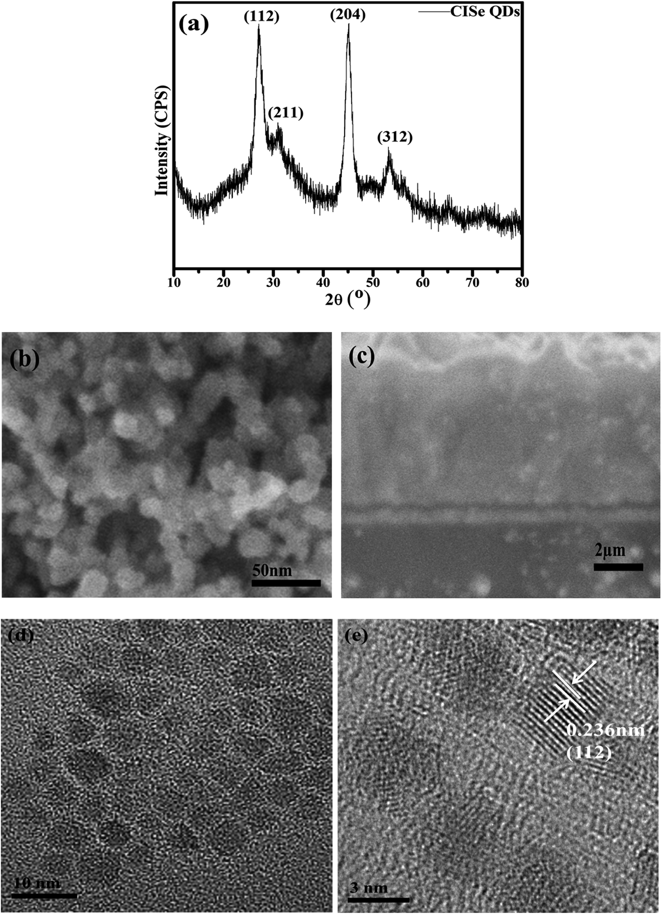 | ||
| Fig. 1 Characteristic of the as-prepared CuInSe2 quantum dots: (a) XRD pattern, (b) top and (c) cross-sectional views of FESEM images, (d) TEM image, (e) HRTEM image. | ||
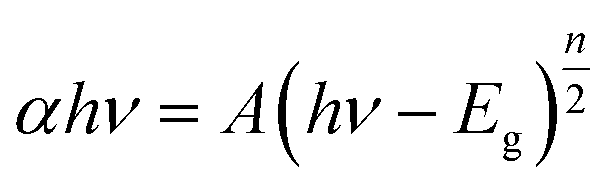
UV-vis spectra of the TiO2 photoanodes sensitized by CISe, CdS, Mn-CdS and CISe/Mn-CdS QDs are shown in Fig. 2(a). After the sensitization of CISe QDs, the absorption spectrum of the TiO2 films is significantly enhanced both in ultraviolet and visible light regions. The obvious blue shift is observed after the sensitization of CISe QDs with the main peak centered at 450 nm, while the absorption onsets of the TiO2/CdS and TiO2/Mn-CdS occur approximately at 560 and 580 nm, respectively, which show the characteristics spectra toward red shift compared with that of the bulk CdS material. The CISe/Mn-CdS QD passivated electrode exhibits red-shift absorption at the wavelength range of 650–700 nm. Mn-CdS passivation layer has an absorption onset at 580 nm, the red-shift phenomenon must result from the light absorption of the CISe QDs. The passivation enhances the absorption spectra towards long wavelength region comparing with those of pure TiO2 and CISe/TiO2 matrix. This red-shift may indicate that the QDs charge carriers wave functions tunnel into the surrounding CdS shell. The broad spectrum reveals the heterogeneity of the CISe and Mn-CdS QDs sizes.32 Furthermore, UV-vis spectra are also measured to reveal the band gaps of the as-prepared samples. Herein, using Tauc relation (eqn (1)), the optical band gap of CISe QDs is calculated as 1.38 eV and other corresponding materials are shown in Fig. 2(b).33,34
 | (1) |
 | ||
| Fig. 2 (a) UV-vis spectra of TiO2, CISe, CdS, Mn-CdS and CISe/Mn-CdS QDs sensitized solar cells, (b) the Tauc plots for the determination the band gap. | ||
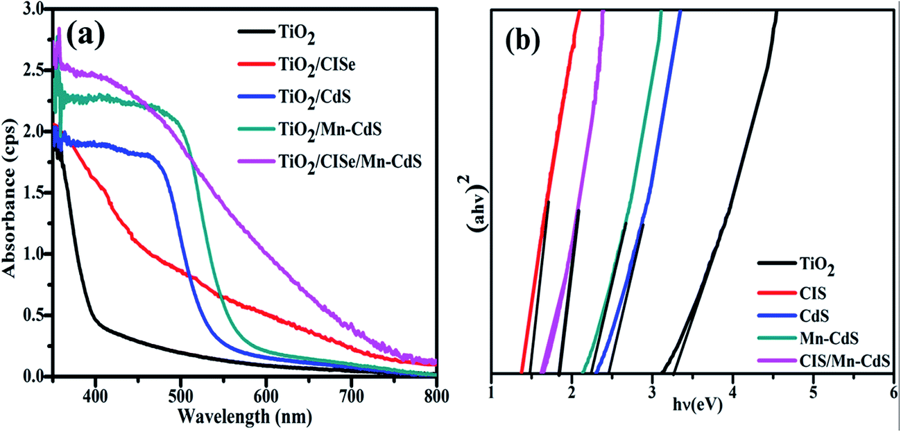
The photovoltaic performance is determined from the current–voltage (J–V) characteristics of the assembled devices as shown in the Fig. 3(a). The photovoltaic parameters of these solar cells, such as the open circuit potential (Voc), short circuit current density (Jsc), fill factor (FF) and power conversion efficiency (PCE), are listed in Table 1. The photovoltaic efficiencies of CISe QDs, CdS QDs, Mn-CdS QDs and CISe/Mn-CdS QD passivate solar cells are 0.80, 1.98, 3.08 and 3.96%, respectively. For CISe/Mn-CdS QD passivate solar cells, the decreasing of the FF to 41% clearly indicates the reduction in the internal charge recombination and defect state in the QDSSCs.18 Moreover, the increasing in the current density reveals the high charge transportation in photovoltaic device. CISe/Mn-CdS QD passivate solar cells exhibit an enhanced open circuit voltage of 0.59 V, which substantiates a high charge extraction in the alloy structure. However, the obtained photovoltaic efficiency in the present work is still lower comparing with some of similar works.8,18,22,29
 | ||
| Fig. 3 The photovoltaic performance of the CISe, CdS, Mn-CdS and CISe/Mn-CdS sensitized solar cells under AM 1.5 sunlight: (a) J–V curves, (b) IPCE curves. | ||
| Type | Voc (V) | Jsc (mA cm−2) | FF | Efficiency (%) |
|---|---|---|---|---|
| CISe QDS | 0.53 | 3.50 | 43 | 0.80 |
| CdS QDs | 0.51 | 7.20 | 52 | 1.98 |
| Mn-CdS QDs | 0.56 | 10.26 | 49 | 3.08 |
| CISe/Mn-CdS QDS | 0.59 | 16.10 | 41 | 3.96 |
Normally, the PCE value of QDSSCs is greatly influenced by the light absorption ability, which is related with the sensitization ratio of QDs as well as the size and morphology of the photoanode film. In our case, as the passivation of Mn-CdS QDs inside the pores of CISe QDs influences the electrolyte diffusion inside the photoanodes, which leads to lower the charge diffusion and ultimately limit the cell performance.35 The lower diffusion length causes the decreasing of the number of the extracted electrons to the TiO2 matrix. Conduction band level of CISe QDs is lower than that of n-type Mn-CdS QDs, which reduces the charge transfer across the CISe/Mn-CdS interface to cause a low photovoltaic performance.36 In our case, the SILAR and CBD deposition may lead to the undesired defect state due to the broad size distribution, thereby, the undesired surface defects are created, which leads to the trapping of charge carrier and the decreasing of the PCE value.29,37
IPCE is measured for electrons extraction/collection excited by incident photons as shown in Fig. 3(b). IPCE values of CISe, CdS, Mn-CdS and CISe/Mn-CdS QDSSCs show high values even in longer wavelength regions, and good consistency with the absorption spectra as shown in Fig. 2(a), which confirms the large number of electrons transport to the TiO2. The lower IPCE values of the CdS and Mn-CdS sensitized solar cells are due to their weak response at low energy wavelength.38 The enhancement in the IPCE value is noted for CISe/Mn-CdS QDSSCs with a maximum IPCE in the range of 40–90% with the obtained power conversion efficiency of 3.96%. This high response of incident photon to excite electrons conversion is due to the narrow band gap of CISe QDs, which can deduce a high electron injection upon the incident light photon. Moreover, the passivation of Mn-doped CdS QDs improves the performance of electron collection/injection, as the large number of the photo-induced electrons in CISe/Mn-CdS QDSSCs are injected into and then collected efficiently on TiO2 matrix. The high photoresponses in short and long wavelength regions are due to the combination of narrow and wide band gap CISe/Mn-CdS heterostructure, which absorbs the light in both of ultraviolet and visible regions. The photoresponse can be calculated by the following equation.39
| IPCE = LHE × ϕinj × ηcc | (2) |
QD loading ratio on the TiO2 surface is an important factor for high photovoltaic performance. The advantage of in situ chemicals bath deposition method is the insertion of the small size QDs in the space between TiO2 nanoparticles, thereby reduces the defect levels and electron–hole recombination, which ultimately enhances the photovoltaic performance. Firstly, MPA is a short chain ligand, which acts as the linker molecule between QDs and TiO2 thin film through a strong interaction of (Ti–O–Ti) with carboxyl group (COOH). Secondly, SH group of MPA firmly interacts with Cu ion through S-metal junction.4 Thirdly, according to soft and hard acid basis theory, Se2− ions have a strong binding with soft ions-SH from MPA.40 The MPA capped and water soluble CISe QDs have a strong affinity to the TiO2 molecules. Moreover, under the simulated sunlight irradiation, the MPA linking effectively reduces the blocking of photo-induced electrons transfer and the recombination possibility of photo-induced electrons and holes, which results in the improvement of photovoltaic conversion efficiency.41
Electrical impedance spectra (EIS) expose the dynamics of bound or mobile charge in bulk or interfacial region inside the solar cells. The EIS measurements are carried out under the dark condition at different forward biases ranging from 0 to −0.5 V. Nyquist plots of the cells at forward biased −0.5 V are shown in the Fig. 4. Comparing with the Nyquist plots of CISe, CdS and Mn-CdS QDSSCs, the CISe/Mn-CdS QDSSCs reveal a high Rrec value, suggesting a considerably larger electron transport resistance between the photo-electrode and polysulfide electrolyte.32 The Rs values of all the electrodes are nearly same, which is attributed to the fact that the passivation has no effect on the interfaces. Small semicircle of Mn-CdS QDSSCs indicates the favor of electron transfer from Mn-CdS QDs to the TiO2 matrix. The low resistance feature of the Mn-CdS QDs may be due to the forbidden d–d orbital transition, which impulses the transportation electron and lowers the resistance. The large semicircle of CISe/Mn-CdS QDSSCs shows the high interface resistance, which is the sum of the resistances among Mn-CdS QDs, CISe QDs and TiO2 interfaces in the QDSSCs and increases with the increasing of the film thickness. However, the surface defect and dangling bonds of the TiO2 film are removed by the Mn-CdS growth, which ultimately suppresses the photo-induced electron–hole recombination. In comparison with the other electron deterring approaches, the CISe/Mn-CdS alloy structure in our work exhibits a compelling performance in reducing the charge recombination and improving power conversion efficiency. The high recombination resistance of the Mn-CdS passivated CISe QDSSCs is possibly originated due to the surface trap states, which favor for the recombination to lower the PCE value of the device. The simulated results of the as-prepared samples are listed in the Table 2. These results confirm that the passivation of Mn-CdS QDs on CISe QDSSCs is an effective tool to suppress the charge recombination. It eventually contributes to the excellent properties of QDSSCs.
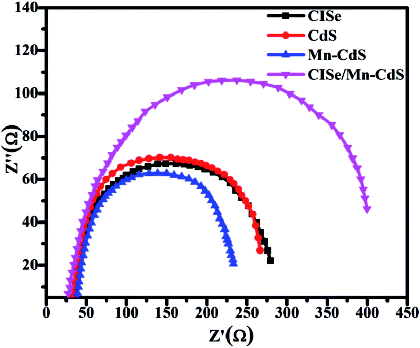 | ||
| Fig. 4 EIS plots of CISe, CdS, Mn-CdS and CISe/Mn-CdS sensitized solar cells. | ||
| Sample | RS (Ω cm2) | Cμ (mF cm−2) | Rrec (Ω cm2) |
|---|---|---|---|
| CISe QDSSCs | 30.54 | 0.51 | 285.9 |
| CdS QDSSCs | 30.20 | 0.46 | 271.4 |
| Mn-CdS QDSSCs | 36.30 | 0.54 | 223.8 |
| CISe/Mn-CdS QDSSCs | 24.80 | 0.72 | 443.0 |
Under the sun light irradiation with sufficient energy, the photo-induced electrons jumps from valence band (VB) to conduction band (CB) of Mn-CdS QDs. Due to the large band gap offset, the photo-induced electrons transfer from the Mn-CdS CB to CuInSe2 CB and then to TiO2 CB, which increases the photocurrent density. Furthermore, the photo-generated electrons from the CB of CuInSe2 QDs and Mn-CdS QDs with the high absorption of sun light transfer to TiO2 CB, which corporately increase the current density of the optoelectronic device. Hereafter, it is clearly observed that Mn doping causes the delay of the photo-induced electrons in the excited state, thereby enhances Voc. Schematic diagram of the photo-induced electron flow is enlightened in Fig. 5. Mn doped CdS QDs create some states in the mid-bandgap region due to the d atomic orbitals of Mn (4T1–6A1). However, the transitions between these two energy levels (4T1–6A1) are both spin and orbital forbidden.27 Thereby, the photo-induced electrons stay for a long time at Mn d-states and then are injected to CISe QDs as well as to TiO2. There are some additional deep electron trap states, which reduce the concentration of mobile carriers in the n-type CdS layer. The generation of the excitons in the CdS QDs causes a compensation of deep trap by ‘photo-doping’,42,43 which increases the number of mobile carriers, hence reduces the barrier towards electron transport across the CdS QDs and leads to an increased junction conductance.44 Mn-CdS QDs have a higher mobility of photo-induced electrons than CdS QDs, which increases the current density of the Mn-CdS QDSSCs. Furthermore, the long life time of d–d transition in Mn delays the electron–hole recombination in the QDs, which alternately increases the open circuit potential.
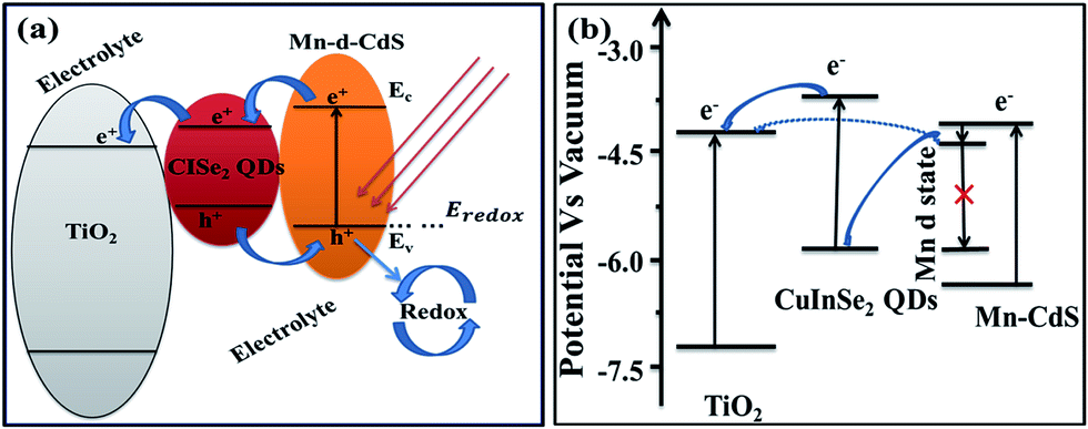 | ||
| Fig. 5 Schematic diagrams of CISe/Mn-CdS sensitized solar cells: (a) band gap, (b) electron transport path. | ||
4. Conclusion
Water soluble CISe QDs of 5 nm are prepared by a simple thermolysis method. Co-sensitization of CISe/Mn-CdS QDs clearly enhances the optical and electrochemical properties of the solar cells. The excellent architecture of CISe/Mn-CdS demonstrates the outstanding light-harvesting behavior of the QDSSCs. MPA-capping improves the QDs loading on TiO2 photoanode. The combination of in situ linker and SILAR method in the fabrication of CISe/Mn-CdS alloy architecture suppresses the photo-induced electron–hole recombination; as a result, the photovoltaic efficiency of 3.96% is achieved for CISe/Mn-CdS QDSSCs.Acknowledgements
This work is supported by the National Nature Science Foundation of China (No. 11674258, 51506155), International Science & Technology Cooperation Program of China (No. 2013DFR50710), the National Nature Science Foundation of Hubei Province (No. 2014CFB165, 2015CKC898), the Fundamental Research Funds for the Central Universities (No. 2017II22GX) and Applied Basic Research Program of Wuhan (No. 2016010101010020). Thanks for the measurements supporting from Center for Materials Research and Analysis at Wuhan University of Technology (WUT).References
- A. Kongkanand, K. Tvrdy, K. Takechi, M. Kuno and V. Prashant, J. Am. Chem. Soc., 2008, 130, 4007–4015 CrossRef CAS PubMed.
- C. J. Stolle, T. B. Harvey, D. R. Pernik, J. I. Hibbert, J. Du, D. J. Rhee, V. A. Akhavan, R. D. Schaller and B. A. Korgel, J. Phys. Chem. Lett., 2014, 5, 304–309 CrossRef CAS PubMed.
- X. Y. Yu, B. X. Lei, D. B. Kuang and C. Y. Su, J. Mater. Chem., 2012, 22, 12058–12063 RSC.
- H. Zhang, K. Cheng, Y. M. Hou, Z. Fang, Z. X. Pan, W. J. Wu, J. L. Hua and X. H. Zhong, Chem. Commun., 2012, 48, 11235–11237 RSC.
- V. G. Pedro, C. Sima, G. Marzari, P. P. Boix, S. Gimenez, Q. Shen, T. Dittrich and I. M. Sero, Phys. Chem. Chem. Phys., 2013, 15, 13835–13843 RSC.
- J. Yang, J. Wang, K. Zhao, T. Izuishi, Y. Li, Q. Shen and X. Zhong, J. Phys. Chem. C, 2015, 119, 28800–28808 CAS.
- K. Zhao, Z. Pan, I. Mora-Sero, E. Canovas, H. Wang, Y. Song, X. Gong, J. Wang, M. Bonn, J. Bisquert and X. Zhong, J. Am. Chem. Soc., 2015, 137, 5602–5609 CrossRef CAS PubMed.
- Z. Du, Z. Pan, F. Santiago, K. Zhao, D. Long, H. Zhang, Y. Zhao, X. Zhong, J. Yu and J. Bisquert, J. Phys. Chem. Lett., 2016, 7, 3103–3111 CrossRef CAS PubMed.
- Z. Ren, Z. Wang, R. Wang, Z. Pan, X. Gong and X. Zhong, Chem. Mater., 2016, 28, 2323–2330 CrossRef CAS.
- J. Zhang, R. G. Du, Z. Q. Lin, Y. F. Zhu, Y. Guo, H. Q. Qi, L. Xu and C. J. Lin, Electrochim. Acta, 2012, 83, 59–64 CrossRef CAS.
- J. W. Lee, D. Y. Son, T. K. Ahn, H. W. Shin, I. Y. Kim, S. J. Hwang, M. J. Ko, S. Sul, H. Han and N. G. Park, Sci. Rep., 2013, 3, 1050 CrossRef PubMed.
- T. Omata, K. Nose and O. Y. M. Shinya, J. Appl. Phys., 2009, 105, 073106 CrossRef.
- D. V. Talapin, J. S. Lee, M. V. Kovalenko and E. V. Shevchenko, Chem. Rev., 2010, 110, 389–458 CrossRef CAS PubMed.
- B. Chen, H. Zhong and B. Zou, Prog. Chem., 2011, 23, 2276–2286 CAS.
- Z. Pan, I. Sero, Q. Shen, H. Zhang, Y. Li, K. Zhao, J. Wang, X. Zhong and J. Bisquert, J. Am. Chem. Soc., 2014, 136, 9203–9210 CrossRef CAS PubMed.
- H. Zhong, Z. Wang, E. Bovero, Z. Lu, F. C. J. M. Van Veggel and G. D. Scholes, J. Phys. Chem. C, 2011, 115, 12396–12402 CAS.
- M. G. Panthani, C. J. Stolle, D. K. Reid, D. J. Rhee, T. B. Harvey, V. A. Akhavan, Y. Yu and B. A. Korgel, J. Phys. Chem. Lett., 2013, 4, 2030–2034 CrossRef CAS PubMed.
- W. Li, Z. Pan and X. Zhong, J. Mater. Chem. A, 2015, 3, 1649–1655 CAS.
- Q. Wang, J. Qiao, J. Zhou and S. Gao, Electrochim. Acta, 2015, 167, 470–475 CrossRef CAS.
- C. F. Du, T. You, L. Jiang, S. Q. Yang, K. Zou, K. L. Han and W. Q. Deng, RSC Adv., 2014, 4(64), 33855–33860 RSC.
- M. G. Panthani, V. Akhavan, B. Goodfellow, J. P. Schmidtke, L. Dunn, A. Dodabalapur, P. F. Barbara and B. A. Korgel, J. Am. Chem. Soc., 2008, 130, 16770–16777 CrossRef CAS PubMed.
- J. Du, Z. Du, J. S. Hu, Z. Pan, Q. Shen, J. Sun, D. Long, H. Dong, L. Sun, X. Zhong and L. J. Wan, J. Am. Chem. Soc., 2016, 138, 4201–4209 CrossRef CAS PubMed.
- S. Jiao, J. Du, Z. Du, D. Long, W. Jiang, Z. Pan, Y. Li and X. Zhong, J. Phys. Chem. Lett., 2017, 8, 559–564 CrossRef CAS PubMed.
- M. Booth, A. P. Brown, S. D. Evans and K. Critchley, Chem. Mater., 2012, 24, 2064–2070 CrossRef CAS.
- D. F. Watson, J. Phys. Chem. Lett., 2010, 1, 2299–2309 CrossRef CAS.
- D. R. Baker and P. V. Kamat, Adv. Funct. Mater., 2009, 19, 805–811 CrossRef CAS.
- P. K. Santra and P. V. Kamat, J. Am. Chem. Soc., 2012, 134, 2508–2511 CrossRef CAS PubMed.
- P. K. Santra and Y. S. Chen, Electrochim. Acta, 2014, 146, 654–658 CrossRef CAS.
- J. Wang, Y. Li, Q. Shen, T. Izuishi, Z. Pan, K. Zhao and X. Zhong, J. Mater. Chem. A, 2016, 4, 877–886 CAS.
- C. J. Barbé, F. Arendse, P. Comte, M. Jirousek, F. Lenzmann, V. Shklover and M. Grätzel, J. Am. Ceram. Soc., 1997, 80, 3157–3171 CrossRef.
- A. Monshi, M. R. Foroughi and M. R. Monshi, World J. Nano Sci. Eng., 2012, 154–160 CrossRef.
- S. B. Zhang, S. H. Wei and A. Zunger, J. Appl. Phys., 1998, 83, 31923196 Search PubMed.
- L. E. Brus, J. Chem. Phys., 1984, 80, 4403–4409 CrossRef CAS.
- A. S. Hassanien and A. A. Akl, J. Alloys Compd., 2015, 648, 280–290 CrossRef CAS.
- J. Luo, H. Wei, Q. Huang, X. Hu, H. Zhao, R. Yu, D. Li, Y. Luo and Q. Meng, Chem. Commun., 2013, 49, 3881–3883 RSC.
- A. Niemegeers, M. Burgelman and A. D. Vos, Appl. Phys. Lett., 1995, 6, 843–845 CrossRef.
- Q. Guo, S. J. Kim, M. Kar, W. N. Shafarman, R. W. Birkmire, E. A. Stach, R. Agrawal and H. W. Hillhouse, Nano Lett., 2008, 8, 2982–2987 CrossRef CAS PubMed.
- T. L. Li, Y. L. Lee and H. Teng, Energy Environ. Sci., 2012, 5, 5315–5324 CAS.
- Z. Yang, C. Y. Chen, P. Roy and H. T. Chang, Chem. Commun., 2011, 47, 9561–9571 RSC.
- R. G. Pearson, J. Am. Chem. Soc., 1963, 85, 3533–3539 CrossRef CAS.
- K. S. Leschkies, R. Divakar, J. Basu, E. Enachepommer, J. E. Boercker, C. B. Carter, U. R. Kortshagen, D. J. Norris and E. S. Aydil, Nano Lett., 2007, 7, 17931789 CrossRef PubMed.
- I. M. Seró, S. Giménez, T. Moehl, F. F. Santiago, T. L. Villareal, R. Gómez and J. Bisquert, Nanotechnology, 2008, 19, 424007 CrossRef PubMed.
- N. Alex, B. Marc and D. V. Alexis, Appl. Phys. Lett., 1995, 67, 843–845 CrossRef.
- A. O. Pudov, J. R. Sites, M. A. Contreras, T. Nakada and H. W. Schock, Thin Solid Films, 2005, 273, 480–481 Search PubMed.
Footnote |
| † These authors contributed equally to this study and share first authorship. |
| This journal is © The Royal Society of Chemistry 2017 |