
 Open Access Article
 This Open Access Article is licensed under a Creative Commons Attribution-Non Commercial 3.0 Unported Licence
Simple silver nanowire patterning using a DUV lamp direct write with sol–gel IZO capping
Hung-Chuan Liua,
Hsiao-Wen Zan *a,
Olivier Soppera*b,
Yi Zhangd and
Bo-Ru Yangc
*a,
Olivier Soppera*b,
Yi Zhangd and
Bo-Ru Yangc
aDepartment of Photonics & Institute of Electro-Optical Engineering, National Chiao Tung University, 1001, Ta Hsueh Road, Hsinchu, 300, Taiwan. E-mail: hsiaowen@mail.nctu.edu.tw
bMulhouse Institute for Material Sciences, CNRS LRC 7228, BP 2488, Mulhouse 68200, France. E-mail: olivier.soppera@uha.fr
cState Key Laboratory of Optoelectronic Materials and Technologies, Guangdong Province Key Laboratory of Display Material and Technology, School of Electronics and Information Technology, Sun Yat-Sen University, Guangzhou 510275, People's Republic of China
dMaterials Science Institute, School of Chemistry and Chemical Engineering, Sun Yat-Sen University, Guangzhou 510275, People's Republic of China
First published on 29th June 2017
Abstract
Herein, we developed a simple method to pattern a silver nanowire (AgNW) electrode using a DUV lamp to directly write on an indium–zinc-oxide capped AgNW. The patterning was achieved via directly transferring the DUV-write IZO pattern to the AgNW pattern because the IZO film protected the AgNWs from melting during the subsequent thermal annealing step. The patterned AgNW electrodes retained good conducting properties on a flexible polyimide substrate after 1000 bending cycles. This DUV-lamp-write pattern method is promising to form a AgNW pattern on a large area and flexible substrate for sensor or photovoltaic applications.
1. Introduction
Unlike conventional microchip fabrication (usually processed in a vacuum environment), solution-processed printing can be carried out in the ambient air and has been considered as a revolutionary technology to mass-produce future flexible devices. Without the requirement of processing under vacuum, the printing technology can save much time and equipment cost. However, the preparation of ink materials and its following layer-by-layer compatibility and patterning technologies are still very challenging.1–6Among all the printable materials, flexible transparent conductive film (FTCF) is the common component for research investigations because it can be used for many applications such as flexible displays, sensors, and photovoltaic devices. Considering the optoelectronic characteristics (usually assessed by the figure of merit (FoM), which represents the ratio of light transmittance over sheet resistance), silver nanowires (AgNWs) have the best overall performance over other FTCF materials.7–10 However, the thermal stability of AgNWs is an issue,11 and many reports have proposed plausible approaches to fix this problem: for example, making a hybrid structure via combining AgNWs and oxide materials or graphene materials;12–18 however, none of them is fully solution-processed. To the best of our knowledge, only one study reports an all-solution process via blending of AgNWs with rGO to improve the thermal stability;19 however, the temperature was set at only 70 °C for the thermal test.
In this study, we explored the optimal method for thermal stability using an all-solution process with efforts to make it endurable in the thermal test at 250 °C or above. In addition to the material stability, a low-cost and large-area patterning technology is also very critical for AgNWs to be adopted in future flexible optoelectronics. Methods using laser scratching,20 screen-printing,21 pre-defined surface treatments,22 inkjet printing,23,24 and transferring techniques9,10 have been proposed for printable device fabrication. Laser scratching is a well-commercialized but time-consuming patterning method. Screen-printing delivers a resolution of a few millimeters.21 Transferring methods generate fine patterns with a resolution of a few tens of micrometers, but face challenges for large area processing.9,10 Pre-defined surface treatment delivers a high resolution of 8 μm, but requires the utilization of a fluoropolymer, which increases the cost and affects the wetting ability for the following solution process.22 The required minimum resolution in pattern depends on the targeted applications. For display applications, a few micrometer resolution is required unless the display is a large-area outdoor display. For photovoltaic applications or for sensor applications including touch sensors or pressure sensors, depending on the sheet resistance, the required resolution varies from a few millimeters to a few hundreds of micrometers.21,25,26 For these applications with low-resolution patterning, the electrode patterns need to be formed using a fast and low-cost method suitable for large flexible substrates.
Herein, we demonstrated a direct deep ultraviolet (DUV) lamp writing technique to form an AgNW pattern with a resolution of around 100 μm and a sheet resistance of 8 ohm per square. The patterning was realized by writing sol–gel indium zinc oxide (IZO) onto the AgNW structure. With the capping of a thin IZO film, the AgNWs exhibit a greatly improved thermal stability to endure annealing at 250 °C. As a result, thermal annealing at 200 °C helps transfer the IZO pattern to the AgNWs because only the AgNW regions with IZO capping retain a high conductivity after the thermal annealing step. The AgNW pattern on a PI flexible substrate was also successfully demonstrated to endure 1000 times bending without degradation. In addition to IZO, we also successfully demonstrated a ZnO-capped AgNW electrode using the same DUV lamp writing technique. The proposed electrode was then utilized in an organic photodetector to verify acceptable transparency and conductivity.
2. Experimental
As shown in Fig. 1(a), silver nanowires suspended in isopropanol (IPA) with a concentration of 0.5 wt% were deposited on glass using a spin coating technique. The length and diameter of silver nanowires were approximately 10–15 μm and 60–70 nm, respectively. The IZO sol–gel solution prepared by mixing indium nitrate hydrate (In(NO3)3·xH2O, Aldrich) and zinc nitrate hydrate (Zn(NO3)2·xH2O, Aldrich) with a molar ratio of 5![[thin space (1/6-em)]](https://www.rsc.org/images/entities/char_2009.gif) :4 in 2-methoxyethanol (2-MOE) was spin coated at a speed of 3000 rpm for 60 s on the AgNWs (Fig. 1(b)). Then, a DUV lamp (254 nm, 45 mW cm−2) was used to irradiate the sample through a shadow mask for 28 s, as shown in Fig. 1(c). After DUV irradiation, the non-irradiated IZO region was removed using ethanol, and the IZO pattern was formed (Fig. 1(d)). To completely remove the IZO residue from the non-irradiated regions, dilute HCl solution was used to etch the IZO residual layer (Fig. 1(e)). Finally, the sample was annealed at 250 °C for 1 hour in an air furnace. The AgNWs in the non-irradiated regions had broken, whereas the IZO-capped AgNWs retained high conductivity (Fig. 1(f)). An image of the AgNW pattern on the flexible PI substrate is shown in Fig. 1(g). In addition to IZO, the ZnO-capped AgNWs were also demonstrated. The process was the same as that for the IZO-capped AgNWs with the exception that the ZnO precursor was prepared using zinc nitride hydrate dissolved in 2-MOE solution at a concentration of 0.25 M.
:4 in 2-methoxyethanol (2-MOE) was spin coated at a speed of 3000 rpm for 60 s on the AgNWs (Fig. 1(b)). Then, a DUV lamp (254 nm, 45 mW cm−2) was used to irradiate the sample through a shadow mask for 28 s, as shown in Fig. 1(c). After DUV irradiation, the non-irradiated IZO region was removed using ethanol, and the IZO pattern was formed (Fig. 1(d)). To completely remove the IZO residue from the non-irradiated regions, dilute HCl solution was used to etch the IZO residual layer (Fig. 1(e)). Finally, the sample was annealed at 250 °C for 1 hour in an air furnace. The AgNWs in the non-irradiated regions had broken, whereas the IZO-capped AgNWs retained high conductivity (Fig. 1(f)). An image of the AgNW pattern on the flexible PI substrate is shown in Fig. 1(g). In addition to IZO, the ZnO-capped AgNWs were also demonstrated. The process was the same as that for the IZO-capped AgNWs with the exception that the ZnO precursor was prepared using zinc nitride hydrate dissolved in 2-MOE solution at a concentration of 0.25 M.
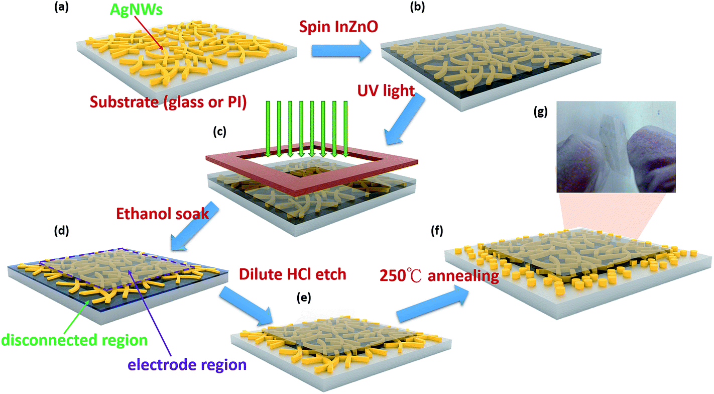 | ||
| Fig. 1 A schematic of the fabrication process of the DUV-lamp-writing AgNW pattern with an IZO capping layer. | ||
For application demonstration, we fabricated an organic photodetector (OPD) using the proposed DUV-patterned AgNW electrode as the bottom electrode. We first prepared the ZnO-capped AgNW electrode with a line width of about 150 μm. Next, a 400 nm-thick organic layer was formed via blade coating a mixture of poly{[4,8-bis-(2-ethyl-hexyl-thiophene-5-yl)-benzo[1,2-b:4,5-b′]dithiophene-2,6-diyl]-alt-[2-(2′-ethyl-hexanoyl)-thieno[3,4-b]thiophen-4,6-diyl]} (PBDTTT-C-T) and [6,6]-phenyl-C61-butyric acid methyl ester (PCBM) with a weight ratio of 2:3 and with a total 2.6 wt% dissolved in chlorobenzene (CB). Finally, the top electrode was formed by dropcasting the AgNWs (0.125 wt% in IPA). The OPD was then measured using white light (7000 lux on the sample surface) that irradiated the sample from both the topside and bottom side.
3. Results and discussion
Initially, we compared the thermal stabilities of bare AgNWs and the IZO-capped AgNWs. The scanning electron microscopy (SEM) images of AgNWs and IZO-capped AgNWs prepared at different annealing temperatures were compared and are shown in Fig. 2. The annealing time was fixed at 1 hour. The SEM images obtained before thermal annealing are also shown. We clearly observed that when the annealing temperature was 200 °C, the AgNWs started to have broken melted lines. When the temperature was 250 °C, the AgNWs even melted to be the Ag dots. On the contrary, with the IZO capping, the AgNW network was well retained even when the annealing temperature was as high as 300 °C. The sheet resistances of the AgNWs and the IZO-capped AgNWs are plotted as a function of annealing temperature (from 25 °C to 300 °C) in Fig. 3. The data are the average value obtained via measuring three different positions on the samples. The deviation was lower than 1%, which was too small to be observed in Fig. 3. When compared with the sheet resistance of 7 ohm per square for the samples obtained without any thermal annealing, the sheet resistance of the IZO-capped AgNWs (the red dot symbols) slightly increased to 8 ohm per square after thermal annealing at 250 °C or 300 °C. This slight increase is considered to be acceptable in most of the applications. If there is no IZO capping, the sheet resistance of the bare AgNWs (the black square symbols) drastically increases when the thermal annealing temperature is higher than 200 °C. In summary, the proposed sol–gel IZO capping process is an effective and low-cost method to greatly improve the thermal stability of the AgNWs. Note that in addition to IZO, ZnO can also be used to cap the AgNWs to improve their thermal stability. As shown by the blue star symbols in Fig. 3, conductive ZnO/AgNW electrodes were successfully demonstrated at both 25 °C and 250 °C. The transmittance for the IZO/AgNWs or ZnO/AgNWs was about 70–80% in the visible-light range (not shown). | ||
| Fig. 2 The SEM images of bare AgNWs and the IZO-capped AgNWs with 1 h of thermal annealing at different temperatures. | ||
 | ||
| Fig. 3 The sheet resistances of bare AgNWs and the IZO-capped AgNWs plotted as a function of annealing temperature. Data for the ZnO-capped AgNWs are also shown (blue star symbols). | ||
In addition to improving the thermal stability, the results, as shown in Fig. 3, can be used to pattern the AgNWs. It has been reported that a DUV lamp can induce the M–O–M condensation reaction in sol–gel oxide precursors.20,21 As a result, sol–gel oxide materials, such as indium–gallium–zinc oxide (IGZO), can be self-patterned upon irradiating DUV light through a mask. Herein, as shown in Fig. 3, we observed that thermal annealing at 250 °C broke the connections between bare AgNW, but did not affect the high conductivity of the IZO-capped AgNWs. We then attempted to pattern the sol–gel IZO on top of the AgNWs by irradiating the DUV lamp through a mask, as shown in Fig. 1(c). The non-irradiated IZO will be removed by ethanol (Fig. 1(d)), and the bare AgNWs will be exposed. Then, ideally, via thermal annealing at 250 °C, the uncovered bare AgNWs will be fully melted to form a disconnected region. On the other hand, the IZO-capped AgNWs retain their original network to serve as the electrode region. However, when we observed the SEM images of the proposed electrode region and the disconnected region, as shown in Fig. 4(a), we found that the AgNWs in the disconnected region still retained a rather good network. No significant AgNW melting phenomenon was observed. We, then, speculated that even after ethanol dipping, there might be a thin IZO residue layer remaining on top of the AgNWs. To remove the residual IZO thin film, we placed the whole sample in dilute hydrochloric acid (HCl) to slightly etch the whole IZO film. By suitably controlling the HCl concentration and the etching time, we can successfully retain the IZO film in the electrode region and completely remove the very thin IZO film in the disconnected region. The resulting results can be observed in the SEM images shown in Fig. 4(b). After being dipped in dilute HCl, the AgNWs in the disconnected region melt to become Ag nanodots at 250 °C. The influence of HCl etching was further investigated by comparing the sheet resistance in the disconnected region and in the electrode region while changing the HCl etching time from 0 (original), 5, 10, 15, to 20 s (Fig. 5). In the disconnected region, when the etching time was higher than 15 s, the IZO residue was completely removed to obtain a high resistivity. However, longer etching time cannot be applied to remove the IZO in the electrode region. As shown in Fig. 5, an etching time longer than 20 s will cause a 3-time increase in the sheet resistance in the electrode region. We, hence, chose an etching time of 15 s in the following work. For the samples on a PI substrate, we also marked the sheet resistances of the disconnected region and electrode region using red star symbols, as shown in Fig. 5. The proposed method can generate a 6-order conductivity difference between the disconnected region and the electrode region.
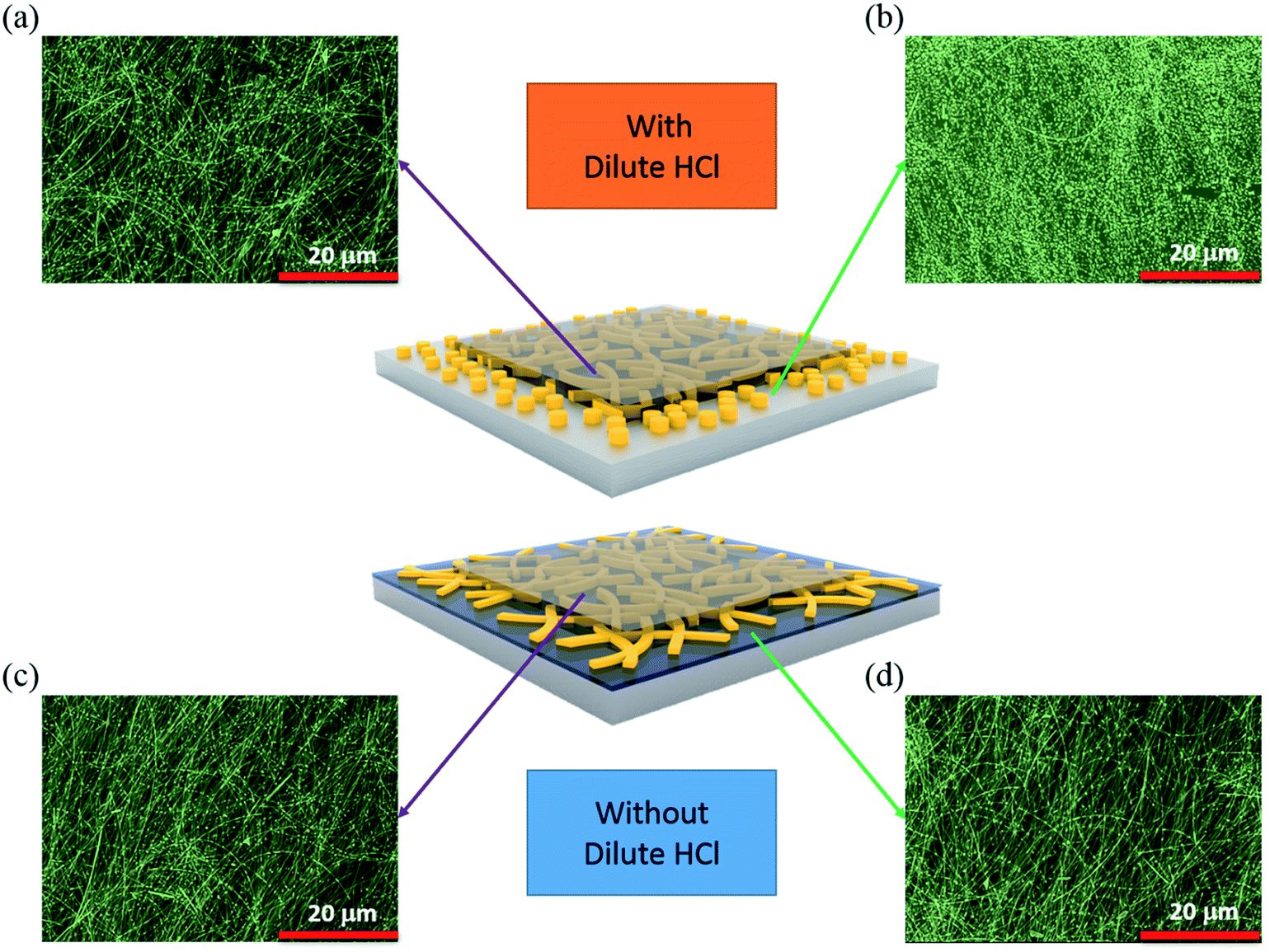 | ||
| Fig. 4 A schematic of the DUV-patterned IZO-capped AgNWs with and without dilute HCl etching. The (a) and (c) SEM images of the electrode regions and (b) and (d) SEM images of the disconnected regions. | ||
 | ||
| Fig. 5 The sheet resistances of the electrode regions and the disconnected regions (on a glass substrate) with dilute HCl etching at different etching times. The red star symbols represent the data obtained using a PI substrate. | ||
After determining the optimal HCl etching time, we then fabricated patterned AgNW electrodes on glass and PI substrates. As shown in Fig. 6, the schematic shows the AgNW pattern including a 100 μm-wide disconnected region between two AgNW electrode regions. The corresponding SEM images are also provided. We successfully formed the AgNW pattern and the width between two electrode regions was about 90 μm and 110 μm when the substrate was glass or PI, respectively. The resolution may be further improved in future work by reducing the distance between the mask and the substrate. For sensor or photovoltaic applications, the 100 μm critical dimension is acceptable. When compared with the screen-printed AgNW pattern,21,24 an improved resolution was obtained via the proposed method. When compared with the inkjet-printed AgNWs,23,24 our method has a comparable resolution and a potentially improved throughput for large-area processing since the DUV lamp irradiation can be easily scaled up. The electrical properties of the AgNW pattern produced are also shown in Fig. 7. For the AgNW pattern on a glass substrate, very high current (reaching the current limit of the measurement system) was obtained when the two probes were used to measure the current–voltage (I–V) characteristics in the electrode region (Fig. 7(a)), revealing the very good connecting properties of the AgNWs. On separately probing the two electrode regions, the leakage current through the disconnected region was found to be lower than 5 pA, as shown in Fig. 7(b). The very low leakage current verifies the feasibility of the proposed patterning method. Then, we investigated the connecting properties and the leakage current of the AgNW patterns on the PI substrate, as shown in Fig. 7(c) and (d), respectively. The initial I–V curve and the I–V curve after 1000-time bending are shown. It was confirmed that the proposed AgNW patterning method could be used on a plastic substrate to form bendable transparent electrodes.
 | ||
| Fig. 6 A schematic to show the disconnected line between two electrode regions. The corresponding SEM images on glass and PI substrates are also shown. | ||
 | ||
| Fig. 7 The current–voltage curves obtained for the proposed IZO/AgNW electrode patterns on a glass substrate when (a) probing inside one electrode region and (b) probing two electrode regions separated by a 100 μm-wide disconnected region. The current–voltage curve obtained for the proposed IZO/AgNW patterns on a PI substrate when (c) probing inside one electrode region and (d) probing two electrode regions separated by a 100 μm-wide disconnected region. In (c) and (d), the I–V curves before bending and after 1000 times bending are both plotted. | ||
Finally, to demonstrate a possible application, we fabricated an organic photodetector using the proposed DUV-patterned AgNW electrode as the bottom electrode. The DUV-patterned ZnO-capped AgNW electrode was used because it could deliver good conductivity like the IZO-capped AgNW electrode (Fig. 3). As shown in Fig. 8(a), we firstly prepared the ZnO-capped AgNW electrode with a linewidth of about 150 μm. Next, a 400 nm-thick organic PBDTTT-CT/PCBM layer was coated (Fig. 8(b)). Finally, as shown in Fig. 8(c), a top electrode was formed by dropcasting the AgNWs. The details of the process are given in the Experimental section. The image of the DUV-patterned ZnO/AgNWs is shown in Fig. 8(d). We can see a very light T-shape pattern, indicating the transparent electrode. The current–voltage characteristics of the OPD are shown in Fig. 8(e). When white light was irradiated from the topside or from bottom side, the photocurrents were about 2 orders higher than the dark current. This result verifies that the proposed DUV-patterned electrode can really be used in an optoelectrical device to serve as a conductive and transparent electrode.
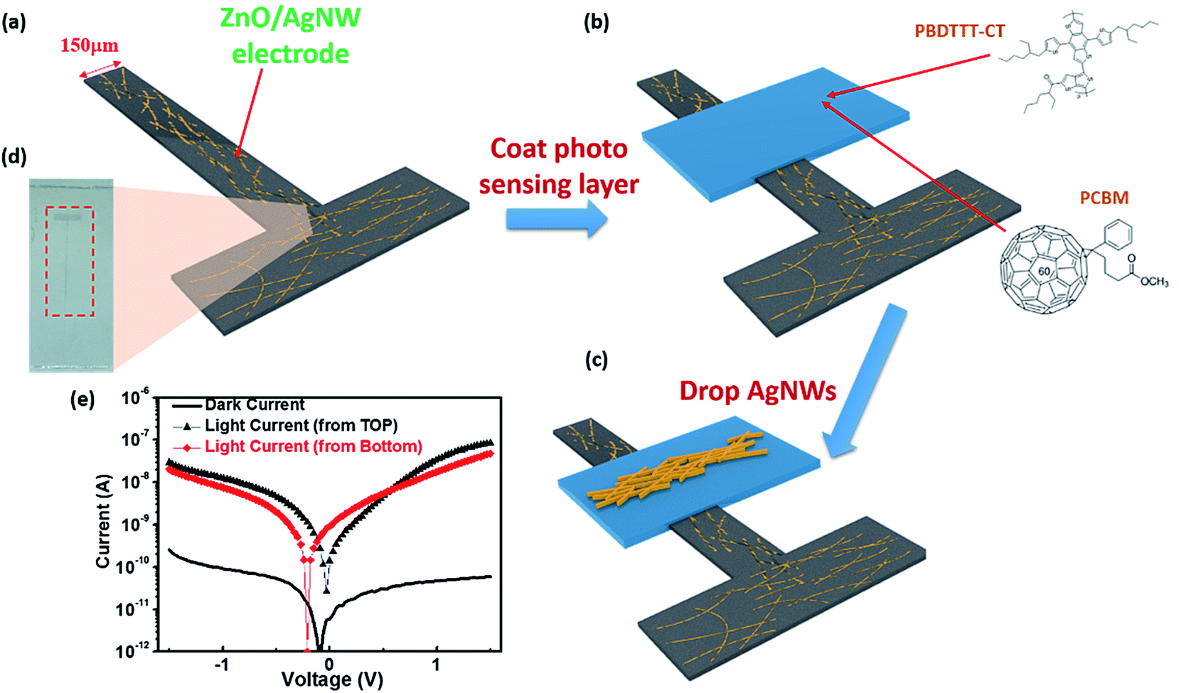 | ||
| Fig. 8 (a–c) A schematic of the fabrication process used to prepare the OPD with ZnO/AgNWs. (d) An image of the DUV-patterned T-shape electrode. (e) The current–voltage characteristics of the OPD with light irradiating from the topside and from the bottom side. | ||
4. Conclusion
We successfully demonstrated a simple DUV lamp irradiation method to pattern a transparent AgNW electrode on a flexible PI substrate with a resolution of 100 μm and 1000-time bending endurance. The pattern was formed using the DUV-activated sol–gel IZO as the capping mask. The IZO-capping can greatly promote the thermal stability of the AgNWs up to 300 °C. On the other hand, at 250 °C, the bare AgNWs melt to become silver dots and become electrically insulating. The DUV-pattern IZO-capping together with the following 250 °C thermal annealing is effective to form AgNW patterns on flexible PI substrates. The proposed low-cost method is promising for developing AgNWs on large flexible substrates for sensor or photovoltaic applications. Note that the capping material was not limited to IZO, and DUV-patterned ZnO-capped AgNWs were also successfully demonstrated to exhibit acceptable transparency and conductivity.Acknowledgements
This work was supported by Ministry of Science and Technology, Taiwan (number 104-2923-E-009-001-MY3) and Agence Nationale de la Recherche, France (PHOTOMOC program, No. N ANR-14-CE26-0039-01). The authors, Yi Zhang and Bo-Ru Yang, would like to acknowledge the financial support from Science and Technology Project of Guangdong Province (number 2015B090915003) for the study on high-temperature PI substrate.Note and references
- B. Sciacca, J. van de Groep, A. Polman and E. C. Garnett, Adv. Mater., 2016, 28, 905–909 CrossRef CAS PubMed.
- P. H. Wang, S. P. Chen, C. H. Su and Y. C. Liao, RSC Adv., 2015, 5, 98412–98418 RSC.
- B. C. Feng, K. Liu, J. S. Wu, L. Liu, J. S. Cheng, Y. Zhang, Y. Sun, Q. Li, S. Fan and K. Jiang, Adv. Funct. Mater., 2010, 20, 885–891 CrossRef.
- Z. Li, S. A. Kulkarni, P. P. Boix, E. Shi, A. Cao, K. Fu, S. K. Batabyal, J. Zhang, Q. Xiong, L. H. Wong, N. Mathews and S. G. Mhaisalkar, ACS Nano, 2014, 8, 6797–6804 CrossRef CAS PubMed.
- Y. H. Shin, C. K. Cho and H. K. Kim, Thin Solid Films, 2013, 548, 641–645 CrossRef CAS.
- T. He, A. Xie, D. H. Reneker and Y. Zhu, ACS Nano, 2014, 8, 4782–4789 CrossRef CAS PubMed.
- B. R. Yang, W. Cao, G. S. Liu, H. J. Chen, Y. Y. Noh, T. Minari, H. C. Hsiao, C. Y. Lee, H. P. D. Shieh and C. Liu, ACS Appl. Mater. Interfaces, 2015, 7, 21433–21441 CAS.
- A. R. Madaria, A. Kumar, F. N. Ishikawa and C. Zhou, Nano Res., 2010, 3, 564–573 CrossRef CAS.
- G. S. Liu, C. Liu, H. J. Chen, W. Cao, J. S. Qiu, H. P. D. Shiehc and B. R. Yang, Nanoscale, 2016, 8, 5507 RSC.
- A. R. Madaria, A. Kumar and C. Zhou, Nanotechnology, 2011, 22, 245201 CrossRef PubMed.
- D. Chen, J. Liang, C. Liu, G. Saldanha, F. Zhao, K. Tong, J. Liu and Q. Pei, Adv. Funct. Mater., 2015, 25, 7512–7520 CrossRef.
- Q. Xu, W. Shen, Q. Huang, Y. Yang, R. Tan, K. Zhu, N. Daic and W. Song, J. Mater. Chem. C, 2014, 2, 3750–3755 RSC.
- T. B. Song, Y. S. Rim, F. Liu, B. Bob, S. Ye, Y. T. Hsieh and Y. Yang, ACS Appl. Mater. Interfaces, 2015, 7, 24601–24607 CAS.
- S. B. Yang, H. K. Choi, D. S. Lee, C. G. Choi, S. Y. Choi and I. D. Kimsmall, Small, 2015, 11, 1293–1300 CrossRef CAS PubMed.
- Y. Park, L. Bormann, L. M. Meskamp, K. Vandewal and K. Leo, Org. Electron., 2016, 36, 68–72 CrossRef CAS.
- X. Yan, J. Ma, H. Xu, C. Wang and Y. Liu, J. Phys. D: Appl. Phys., 2016, 49, 325103 CrossRef.
- D. Lee, H. Lee, Y. Ahn and Y. Lee, Carbon, 2015, 81, 439–446 CrossRef CAS.
- M. Göbelt, R. Keding, S. W. Schmitta, B. Hoffmann, S. Jäckle, M. Latzel, V. V. Radmilović, V. R. Radmilović, E. Spiecker and S. Christiansen, Nano Energy, 2015, 16, 196–206 CrossRef.
- Y. Ahn, Y. Jeong and Y. Lee, ACS Appl. Mater. Interfaces, 2012, 4, 6410–6414 CAS.
- H. C. Lin, F. Stehlin, O. Soppera, H. W. Zan, C. H. Li, F. Wieder, A. Ponche, D. Berling, B. H. Yeh and K. H. Wang, Sci. Rep., 2015, 5, 10490 CrossRef PubMed.
- S. Yao and Y. Zhu, Nanoscale, 2014, 6, 2345–2352 RSC.
- Y. S. Rim, H. Chen, Y. Liu, S. H. Bae, H. J. Kim and Y. Yang, ACS Nano, 2014, 8, 9680–9686 CrossRef CAS PubMed.
- D. J. Finn, M. Lotya and J. N. Coleman, ACS Appl. Mater. Interfaces, 2015, 7, 9254–9261 CAS.
- J. Liang, K. Tong and Q. Pei, Adv. Mater., 2016, 28, 5986–5996 CrossRef CAS PubMed.
- L. Yang, T. Zhang, H. Zhou, S. C. Price, B. J. Wiley and W. You, ACS Appl. Mater. Interfaces, 2011, 3, 4075–4084 CAS.
- M. Amjadi, A. Pichitpajongkit, S. Lee, S. Ryu and I. Park, ACS Nano, 2014, 8, 5154–5163 CrossRef CAS PubMed.
| This journal is © The Royal Society of Chemistry 2017 |