
 Open Access Article
 This Open Access Article is licensed under a
 Creative Commons Attribution 3.0 Unported Licence
Scanning tunneling spectroscopic monitoring of surface states role on water passivation of InGaAs uncapped quantum dots†
M. J. Milla *a,
I. Hernández-Rodríguezb,
J. Méndezb,
Jorge M. Garcíac,
J. M. Ulloaa and
Á. Guzmána
*a,
I. Hernández-Rodríguezb,
J. Méndezb,
Jorge M. Garcíac,
J. M. Ulloaa and
Á. Guzmána
aInstituto de Sistemas Optoelectrónicos y Microtecnología (ISOM), Madrid, Spain. E-mail: mjmilla@die.upm.es
bInstituto de Ciencia de Materiales de Madrid (ICMM-CSIC), Spain
cMBE Lab, IMM-Instituto de Microelectrónica de Madrid (CNM-CSIC), Spain
First published on 29th June 2017
Abstract
A detailed local analysis of the impact of water coverage on the density of surface states in In0.5Ga0.5As surface nanostructures is reported by spectroscopy monitoring the surface conductivity at the nanometer-scale. A correlation between the changes of the surface conductivity and the variation of the density of surface states under different environmental conditions is found in terms of I–V characteristics and scanning tunneling spectroscopy. From dry to humid conditions the surface conductivity of a three-dimensional In0.5Ga0.5As uncapped nanostructured surface increases monotonically with the reduction of the density of available surface states. In contrast, neither the electrical properties nor the density of electrically active surface states of a surface quantum well exhibit any significant dependence on the external moist conditions. The adsorption of water molecules onto the surface passivates the surface states leading to an improvement in the electron transport. These results clearly reveal that the density of surface states depends on the dimensionality of a nanostructured surface and demonstrate the important role of these states for nanoengineering sensing devices.
Introduction
Surface states, arising from the termination of a bulk crystal, are key characteristics of semiconductor surfaces. Such states give rise to spatially located electronic states within the midgap. These localized states are suggested to act as nonradioactive recombination and trapping centers playing a critical role on the determination of the macroscopic property changes related to variations in the environment.1 Recently, changes in the piezoelectric signal, surface conductivity and photoluminescence with different surrounding conditions have been reported for different surface semiconductors such as ZnO nanowires,2 graphene,3 carbon quantum dots (QDs)4 and III–V surface QDs (SQDs).1,5–10 This high reactivity to environmental agents makes surface solid state semiconductors well-suited materials for the development of sensing applications. The presence of a nanostructured surface, characterized by the existence of surface states and strain relaxation, provides an exceptional tool to nanoengineer sensing devices.Qualitative interpretations based on surface states passivation have been proposed as the main physical phenomena to such environmental response. The effect of changing the density of surface states at the atomic scale directly influences the macroscopic physical properties. However, the evolution of such localized states is not evident yet. Local techniques generally based on scanning probe microscopy (SPM) systems are usually employed for surface characterization.11,12 Particularly, scanning tunneling microscopy and spectroscopy (respectively STM and STS) are excellent techniques for such purpose. In particular, STS allows probing local electronic properties down to the atomic scale.13,14
In this work, we address the role of surface states on the physical properties of surface III–V semiconductor nanostructures by spectroscopically monitoring their electrical response under different water vapor concentration. We compare the electrical and spectroscopic response to moist conditions of the same material (In0.5Ga0.5As) engineered into surface quantum well (SQW) and SQD. The conductivity of the samples as a function of the external humidity is measured both in a macroscopic and a nanoscopic scale. Macroscopic conductivity is examined evaluating the current–voltage (I–V) characteristics under different air humidity conditions. The local conductivity properties are determined by STS measurements varying the water coverage of the sample. We report a significant change in the local I–V response of SQD compared to that of SQW, which is attributed to passivation of active surface states.
Materials and methods
Two samples are compared to demonstrate the differences on their surface states density and thus, their dissimilar response to external conditions. One sample contains an unburied In0.5Ga0.5As QD layer and the other sample consists of a surface In0.5Ga0.5As QW. The samples were grown in a RIBER-32 solid-source molecular beam epitaxy (MBE) on a n-doped GaAs(100) substrate. Following the oxide desorption, a 1.5 μm GaAs buffer layer was grown at 590 °C and 1 ML per s. Then, an uncapped In0.5Ga0.5As QW or QD layer was grown at low temperature (430 °C) and slow growth rate (0.07 ML per s). The amount of deposited material was 2.8 ML (below the critical thickness, 4.4 ML) in the case of the SQW and 6 ML for the SQD. The QD layer was formed by the Stranski–Krastanov method. In situ reflection high-energy electron diffraction (RHEED) was used to monitor the growth.The In0.5Ga0.5As surface nanostructures were structurally characterized by atomic force microscopy (AFM) in tapping mode using diamond-coated Si tips. Fig. 1 shows a histogram of the nanostructure height in a 1 μm2 area of the AFM images for the SQD and SQW (insets (a) and (b) respectively). The counts do not correspond to the number of QDs since the step used to scan the surface is much smaller than the QD diameter. SQW sample presents a nearly flat surface, with a maximum height and mean roughness of 0.9 nm and 0.3 nm, respectively. Nonetheless, the SQD sample exhibits an ensemble of nanostructures showing a high degree of homogeneity and a large density (7.1 × 1010 cm−2) with an average height of 6.1 ± 0.2 nm and lateral diameter of 34 ± 2 nm.
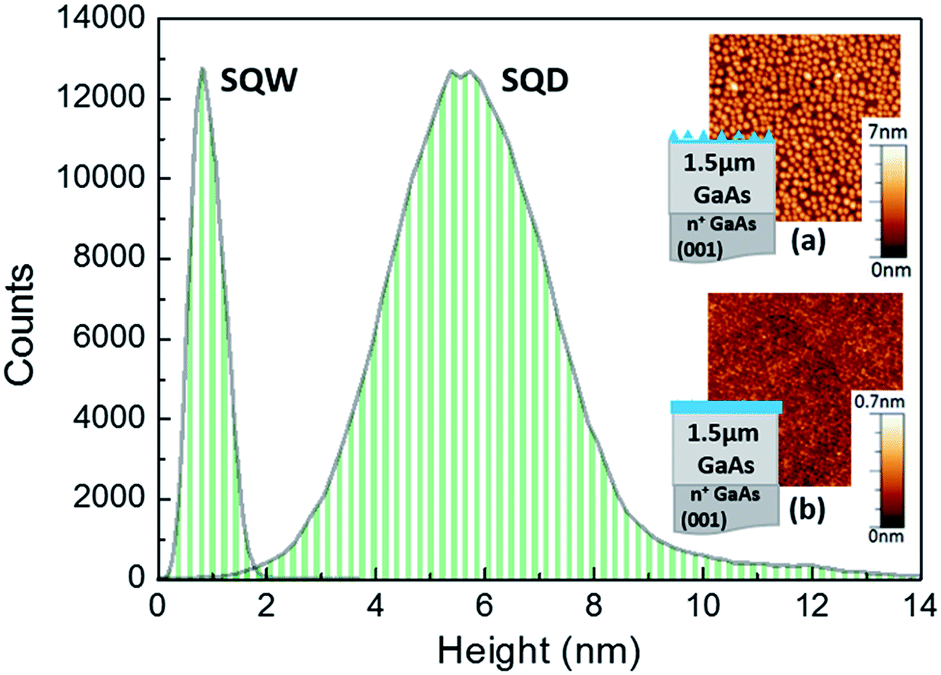 | ||
| Fig. 1 Histogram of the height in a 1 μm2 area of the AFM images for the SQD and SQW (a) SQD sample exhibits a high degree of homogeneity and a large surface density (7.1 × 1010 cm−2), and they have on average a 6.1 ± 0.2 nm height and a 34 ± 2 nm lateral diameter (b) SQW sample presents a nearly flat surface, with a maximum height and mean roughness of 0.9 nm and 0.3 nm, respectively. | ||
Concerning the electrical characterization, we performed I–V measurements using a semiconductor parameter analyzer (HP4145). Two 150 μm-side Ti/Au metal contacts of (10/130 nm) were deposited on the surface of the sample separated by 70 μm. These contacts were not annealed to avoid metal diffusion into the bulk and thus, to ensure the conduction through the surface. A macroscopic surface differential conductivity was obtained from the derivative of the I–V characteristics measured between those contacts. The samples were placed in an opaque and hermetically sealed box especially designed for such analysis.15 The electrical measurements were carried out at a temperature of 24 °C, under light conditions to ensure the presence of photoexcited electron–hole pairs8 (source: blue LED, ∼2.7 eV, at 7.4 μW) and under different relative humidity (RH) conditions from 0% to 70%.
Nanoscopic studies were carried out using an Omicron VT-STM microscope in an Ultra-High Vacuum chamber with a base pressure of 1 × 10⁻¹⁰ mbar and using control electronics and software from NANOTEC.16 Tungsten tips were used after in situ cleaning and re-sharpening treatments.17 Spectroscopic measurements were performed by acquiring I–V plots over micrometer-size regions and extracting averages from homogeneous areas. In the STM configuration the contact to the sample is through tantalum wires that press the sample against the sample-holder. Therefore the measured conduction is the tunneling from the tip to the sample just under the tip, plus the surface conduction (parallel to the plane) from that point until the contact to the tantalum wire, and then the conduction through the contact. The main difference between the macroscopic and nanoscopic measurements is that in the macroscopic experiments there are two contacts and in the STM configuration one contact and the tunneling junction. Surface conduction is therefore present in both scenarios. Special attention was paid18 to avoid artifacts related to strong tip–surface interactions during the STS. The surface density of states (DOS) was calculated from the normalized derivative of the I–V characteristics,19 while the conductance was obtained from the slope at the origin.
Results and discussion
At negative bias voltage applied to the tip, the normalized derivative corresponds to the density of empty surface states (Fig. 2(a)). The sample under study is exposed to water obtained from a deoxygenized pure water crucible. The pressure of the chamber rises to 5 × 10⁻⁸ mbar during the exposure.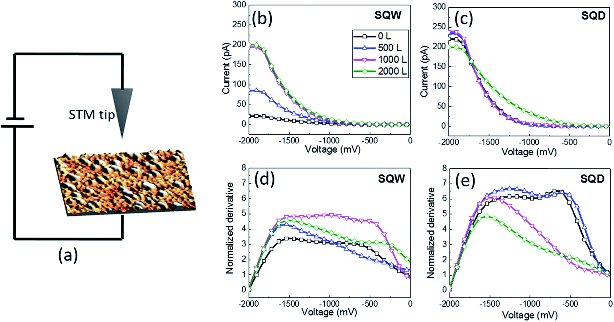 | ||
| Fig. 2 (a) Scheme of the STM/STS measurements. (b), (c) I–V plots and (d), (e) normalized derivative (density of states) obtained for SQW and SQD for different water dose (in Langmuir). A negative bias was applied to the tip, consequently the normalized derivative shown in (d) and (e) correspond to the density of empty surface states. | ||
The STS I–V characteristics are performed in an array of 512 × 512 points within the acquired micron-sized STM image. An average of STS spectra is performed over areas in order to enhance the signal-to-noise ratio (see Section A in the ESI†). Fig. 2(b) and (c) present the I–V curves obtained for SQW and SQD samples respectively and their evolution when increasing the exposure to water. The tunneling current concerns the contribution of both: the states of the nanostructure itself and the surface states.20 All the I–V measurements show a rectifying behavior with predominant conduction at negative bias (respect to the tip), associated with injection of electrons into the empty states of the sample. For this reason it is represented only the negative axis of the plot. The water dose is calculated from the water pressure (5 × 10⁻⁸ mbar) and the exposure time using the Langmuir definition, i.e., one monolayer (1 ML) is adsorbed in 1 second at a pressure of 10−6 mbar, assuming a sticking coefficient of 1. Several water doses up to 2000 L were tested (Fig. 2). The conductance of the In0.5Ga0.5As SQD (measured as the derivative at zero) exhibits a continuous increase with the water dose, reaching a metallic-like behavior at 2000 L. Normalized derivatives19 (proportional to the density of surface states) of SQW and SQD are addressed in Fig. 2(d) and (e) respectively for the different water dose (see Fig. S-2, in the ESI†). No clear tendency for the SQW sample is observed. In contrast, the SQD sample exhibits a reduction of the density of states with water adsorption. Considering the Fig. 2(e) for 0 L and 500 L two peaks can be observed, at approximately −600 mV and −1300 mV. Increasing the water exposure from 1000 L to 2000 L the first peak almost disappears and the second has a reduction together with a slight shift to higher voltage values. According to these results, the contribution of the states of the nanostructure to the tunneling current is weaker than that coming from the passivation of surface states. Without water, it is shown already a tunneling current different to zero, so that, even if there are unoccupied surfaces states acting as trapping centers, they do not completely prevent tunneling. However, when increasing the water coverage we observe a clear increase in the tunneling current, attributed to the occupation of the surface states and then the ease flow of carriers. The fact that current is strongly affected by the environment points to a dominant role of surface states, since the effect of environment on QD levels should in principle be much weaker. Besides, this correlates with the density of states, calculated as the integral of these plots, has a clear decrease with water dose.
The evolution of the density of states can be observed in Fig. 3(a) and (b) where we have represented the density of states for sixteen different spectroscopic images taken in the SQD (blue squares) and SQW (red circles) samples for each water dose. The average values are plotted as solid black squares in the case of SQD and as solid black circles in the case of SQW, together with the dispersion error bars. Two different states in the spectra of the density of surface states in the case of SQDs can be recognized. One of them affected by the water level and the other unaffected. Under dry conditions, the SQD sample presents a higher density of empty surface states than the SQW sample. Upon water exposure, two different behaviors can be observed for SQD and SQW samples when varying the water pressure in the chamber. On one hand, the SQW sample shows a small change of the density of surface states with water adsorption. On the other hand, the density of surface states of the SQD sample decays when the water coverage is increased. These spectroscopic data are sensitive to local variations of conductivity in a surface partially covered with water, which explains the high dispersion of the experimental points in some cases. For example, at 2000 L (see Fig. 3(a)), a dispersion of the density of states is viewed, showing the partially surface coverage with water. The higher values corresponds to local areas where the QDs are clearly resolved (approx. 6 a.u.), and the lower density of states (approx. 3 a.u.) corresponding to fully water covered areas, where the QDs are not visible as it can be observed in Fig. 3(c). In Fig. 3(d) we show a spectroscopic image obtained from the normalized derivative at each point and extracting the value of the density of states at −1.5 V. It is clearly observed how the water covered areas present a decrease in the density of states, viewed as darker areas in the image. Finally, at 2000 L and furthermore time after closing the water valve (Section B in the ESI†) the data dispersion is reduced, and we measure low density of states together with STM images presenting no features at all. This reduction of the dispersion points out to be an effect of the water diffusion, but also part of it could came from the STM tip, as it produces a shadow effect to the water adsorption or sweeping out the water from the scanning region.
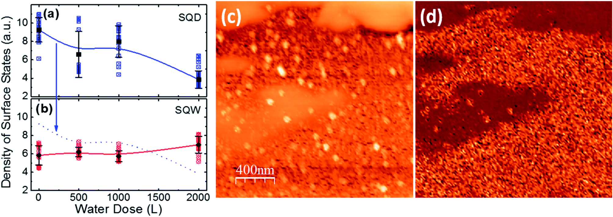 | ||
| Fig. 3 Variation of the density of unoccupied surface states as a function of the water dose in Langmuir (L) of (a) SQD and (b) SQW sample. Solid lines are a plotted as a guide to the eye. The guide to the eye of SQD results is plotted also in (b) as a dotted line for comparison. Increasing the water dose yields to a reduction of the density of surface states in SQD sample, in contrast, they remain nearly constant in the SQW sample. (c) Topography of the SQD sample. STM image corresponding to an area partially covered with water molecules. (d) Spectroscopic image obtained simultaneously with (c) and extracted from the normalized derivative at −1.5 V. | ||
A comparison of the macroscopic and nanoscopic response when exposing the two samples to different water containing atmospheres is illustrated in Fig. 4. The surface conductivity of SQW and SQD samples obtained from I–V characteristics measured between contacts is shown in Fig. 4(a). The values was recorded at V = −1.5 V as a function of the RH in the environment from 0% to 70% in steps of 10% RH. According to these findings, once more, a high importance of the surface morphology on the electrical response can be inferred. The SQW sample does not exhibit any noticeable variation when increasing the RH in the surrounding. Conversely, the SC of the SQD sample gradually rises with RH. From 0% to 70% of RH, SC exhibits an increment of about 85 times compared to dry conditions. Fig. 4(b) illustrates the local conductivity of the SQW and SQD samples measured by STS, as a function of the water coverage in Langmuir (L). Parallel to the macroscopic result, the SQW sample shows a small variation of the SC with increasing the water dose, while the SC of the SQD clearly rises with water adsorption. This enhancement is particularly prominent for a water coverage of 500 L.
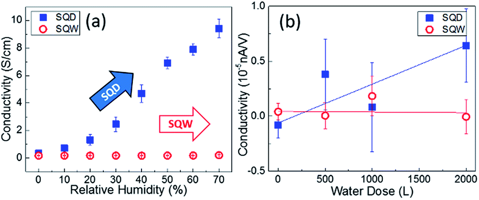 | ||
| Fig. 4 Comparison of the macro and nanoscopic conductivity for different moist conditions. (a) Variation of the surface conductivity of SQW and SQD samples measured between contacts at −1.5 V as a function of the RH in the environment. (b) Variation of the local conductivity with the water dose as measured by STS. | ||
The higher surface-to-volume ratio of the SQD sample compared to that of the SQW sample, along with the higher surface complexity of the former sample lead to a larger density of surface states and thus, to a higher surface sensitivity. Increasing the RH in the environment enhances the partial pressure of water vapor surrounding the sample and thus, the probability of water adsorption onto the surface.
The adsorption of water molecules onto the surface may alter the physical properties of the surface. In fact, the impact of such physisorption process on the optical and electrical properties has been recently reported, attributing the improvement to the surface passivation7,15,21–23 or oxidation24 and therefore, to the reduction of the density of active surface states after water adhesion. Passivation and oxidation are two processes that take place on the surface and may alter the physical properties of the surface nanostructures. The former refers to the filling of the surface states decreasing the density of active centers, thus making less sensitive the surface to external change and consequently, improving the physical properties. Although leading to the same result, the second does not consider the mentioned surface states but a formation of a thin oxide layer (apart from the native oxide) that prevents changes arising from external interactions. The main difference of the two process is the reversibility: passivation is a reversible process whereas oxidation is non-reversible.25 In our case, we have already reported that the changes shown in the physical properties (i.e. photoluminescence at room temperature and surface conductivity) of the InGaAs nanostructures are reversible, meaning that after a certain time or vacuum treatment, the sample recovers the initial as-grown characteristics.7,8 Therefore, we can assume as more likely the passivation process to be the main responsible for the surface reactivity of our system. The reactivity shown by surface semiconductor nanostructures enables the selective adsorption of the molecules in the surroundings.26 Such states stem from different events taking place at the surface during surface formation, including, among others, relaxation and reconstruction processes, unsaturated bonds, crystal discontinuities and imperfections. The characteristics of these localized states depend not only on the material composition but also on the crystallographic orientation and surface dimensionality.21,27 In 1998, Saito et al. reported the existence of surface states within the midgap for InAs SQDs by using theoretical calculations based on the Keating potential for the strain calculations.28 Besides, it has been also shown that the nature and the density of such localized states change with the external conditions. The position of such surface states within the bandgap depends on the material itself and on the environment. So that, surface states can be acceptor- or donor-like and the net configuration into a system may alternate into more donor-like or acceptor-like from as-grown to treated sample, respectively.28,29 Indeed, oxidation process has been found to influence in the nature of the surface states, causing a transition from donor to acceptor-like states and vice versa.24
Our local spectroscopic results show that the surface states in the InGaAs surface nanostructures are observed when tunneling into the empty states, and as a consequence, we can infer that such traced states behave as acceptor-like. Besides, no energy shift in the photoluminescence at room temperature is observed when changing the environment,26 thus indicating no change in the nature of the localized states from donor- to acceptor-like.24 Consequently, passivation can be considered as the main process affecting our nanostructures. Therefore, assuming passivation and acceptor-like states, one can consider that, initially, the surface states are empty and in the proximity to water molecules, they attract such molecules to the surface. Water molecules, defined as donor molecules,30 are finally adsorbed into the surface, passivating the non-radiative active centers and improving the optical and electrical properties. Besides, STS findings reveal that in fact, the density of surface states depends on the surface morphology since under dry conditions the density of surface states of a SQD sample is larger than that of SQW. Furthermore, regarding the nature of the surface dimensionality, these results also portray a different evolution tendency of the density of the surface states with the external conditions. SQD sample exhibit a significant decay of the density of the surface states when increasing the water coverage. On the contrary, the density of surface states in the SQW sample remains nearly unchangeable even at high water pressure in the chamber. This matches well with the results obtained for the electrical results. In the case of the SQD sample, when enhancing the amount of water molecules in the surrounding the adsorption process turns more likely, passivating the surface states and therefore reducing the number of available states as found from the STS measurements, resulting in an increase of the SC. Moreover, the negligible variation of the SC in the case of the SQW sample is tightly related to the unchangeable density of surface states obtained from the local analysis.
Conclusions
In conclusion, we conducted a nanoscopic and macroscopic comparison of the electrical response of an In0.5Ga0.5As SQW and an In0.5Ga0.5As SQD under different humidity conditions. The results highlight the importance of the surface morphology and the variation of the density of surface states for sensing applications. The SQW sample does not exhibit any noticeable SC change when increasing the moisture in the atmosphere; whereas the SC of the SQD sample shows an increase of more than one order of magnitude when changing the RH from 0% to 70%. The STS analysis shows a perfect correlation with the SC findings. Considering an increment of the water pressure in the chamber above 500 L, a negligible variation of the density of surface states was found in the case of SQW sample compared to that shown by the SQD sample. Assuming acceptor-like states, the density of surface states of SQD gradually decays when enhancing the water coverage pointing to the adsorption of water molecules as the main drive force for the passivation process and thus, for such exceptional properties. These results clearly demonstrate the effect of the surface states on the sensitivity of the sample to environmental changes and the great suitability of In0.5Ga0.5As SQD nanostructures for the development of humidity sensor devices.Acknowledgements
This work has been supported by the following projects: MAT2011-26534, MAT2014-54231-C4-1-P, AIC-B-2011-0806, MAT2015-67021-R.Notes and references
- J. Moison, K. Elcess, F. Houzay, J. Marzin, J. Gérard, F. Barthe and M. Bensoussan, Phys. Rev. B: Condens. Matter Mater. Phys., 1990, 41, 12945–12948 CrossRef CAS.
- X. Xue, Y. Nie, B. He, L. Xing, Y. Zhang and Z. L. Wang, Nanotechnology, 2013, 24, 225501 CrossRef PubMed.
- L. Guo, H.-B. Jiang, R.-Q. Shao, Y.-L. Zhang, S.-Y. Xie, J.-N. Wang, X.-B. Li, F. Jiang, Q.-D. Chen, T. Zhang and H.-B. Sun, Carbon, 2012, 50, 1667–1673 CrossRef CAS.
- X. Zhang, H. Ming, R. Liu, X. Han, Z. Kang, Y. Liu and Y. Zhang, Mater. Res. Bull., 2013, 48, 790–794 CrossRef CAS.
- B. L. Liang, Y. I. Mazur, V. P. Kunets, Z. M. Wang, G. J. Salamo, E. a. DeCuir Jr, B. Passmore and M. O. Manasreh, Nanotechnology, 2008, 19, 65705 CrossRef.
- B. L. Liang, Z. M. Wang, Y. I. Mazur, G. J. Salamo, E. a. DeCuir and M. O. Manasreh, Appl. Phys. Lett., 2006, 89, 43125 CrossRef.
- M. J. Milla, J. M. Ulloa and Á. Guzmán, Appl. Phys. Lett., 2012, 100, 131601 CrossRef.
- M. J. Milla, J. M. Ulloa and Á. Guzmán, ACS Appl. Mater. Interfaces, 2014, 6, 6191–6195 CAS.
- K. Hestroffer, R. Braun, A. Ugur, J. W. Tomm, S. Hackbarth, B. Röder and F. Hatami, J. Appl. Phys., 2013, 114, 163510 CrossRef.
- M. Chen, K. Kobashi, B. Chen, M. Lu and J. M. Tour, Adv. Funct. Mater., 2010, 20, 469–475 CrossRef CAS.
- J. L. Pitters, I. A. Dogel and R. A. Wolkow, ACS Nano, 2011, 5, 1984–1989 CrossRef CAS PubMed.
- W. Melitz, T. Kent, A. C. Kummel, R. Droopad, M. Holland and I. Thayne, J. Chem. Phys., 2012, 136, 154706 CrossRef PubMed.
- R. Weisendanger, Scanning Probe Microscopy and Spectroscopy, Cambridge University Press, Cambridge, 1994 Search PubMed.
- R. M. Feenstra, Surf. Sci., 1994, 299–300, 965–979 CrossRef CAS.
- M. J. Milla, J. M. Ulloa and Á. Guzmán, Nanotechnology, 2014, 25, 445501 CrossRef CAS PubMed.
- I. Horcas, R. Fernández, J. M. Gómez-Rodríguez, J. Colchero, J. Gómez-Herrero and A. M. Baro, Rev. Sci. Instrum., 2007, 78, 13705 CrossRef CAS PubMed.
- N. Nicoara, O. Custance, D. Granados, J. M. García, J. M. Gómez-Rodríguez, A. M. Baró and J. Méndez, J. Phys.: Condens. Matter, 2003, 15, S2619–S2629 CrossRef CAS.
- J. Méndez, J. Gómez-Herrero, J. I. Pascual and A. M. Baró, Appl. Phys. A: Mater. Sci. Process., 1998, 66, S767–S769 CrossRef.
- R. M. Feenstra, J. A. Stroscio and A. P. Fein, Surf. Sci., 1987, 181, 295–306 CrossRef CAS.
- T. K. Johal, R. Rinaldi, A. Passaseo, R. Cingolani, A. Vasanelli, R. Ferreira and G. Bastard, Phys. Rev. B: Condens. Matter Mater. Phys., 2002, 66, 75336 CrossRef.
- Z. Zhang and J. T. Yates, Chem. Rev., 2012, 112, 5520–5551 CrossRef CAS PubMed.
- R. De Angelis, M. Casalboni, F. Hatami, A. Ugur, W. T. Masselink and P. Prosposito, Sens. Actuators, B, 2012, 162, 149–152 CrossRef CAS.
- A. Lin, B. L. Liang, V. G. Dorogan, Y. I. Mazur, G. G. Tarasov, G. J. Salamo and D. L. Huffaker, Nanotechnology, 2013, 24, 75701 CrossRef CAS PubMed.
- G. Trevisi, L. Seravalli and P. Frigeri, Nano Res., 2016, 9, 3018–3026 CrossRef CAS.
- X. Zhang and S. Ptasinska, J. Phys. Chem. C, 2014, 118, 4259–4266 CAS.
- M. J. Milla, J. M. Ulloa and Á. Guzmán, Appl. Phys. Express, 2013, 6, 92002 CrossRef.
- H. Lüth, Solid Surfaces, Interfaces and Thin Films, Springer, Berlin, Heidelberg, 2010 Search PubMed.
- T. Saito, J. N. Schulman and Y. Arakawa, Phys. Rev. B: Condens. Matter Mater. Phys., 1998, 57, 13016–13019 CrossRef CAS.
- E. Halpern, G. Cohen, S. Gross, A. Henning, M. Matok, A. V. Kretinin, H. Shtrikman and Y. Rosenwaks, Phys. Status Solidi A, 2014, 211, 473–482 CrossRef CAS.
- J.-W. Han, B. Kim, N. P. Kobayashi, J. Li and M. Meyyappan, Appl. Phys. Lett., 2012, 101, 142110 CrossRef.
Footnote |
| † Electronic supplementary information (ESI) available. See DOI: 10.1039/c7ra04640e |
| This journal is © The Royal Society of Chemistry 2017 |