DOI:
10.1039/C7RA04330A
(Paper)
RSC Adv., 2017,
7, 29469-29480
Characterization and photoelectrochemical properties of CICS thin films grown via an electrodeposition route
Received
17th April 2017
, Accepted 2nd June 2017
First published on 7th June 2017
Abstract
In this work, cerium doped CuInS2 (CIS) polycrystalline thin films with different Ce content are firstly synthesized on indium doped tin oxide (ITO) glass via a low-cost electrochemical technique. The electrochemical nucleation and growth kinetics of a Cu–In–Ce alloy in a triethanolamine (TEA) plating bath solution onto the ITO glass substrate were investigated by cyclic voltammetry (CV) and chronoamperometry (CA). The composition of CuIn1−xCexS2 (CICS) films was varied by substituting In with Ce with 0 ≤ x ≤ 0.15 (x = Ce/Ce + In). The structural, morphological, optical, and photoelectrochemical (PEC) properties of CICS films were studied as a function of Ce content. X-ray diffraction (XRD) analysis revealed that the annealed CuIn1−xCexS2 (x = 0, 0.05, 0.1, 0.15) thin films crystallize in a tetragonal chalcopyrite structure with preferential orientation along the (112) plane. Moreover, the crystalline quality and the preferential orientation of CICS films were enhanced up to 0.1 at% of doping concentration. The Raman spectrum results confirmed the establishment of the predominant phase, which corresponds to a CICS chalcopyrite structure and β-In2S3 as secondary phase. The surface morphology and elemental analysis of these samples were respectively investigated by scanning electron microscopy (SEM) and energy dispersive X-ray technique (EDS). AFM analysis confirmed the alteration of the surface microstructures of CICS thin films owing to Ce content and the associated RMS roughness value was ranging from 5.73 nm to 10.34 nm. UV-visible spectroscopy results exhibited that the energy band-gap of CICS films can be tuned by cerium content. A Mott–Schottky plot revealed the formation of p-type electrical conductivity with carrier density and flat-band potential of CICS thin films of about 2.6 × 1016 cm−3 and −0.15 V, respectively. Amongst all photo-cathodes with various Ce dopant concentrations, the sample CuIn0.9Ce0.1S2 exhibited a higher photocurrent density than the other samples, which suggests the lowest recombination of photo-generated electron–hole pairs in the depletion region.
1. Introduction
The search and demand for earth-abundant solar energy materials, and low-cost deposition and device fabrication techniques have aroused the interest of several researchers thanks to progress in a new generation of higher-efficiency solar cells. Indeed, direct conversion of solar energy to electrical energy by using a semiconductor as photo-absorber has attracted much attention in the last decades. Among various semiconductor materials used in thin films solar cells, CuInS2 (CIS), CuInSe2 (CISe), Cu (In1−xGax)S (CIGS), and Cu (In1−xGax) Se (CIGSe) compounds with x ∼ 0.3 have gathered substantial attention owing to their uncountable benefits, including large absorption coefficients,1 tunable band gap,2,3 high minority carrier diffusion length,4 low toxicity, long-term stability and outstanding optoelectronic properties.5 Since Jackson et al. reported conversion efficiencies above 22.6% of CIGS solar cells on a laboratory size using a co-evaporation process,6 several researchers have tried to create new CIS-based quaternary alloys of somewhat higher efficiency than the CIGS compound. However, Ga and In are rare species and widely used for exhibition and information technology applications, conceivably limiting wide scalability and discounting the fabrication cost. Additionally, In has a low melting point of about 156 °C compared to other metals of CIS compounds, which creates a narrow process window for realizing elevated crystal growth and high efficiency.7 As a result of this drawback, an appropriate means of impurity ions doped CIS thin films may be enable to overcome the cost of rare materials. Commonly, ion alkali dopants (Na+, K+) are employed in CIGS solar cells in order to improve the performance of the device.8 Recently, T. Connor et al.9 reported that the optical bandgap of Zn-doped CIS thin films deposited by means of solvothermal process can be increased by tuned Zn content. Additionally, C. Yang et al.10 reported that the Sn-doped CIS films exhibited significantly red-shifted absorption thanks to the introduction of intermediate bands (IB) and thus combine both wide spectrum absorption and high open-circuit voltage. While C. Mahendran et al.11 reported that the Bi-doped CIS thin films deposited using chemical spray method show an increase in the optical bandgap with the increase of temperatures between 300 and 400 °C. Nevertheless, rare earth ions doped semiconductors have attracted great attention thanks to their distinct luminescence, magnetic and electrochemical properties of many semiconductors, such as silicon,12,13 GaN,14 ceramics15 and so on. J. Zhu et al. reported the detrimental effect of Ce-doped (CIS) thin films successfully synthesized by a powder metallurgy technique on the structure and optical properties.16 They concluded that Ce doping could tune the optical band gap and enhance the electrical conductivity compared to the host semiconductor. In this manner, through an appropriate doping, the physicochemical properties of CIS films can be meaningfully improved. To the best of our knowledge, Ce-doped CIS thin films as photocathode material for solar energy conversion via a scalable electrodeposition technique has not previously been reported. Consequently, the synthesis of p-type semiconductor CuIn1−xCexS2 (CICS) with 0 ≤ x ≤ 0.15 (x = Ce/Ce + In) to photoelectrochemical hydrogen evolution and/or photovoltaics-related energy conversion was one of our research aims in this work. Few techniques have been employed to synthesis CICS films by electrodeposition technique. Compared with other methods, the precise control of the film thickness, particle nucleation, and growth with higher deposition rate are required. The electrodeposition technique displays an exceptional performance in the preparation of high quality CICS thin films owing to the economic cost, thickness control, and scaling up at the larger modules with better compositional uniformity. These previous literature works and results encouraged us to study the effect of cerium doped CIS films grown on ITO-coated glass substrates on structure, morphological, optical, and photoelectrochemical properties of synthesized samples. In this report, the synthesized CICS photocathode absorber exhibited a high photo-current density response 24 mA cm−2 for a sample with 0.1 at% of Ce content at applied bias potential −0.4 V vs. SCE, as well as a stable photocurrent for hydrogen evolution during 400 s under light-emitting diode (LED) in the visible range. Thus, our findings provide direction for imminent research to progress the photo-conversion efficiency of CICS as new photocathode material.
2. Experimental details
CICe thin film was potentiostatically electrodeposited using autolab (PGP201) potentiostat/galvanostat. Indium doped tin oxide (ITO) coated glass slides (2 × 2 cm) were employed as substrates (100 nm thickness, sheet resistance about 10 Ω sq−1) for the deposition of thin films. The plating bath is an aqueous solution containing 0.2–0.6 mg CeCl3, 6 mg InCl3, 12 mg CuCl2, triethanolamine (TEA) (10−3 mol L−1) as chelating agents,17 and LiCl (10−1 mol L−1) as supporting electrolyte to improve the quality of the deposited layer.18 The pH is adjusted to 2.0 with a few drops of hydrochloric acid (HCl). All chemical reagents were analytically pure supplied from Sigma-Aldrich Company and used as received without further purification. Conventional three-electrode geometry with saturated calomel electrode (SCE) as the reference which is at 0.24 V vs. SHE at 25 °C, ITO coated glass substrate as working and Pt foils as the counter electrode were employed. At the first step, all the ITO substrates were cleaned in an ultrasonic bath with acetone, ultrapure water (i.e., >18 MΩ), and isopropanol for 5 min, and then dried under nitrogen flow. Cyclic voltammetry (CV) and chronoamperometry (CA) techniques were carried out to examine the electrodeposition behavior, the nucleation and growth mechanism of electrodeposited Cu–In–Ce alloys on ITO substrate from a plating bath solution. The temperature of the bath was maintained at room temperature 300 K during growth of CICe thin film without stirring. Then, the electrodeposited films were rinsed thoroughly with deionized water to remove residual solvents and placed in drying oven for 30 min. The sulphurization process was carried out by rapid thermal processing (RTP), using an infrared furnace with 10 mg of sulfur powder was added to the samples to enable sulphurization during annealing. The samples were heated under Ar flow at 300 °C with a ramp rate of 50 °C s−1 to avoid cracks and dwelling for about two minutes before cooling at room temperature. Afterwards, the sulfured samples were etched by dipping in 0.1 M KCN solution for 1 min to remove the unwanted secondary phases such as CuS from the CIS surface.19 After etching, all the samples were rinsed with DI water and thicknesses are estimated about 1.5 μm by means of weight difference technique supposing the film to be uniform and dense as bulk. The phase purity and crystal structure for CICS films were obtained using a diffractometer X'Pert pro PANalytical supplied with a monochromatic CuKα radiation source (λ = 1.5406 Å) and operated at a potential difference of 50 kV, and a current of 40 mA. The measurements were performed in a 2θ range of 20–80° at a scan rate of 0.024°. The collected data were analyzed using X'Pert high score software package. The microstructures of the CICS films were examined using Scanning Electron Microscopes (SEM, JEOL JSM-6700). A Raman scattering spectroscopy was carried out using Jobin Yvon LabRAM HR spectrometer with He–Ne laser source as excitation radiation having wavelength 632.81 nm to further investigate the establishment of CICS phase. The compositions of samples were determined by Energy Dispersive Spectroscopy (EDS) which is attached to SEM. Optical measurements were performed at room temperature via NIR-UV-vis Perkin Elmer Lambda 950 spectrophotometer equipped with an integrating sphere for light incidence perpendicular to the sample surface in the wavelength range from 300 to 1500 nm. Mott–Schottky (M–S) plots of the obtained films were tested in aqueous solution containing 0.5 M K2SO4 as electrolyte (pH = 7) using frequency response analyzer (prod. Solartron, Model 1294) coupled to an electrochemical interface system in the dark. The AC signal with the peak-to-peak amplitude of 20 mV at frequency 1 kHz was applied over the potential range between 0 and 0.4 V vs. SCE. The dissolved oxygen in solution was removed by purging N2 gas for 30 minutes before M–S measurements. To evaluate the photoelectrochemical performance (PEC) of all synthesized films to visible light with a surface area about ∼1 cm2, the simulated sunlight was performed by means a light-emitting diode (LED) in the visible range, which was switched on and off with an asymmetric duty cycle, and the photocurrent density was monitored by a PC computer.
3. Results and discussion
3.1 Electrochemical study of binary Cu–In and ternary Cu–In–Ce alloys
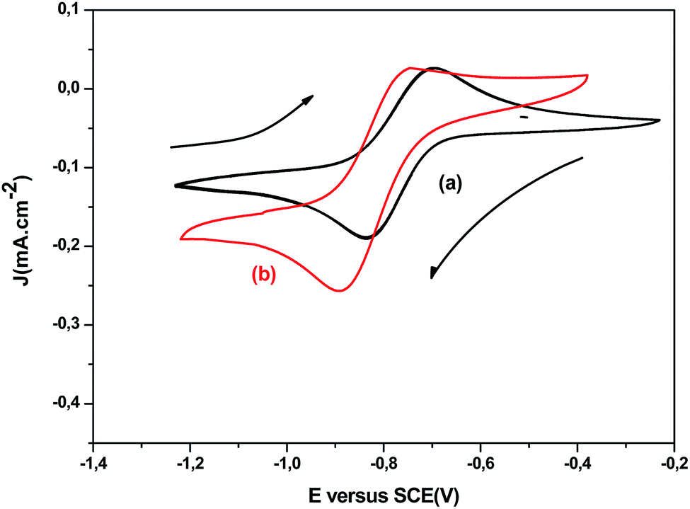
CV was employed to optimize deposition potential on the ITO working electrode of Cu2+, In3+, and Ce3+ electroactive species. It is well known, the standard reduction potential of Cu, In, and Ce are 0.14 V, −0.58 V and 1.22 V (vs. SCE), respectively.20 Thus, the cathodic reactions on ITO electrode of both systems (Cu–In) and (Cu–In–Ce) cannot be expected owing to large standard potential difference. Both systems were adjusted to pH = 2.0 with 10−3 mol L−1 TEA solution as chelating agents to reduce the wide reduction potential. Firstly, CV curves with TEA (not shown) were employed to achieve the thermodynamic features of each species independently in plating solution bath. Subsequently, the CV of both binary (6 mg InCl3, 12 mg CuCl2) and ternary (6 mg InCl3, 12 mg CuCl2+ 0.2–0.6 mg CeCl3) systems were recorded at a fixed scan rate of 20 mV s−1 at room temperature 300 K. It is worth noting that the cyclic voltammograms presented a prominent cathodic peak around −0.85 V in the forward scan matched to the reduction of both species Cu2+ and In3+ on ITO electrode, which is ascribed to the formation of CuIn alloys as displayed in Fig. 1a. These results are previously reported by Cummings et al.21 However, a slight shift towards negative potential was detected for reduction peak upon the addition of CeCl3 to Cu–In binary system at almost the same intensity as shown in Fig. 1b. It can be inferred that to the incorporation of Ce into the Cu–In phase, so, the establishment of CICe ternary alloy at this range of potential lies between −0.80 V and −1.0 V. Moreover, a weak and wide oxidation peak detected at −0.80 V involves partial dissolution of the solid solution of Cu–In–Ce system, which means that the electrodeposition process is irreversible. The finding shows that the voltammetry studies does not look a classic metal electrodeposition process, which denotes that the reduction of cerium species is associated probably to surface phenomena and not to the depletion of cerium ion at the reaction interface.
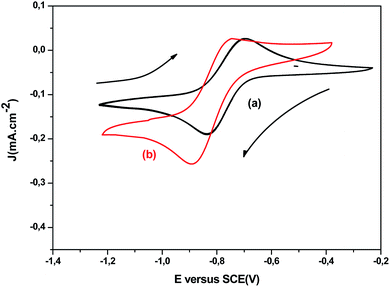 |
| | Fig. 1 Cyclic voltammograms of 6 mg InCl3, 12 mg CuCl2 (a) and 0.6 mg CeCl3, 6 mg InCl3, 12 mg CuCl2 (b) recorded on ITO working electrode immersed in aqueous acidic plating bath (pH = 2) at room temperature using scan rate 20 mV s−1. | |
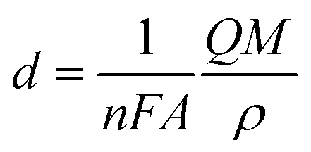
In order to achieve a dense and homogeneous film without holes and cracks, we kept the potential bias at −0.9 V with an optimized deposition time of 3 min. Therefore, we can estimate the thickness of CICe alloys by using the following equation:
| |
 | (1) |
where
n = 8 is the number of electrons,
F = 96
![[thin space (1/6-em)]](https://www.rsc.org/images/entities/char_2009.gif)
485 C mol
−1 is Faraday constant,
Q is the oxidation charge,
A is the electrode area,
M = 318
486 g mol
−1 is the molecular weight, and
ρ ≈ 7.32 g cm
−3 is the density of CICe alloys. The obtained thickness is about 1.5 μm, which is in good agreement with profilometer measurements.
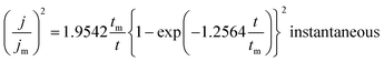
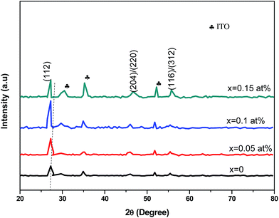
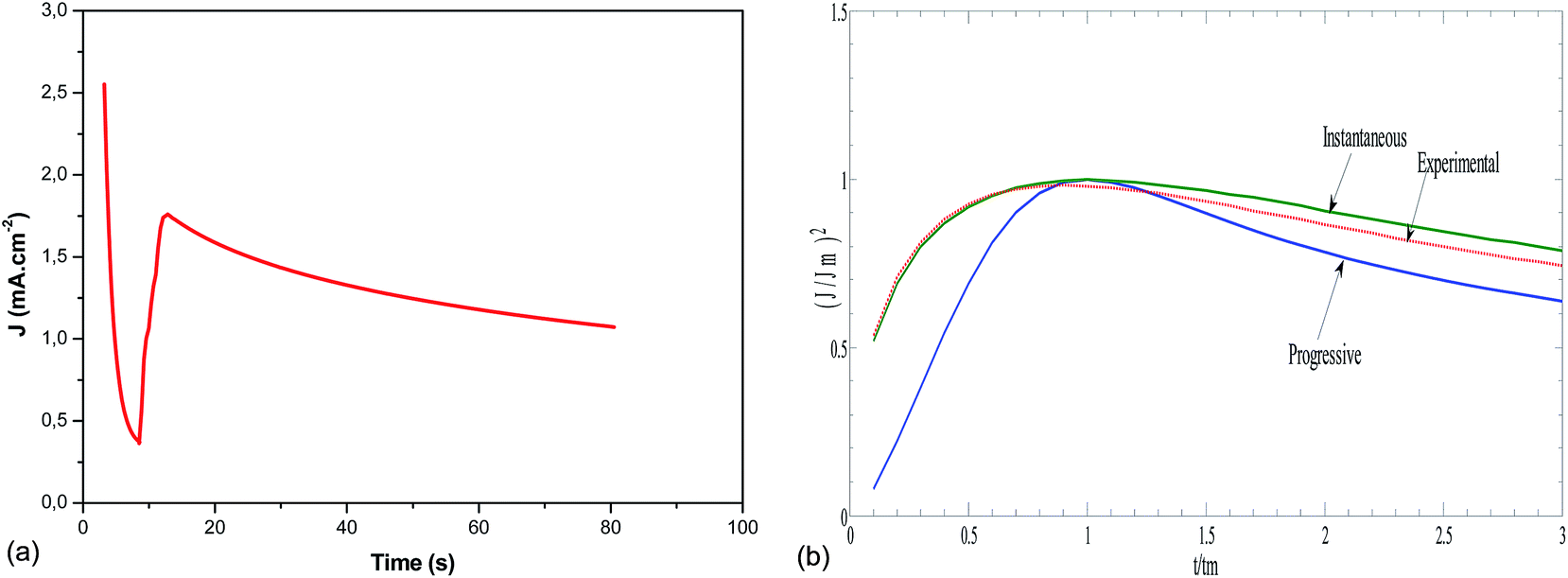
On the other hand, the nucleation kinetics and the growth pathways of the first nuclei created on the ITO substrate are crucial steps that monitor the morphology and microstructure properties of the electrodeposited CICe alloys. Thus, CA was employed to probe further the nucleation and growth mechanism responsible for the electrodeposition of CICe alloys. The current density is recorded at a constant potential −900 mV over time scale for 80 s, at which the electrodeposition of CICe alloys is achieved from the open-circuit potential. As can be seen from Fig. 2a, the typical shape of the curve approves the initial stage of the electrocrystallisation of CICe alloys on ITO substrate. The first step of CICe alloy nucleation process, the current density drops abruptly owing to double-layer charge between the ITO surface and the electrolyte with the close stirred growth of CICe alloy. Subsequently, the current density increases promptly to a maximum value jmax reached at tmax owing to the linear diffusion of the electroactive ions towards the ITO electrode. Indeed, during this step the nuclei develop diffusion zones around themselves, as the zones overlap the hemispherical mass transfer. This kinetics was also previously reported by Xu et al.22 Beyond the last step, the current density decays gradually over the time, which suggests the incessant synthesis of CICe alloys due to rise of the electroactive surface area. Among various models suggested to illustrate the CA curves for instantaneous and/or progressive nucleation of three-dimensional (3D) hemispherical nuclei with growth rates controlled by ion volume diffusion (Vd) is the outstanding Scharifker–Hills theoretical model. The governing equations for the two nucleation mechanisms are given below:
| |
 | (2) |
| |
 | (3) |
where
J is the current density at time
t, and
Jm is the maximum current density at time
tmax.
Fig. 2b depicts quite good agreement between the experimental and theoretical instantaneous nucleation curves ensuring the three-dimensional growths of Cu–In–Ce alloys on the ITO working electrode. Afterwards, all the obtained samples were carried out to sulphurisation process as mentioned in the experimental section.
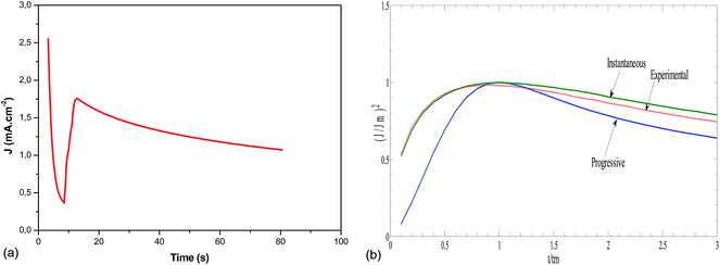 |
| | Fig. 2 (a) The current–time transient resulting from chronoamperometry experiment for the deposition of CICe alloys in company of (6 mg InCl3, 12 mg CuCl2 + 0.6 mg CeCl3) and 10−3 mol L−1 TEA at a fixed potential −0.9 V vs. SCE. (b) The nondimensional plots of (J/Jm)2 versus t/tm for elucidating the nucleation growth mechanism of Cu–In–Ce alloy electrodeposited from a plating solution bath containing (6 mg InCl3, 12 mg CuCl2 + 0.6 mg CeCl3) and 10−3 mol L−1 TEA. | |
3.2 Structural characterization
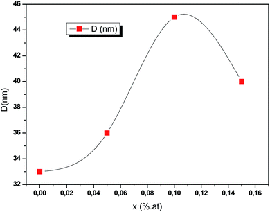
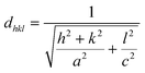
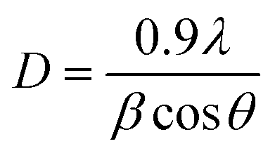
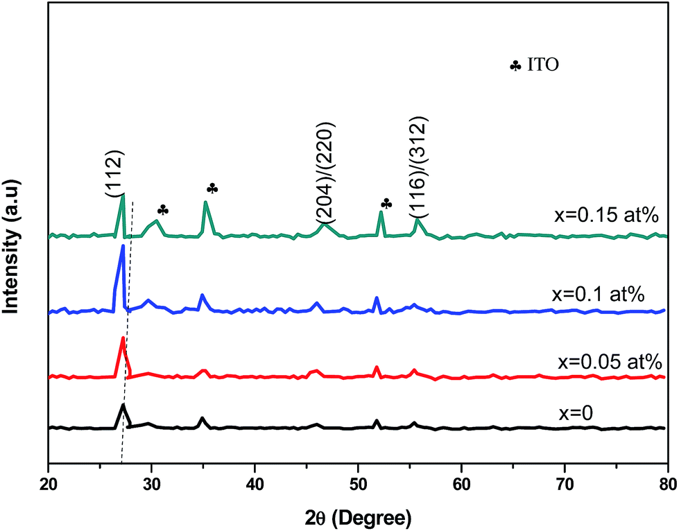
The room-temperature crystalline structure of undoped and Ce-doped CIS thin films deposited on ITO substrates and annealed at 300 °C are shown in Fig. 3. All the samples display a multiple diffraction peak corresponds to (112), (204)/(220), and (116)/(312) planes located near 27.81°,46.43° and 55.01°, respectively. This result confirms the polycrystalline nature of synthesized CICS films. All the diffraction peaks were indexed by matching with the standard data from JCPDS (Joint Committee on Powder Diffraction Standards) database for CIS and ITO with card numbers (47-1372) and (06-0416), respectively. It is established that the deposited CICS films belong to chalcopyrite phase with tetragonal structure and I![[4 with combining macron]](https://www.rsc.org/images/entities/char_0034_0304.gif) 2d space group. It is observed a stronger intensity peak obtained for CIS thin film around 2θ = 27.81° matches to the preferential orientation along (112) plane. Moreover, no trace of other secondary phases, indicating that the Ce3+ ions prefer to substitute In3+ ones in the CIS lattice rather than existing as another phase. It is also worth noting that the intensity peaks of (112) plane increase as Ce contents increases. Nevertheless, for x > 0.1 the intensity of diffraction peaks drops, which attributes that the Ce3+ ions were heavily incorporated into the host matrix and so randomly fluctuating the nucleation and growth processes of the deposited CICS thin films. In addition, the preferential diffraction peaks for CICS film shift somewhat to smaller 2θ value, which demonstrates that Ce3+ ions have been successfully incorporated into the host matrix as shown in Fig. 3. Similar results have been reported in some aforementioned survey.16,23 According to the preferential diffraction peaks of (112) plane, the average crystallites size was estimated using Debye–Scherrer equation:24
2d space group. It is observed a stronger intensity peak obtained for CIS thin film around 2θ = 27.81° matches to the preferential orientation along (112) plane. Moreover, no trace of other secondary phases, indicating that the Ce3+ ions prefer to substitute In3+ ones in the CIS lattice rather than existing as another phase. It is also worth noting that the intensity peaks of (112) plane increase as Ce contents increases. Nevertheless, for x > 0.1 the intensity of diffraction peaks drops, which attributes that the Ce3+ ions were heavily incorporated into the host matrix and so randomly fluctuating the nucleation and growth processes of the deposited CICS thin films. In addition, the preferential diffraction peaks for CICS film shift somewhat to smaller 2θ value, which demonstrates that Ce3+ ions have been successfully incorporated into the host matrix as shown in Fig. 3. Similar results have been reported in some aforementioned survey.16,23 According to the preferential diffraction peaks of (112) plane, the average crystallites size was estimated using Debye–Scherrer equation:24| |
 | (4) |
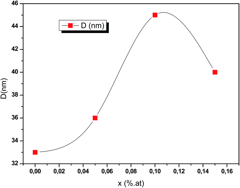
where λ is the incident X-ray wavelength, β is the peak of the width at the half-maximum (FWHM) intensity (rad) and θ is the diffraction angle (degree). Fig. 4 exhibits that for greater doping contents (0.15 at%) the average crystallite size is raised when compared to that of pure CIS and is dropped when compared to that of CIS doped with 0.1 at%. It is found that the average crystallites size lies between 33 nm and 45 nm with respect to systematic rise in the Ce content up to 0.1 at%.
 |
| | Fig. 3 X-ray diffraction patterns of annealed CICS thin films deposited on ITO-coated glass substrates at room temperature with various cerium contents. | |
 |
| | Fig. 4 Crystallites sizes of obtained CICS films on ITO-coated glass substrates as a function of cerium contents according to the prominent diffraction peaks of (112) plane. | |
The estimation of average crystallites size of CICS films is a little higher compared with those obtained by J. Zhu et al.16 as the cerium content increases. This might be due to the process used in the synthesis of CICS films.
For all CICS films, the lattice parameters a and c were estimated via the Cohen method,25 where the inter-planar distances for tetragonal structure (a = b ≠ c) are given by the following relation
| |
 | (5) |
As plotted in Fig. 5, we see that the lattice parameters (a = b ≠ c) of the CuIn1−xCexS2 (x = 0, 0.05, 0.1, 0.15) films are larger than that of the CIS film since the ionic radius of Ce3+ (r = 0.101 nm) is much greater than that of In3+ (r = 0.081 nm) one.26,27 Consequently, the (112) diffraction peaks of doped samples underwent a slight shift toward a lower angle as shown in Fig. 3. The lattice parameters determined in the present work are close to results reported previously by Xiao et al.23
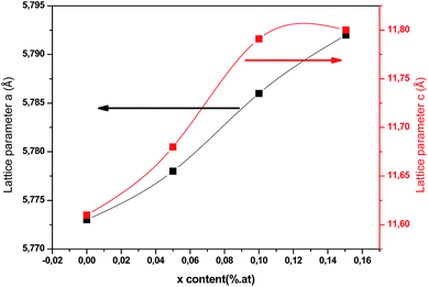 |
| | Fig. 5 Lattice parameters (a and c) of annealed CICS films deposited at −0.9 V versus SCE for 3 min on ITO-coated glass substrates versus cerium contents. | |
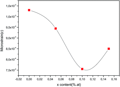
On the other hand, the microstrain (ε) values of undoped and Ce doped CIS films were calculated using the relation:28
| |
 | (6) |
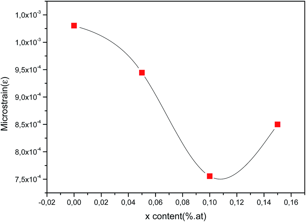
As can be seen from Fig. 6, the estimated microstrain values dropped with rising cerium content until 0.1 at% and then decreased. As known, the lower value of microstrain owing to a greater degree of crystallinity and to lower structural defects. So, it can be inferred that because of lattice expansion of the unit cell, microstrain is reduced and it results in the boost of crystallites size of the films with increasing Ce content.
 |
| | Fig. 6 Microstrain (ε) of obtained CICS films deposited at −0.9 V versus SCE on ITO glass substrate as function of cerium contents. | |
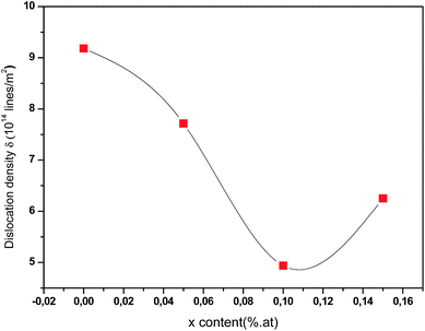
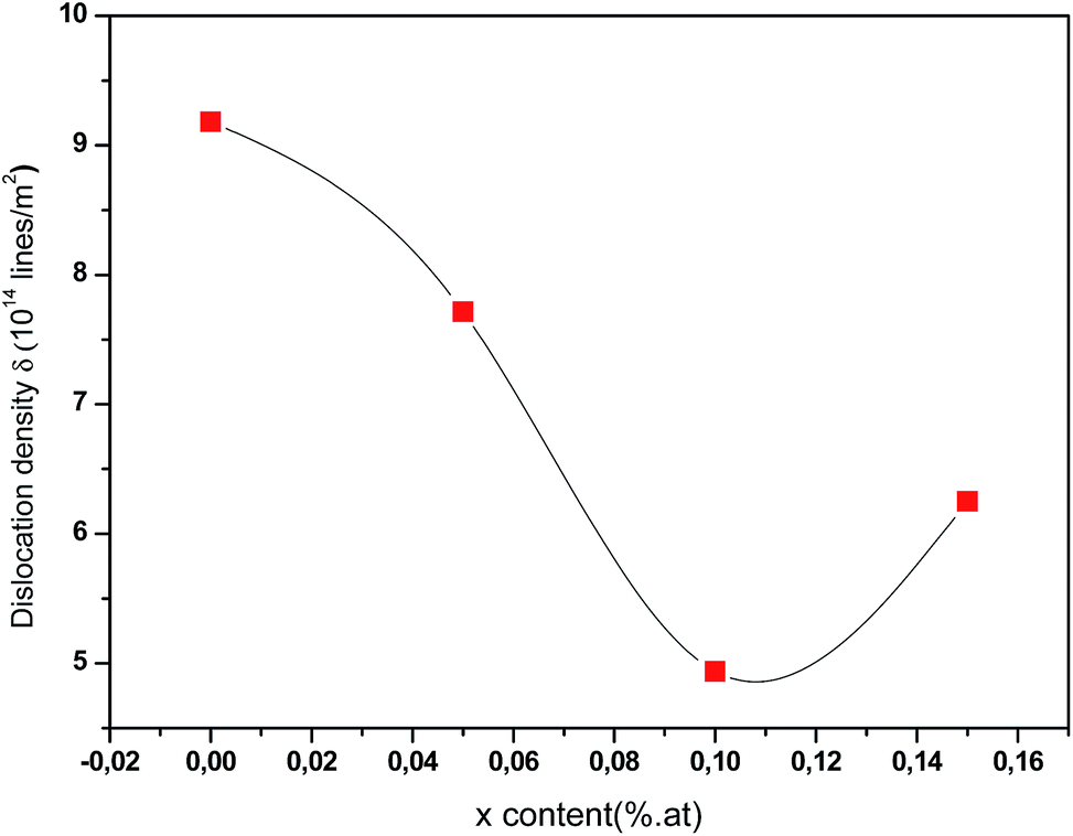
Dislocation density (δ) defined as the length of dislocation lines per unit volume of the crystal is expressed with the help of Williamson and Smallman's equation29
| |
 | (7) |
Fig. 7 displays the variation of dislocation density versus Ce contents. As can be seen, the dislocation density values initially decrease then increase with increasing Ce contents. The increase in dislocation density suggests that there is a reduction of crystallites size so, films become less crystalline. However, the small value of ‘δ’ obtained for 0.1 at% of Ce in the current study approves that electrodeposition is an effective technique to deposit good quality polycrystalline CICS thin films. From the reflections of XRD patterns, it is established that 0.1 at% of Ce3+ doped CIS thin films have good crystallinity, low strain, and less dislocation density when compared with the other samples.
 |
| | Fig. 7 Dislocation density (δ) of annealed CICS films deposited at −0.9 V versus SCE for 3 min on ITO-coated glass substrates as a function of cerium contents. | |
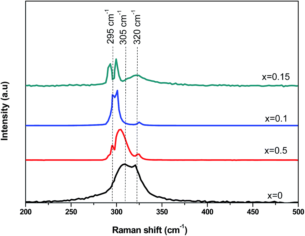
In order to further investigate the microstructures of the CICS thin films, Raman spectroscopy is used to obtain more information related to the active vibrations modes of synthesized films and to provide insights on the doping effects. According to group theory, CIS material exhibits two completely symmetric (A1) modes, namely, chalcopyrite (CH) phase and Cu–Au (CA) ordered phase, which acts at 295 cm−1 and 305 cm−1, respectively.30,31 Fig. 8 depicts the Raman spectra of the CICS thin films deposited at different Ce contents by helium neon laser (632.81 nm) at the frequency range lies between 200 and 500 cm−1 at room temperature. As can be seen, all the samples indicate the presence of broad peaks matches to typical modes of CICS lattice vibration of the chalcopyrite structure namely (CH) and (CA) phases probed near 295 cm−1 and 305 cm−1, respectively. Additional wide peaks near 320 cm−1 are detected for all CICS films assigned to β-In2S3 as secondary phase.32 It seems to be mismatched with XRD results while their Raman spectra display the existence of this phase. This discrepancy could be explained by the fact that the wavelengths used by XRD and Raman apparatus have altered penetration depths in the CICS thin film. It is should be noted that both the CH and CA ordered phases intensity increases and its FWHM decrease with increasing Ce content up to 0.1 at%. Moreover, as Ce contents increase the position of prominent peaks corresponds to CH ordered phase somewhat shift to lower wave number about ∼5 cm−1, which is attributed to a partial substitution of In ions by Ce ones since the molecular weight of Ce element is about 23% more than In one. It is also interesting to notice that the Cu2−xS phase impurities are not recorded in 470 cm−1 owing to etched samples in KCN solution to remove any sulfur-related compounds subsequent to the deposition of CICS films, which is in excellent agreement with the XRD results.
 |
| | Fig. 8 Raman spectra of annealed CICS films deposited at −0.9 V versus SCE for 3 min on ITO-coated glass substrates as a function of cerium contents. | |
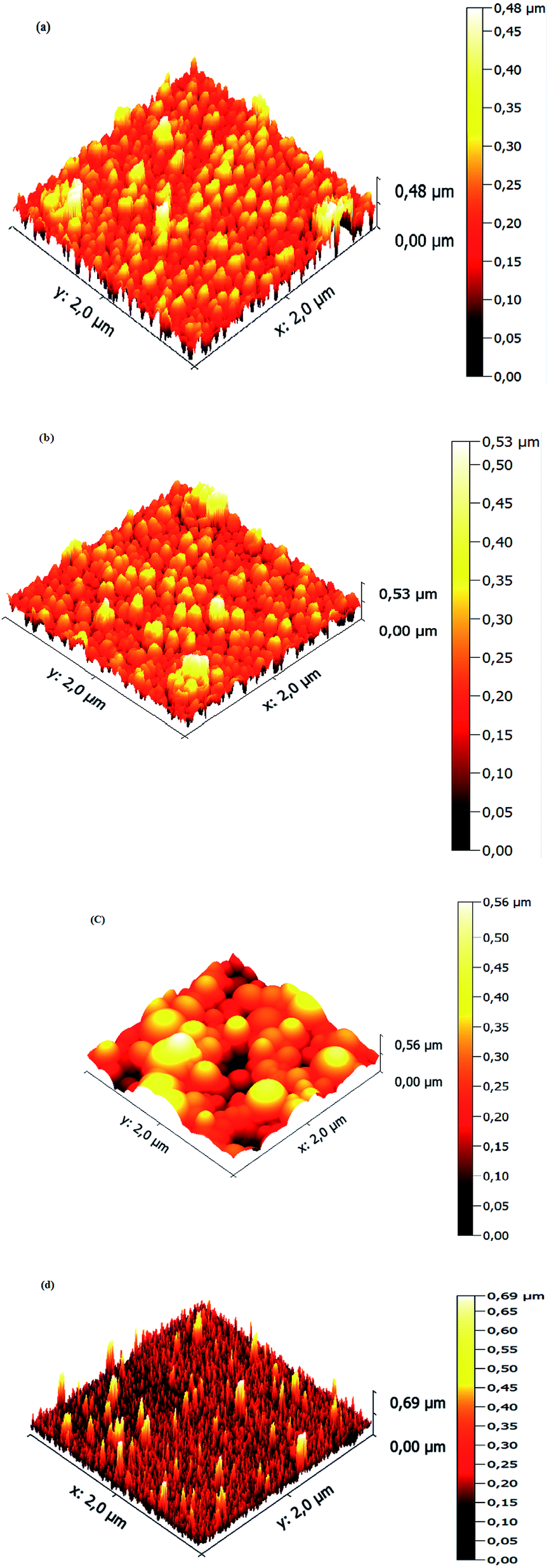
3.3 Morphological analysis
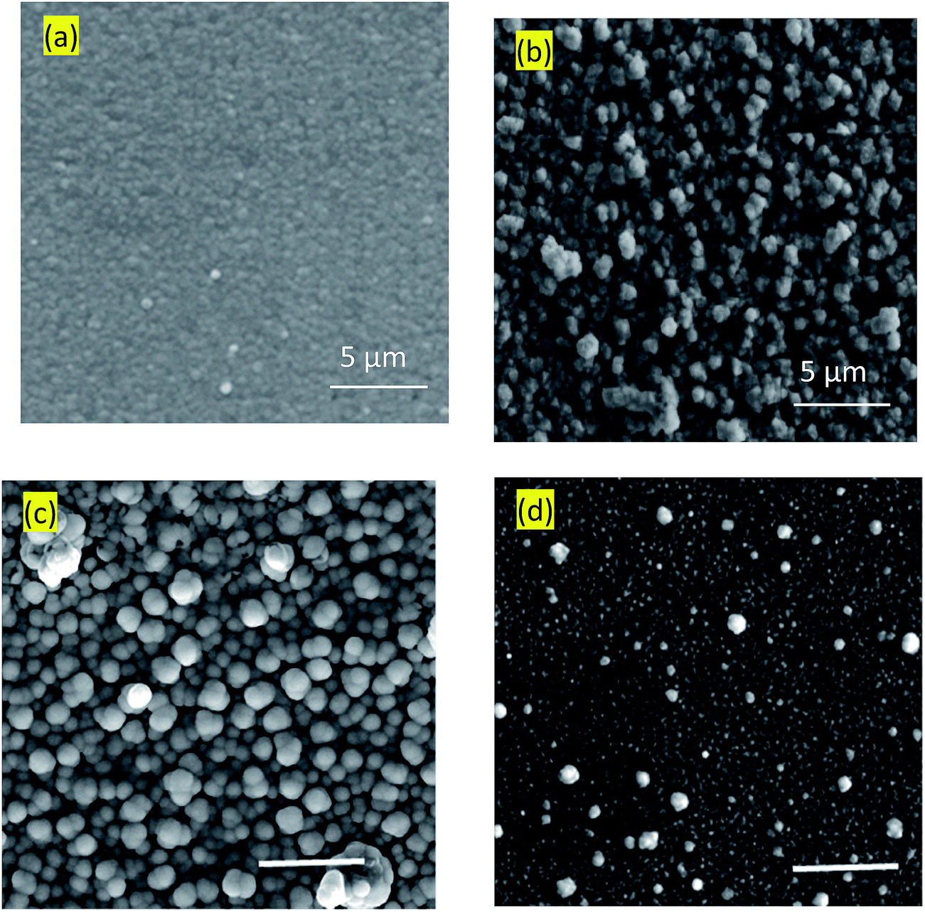
Surface microstructures and roughness of CICS thin films play a critical role in the development of photovoltaic devices and/or photoelectrochemical hydrogen production. In this work, SEM and AFM images scanned over a surface area of 2 × 2 μm2 were employed to monitor surface morphology and roughness of CICS thin films. The surface microstructures of obtained CICS thin films grown on ITO glass substrates are exhibited in Fig. 9(a)–(d), respectively. As can be seen, the surface morphology and grain size of the CICS samples were affected by various Ce3+ doping contents. According to Fig. 9(a), the surface morphology of undoped CIS thin films shows minor grains size homogeneously distributed with spherical shapes. As the level of Ce-doping is increased to 0.1 at%, the surface flower-like microstructure becomes more uniform and improvement of grain sizes, which might be attributed to fewer grains boundaries so to enhancement in crystal quality. However beyond 0.1 at% of Ce content, the surface microstructure of the film shows an uneven grains size with an additional few spherical agglomerates, disjointed from the rest of the structure as shown in Fig. 9(d). This follows from the fact that randomly distributed nuclei designed primary growth into noticeable grains since the crystallization progression include several phases of nucleation and coalescence throughout the incorporation of Ce3+ inside the host matrix. In addition, the grain sizes of the CICS films gradually increased from 10 nm to 100 nm when Ce3+ contents increase up to 0.1 at% and drops after that. This was probably due to the increased surface migration energy of the adatoms with the increase in Ce3+ doping contents. As far as AFM is concerned, the 3D images recorded to examine the surface roughness of the CICS films are shown in Fig. 10(a)–(d). The measured root mean square (RMS) with AFM for the four samples was estimated by the following equation:33| |
 | (8) |
where N is the number of height measurements, Zj the vertical coordinate of the image, and ![[Z with combining macron]](https://www.rsc.org/images/entities/i_char_005a_0304.gif) the mean value of the Zj. The calculated values are exhibited in Table 1. As can be seen from Table 1, compared with the un-doped CICS films the RMS values for the Ce-doped samples have been remarkably altered by the Ce-doping. In particular, the RMS value for the Ce-doped sample 0.1 at% is even larger than the other samples. The roughest surface morphology achieved for the Ce-doped sample 0.1 at% could be ascribed to the rise in grain size of the films. The latter behavior is in good agreement with the XRD analysis. Hence, the optimal doping content for the preparation of CICS films can be confirmed to 0.1 at%.
the mean value of the Zj. The calculated values are exhibited in Table 1. As can be seen from Table 1, compared with the un-doped CICS films the RMS values for the Ce-doped samples have been remarkably altered by the Ce-doping. In particular, the RMS value for the Ce-doped sample 0.1 at% is even larger than the other samples. The roughest surface morphology achieved for the Ce-doped sample 0.1 at% could be ascribed to the rise in grain size of the films. The latter behavior is in good agreement with the XRD analysis. Hence, the optimal doping content for the preparation of CICS films can be confirmed to 0.1 at%.
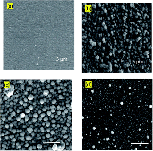 |
| | Fig. 9 Typical SEM images of annealed CICS thin films deposited on the ITO-coated glass substrates with various cerium contents (a) undoped (b) 0.05 at% (c) 0.1 at% (d) 0.15 at%. The scale bar denotes 5 μm. | |
 |
| | Fig. 10 3D AFM images of annealed CICS thin films deposited on the ITO-coated glass substrates with various cerium contents (a) undoped (b) 0.05 at% (c) 0.1 at% (d) 0.15 at%. | |
Table 1 Roughness and EDS quantitative results of obtained CICS thin films
| Samples |
Roughness (nm) |
Percentage of element (at%) |
| Cu |
In |
Ce |
S |
| 1 |
5.73 |
26.56 |
15.83 |
0 |
57.45 |
| 2 |
9.41 |
27.43 |
15.64 |
1.31 |
56.65 |
| 3 |
10.34 |
27.57 |
14.96 |
2.56 |
57.01 |
| 4 |
8.66 |
27.19 |
14.43 |
3.27 |
57.11 |
According to chemical compositional achieved by means the EDS. The doping process was successfully achieved within the synthesized thin films and the atomic percentage of each element is presented in Table 1. As expected, an increase in the Ce content along with a decrease in In content is observed.
3.4 Optical proprieties
The experimental measurement of transmission T(λ) and reflection R(λ) is carried out by using an UV-vis-NIR spectrophotometer in the range of wavelengths between 300–1500 nm to compare the effect of Ce doping on the optical energy band gap of CICS film. The optical band gap of CICS thin films deposited on ITO substrates at 350 °C was estimated from transmittance and reflectance spectra in the incident photon energy (hν) lie between 0.8 eV and 2 eV. The absorption coefficient of CICS thin films is determined from the following equation:| |
 | (9) |
where α is the absorption coefficient, T is the transmittance, R is the reflectance, and d is the thickness of CICS thin films in cm.
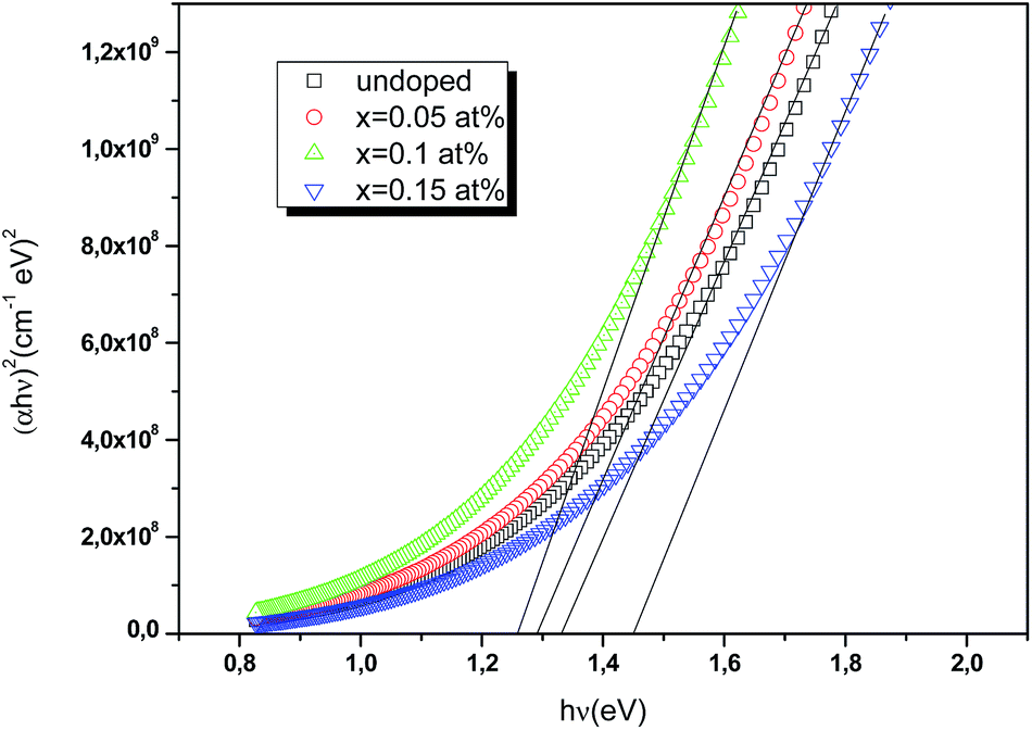
The energy of the optical bandgap (Eg) is determined using Tauc relationship34 between the absorption coefficients (α) in the high absorption region (α > 104 cm−1) and the incident photon energy (hν) confirming to the following equation:
where
h is the Planck constant,
ν is the frequency of the incident photon,
A is a constant, and
n is a constant representing the type of electronic transition. It is well known that
n is equal 2 for an indirect band gap and 1/2 for a direct band gap.
35 From the theoretical and experimental results, CIS film is well known to be a direct band gap material.
36,37 To estimate the direct optical band gap of CICS films, we plot the variation of (
αhν)
2 versus hν and fitting the straight line part to
hν axis
i.e. (
αhν)
2 = 0. Hence, the point of intersection of the linear fit to the
x-axis provides the energy of the optical band gap. The values of direct optical bandgaps are gradually decreased from 1.32 to 1.26 eV as Ce doping increases from 0 to 0.1 at%. Beyond this Ce doping value 0.1 at%, the energy band gap increases to 1.43 eV as shown in
Fig. 11. The tuning of the band gap can be explained as follows: when crystallite sizes increases, microstrain decreases, which leads to the formation of high-quality films with enhancements in the crystallinity structure and thus to red shift the optical bandgap. A similar result has been observed by Cui
et al.38 concerning the variation in optical bandgaps when Ag doped SnS
2 photocatalyst. However, the observed blue shift of the optical band gap is attributed maybe to lattice expansion in CICS films since Ce ions are larger than In ones, in addition to shrinking of the quantum size effect.
39 The measured values in this study are lower than reported Xiao
et al.23 The difference is probably ascribed to the technical synthesis of CICS films. The chemical composition dependence of the optical energy band gaps in the electrodeposited of CICS films is supposed to originate from the combined effects of both a cerium doping and a solid solution formation. A similar tendency was found in the case of Ga-doped ZnO by Thambidurai
et al.40 The results of this investigation demonstrate that optical band gap is altered by cerium contents. In particular, when
x = 0.1 the optical band gap of the CuIn
0.9Ce
0.1S
2 compound is about 1.26 eV which considered an appropriate absorber layer for thin film solar cells.
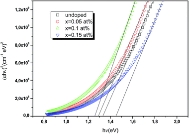 |
| | Fig. 11 Plots of (αhν)2 versus incident photon energy (hν) to estimate the optical band gap of undoped and Ce doped CIS thin films. | |
3.5 Electrical proprieties
M–S measurements provide essential information about the semiconducting properties of CICS in contact with electrolytes. To investigate the effect of Ce dopants on the electrochemical properties, the M–S plots of CICS films were recorded in 0.5 M K2SO4 aqueous solution (pH = 7) since ionic liquids can provide a large potential window without altering CICS film. It is generally expected that the capacitance at the semiconductor–electrolyte interface is controlled by that of the semiconductor. Thus, to evaluate the conduction type, the flat band potential (Vfb) and carrier densities (N) of CICS films, we apply Boltzmann statistics to obtain Mott–Schottky equation given as follows:41| |
 | (11) |
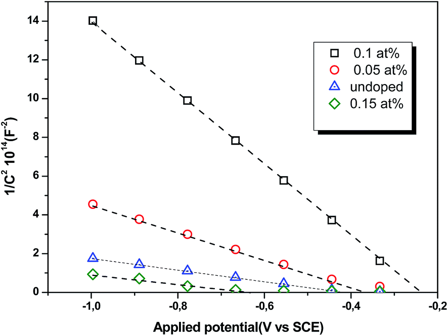
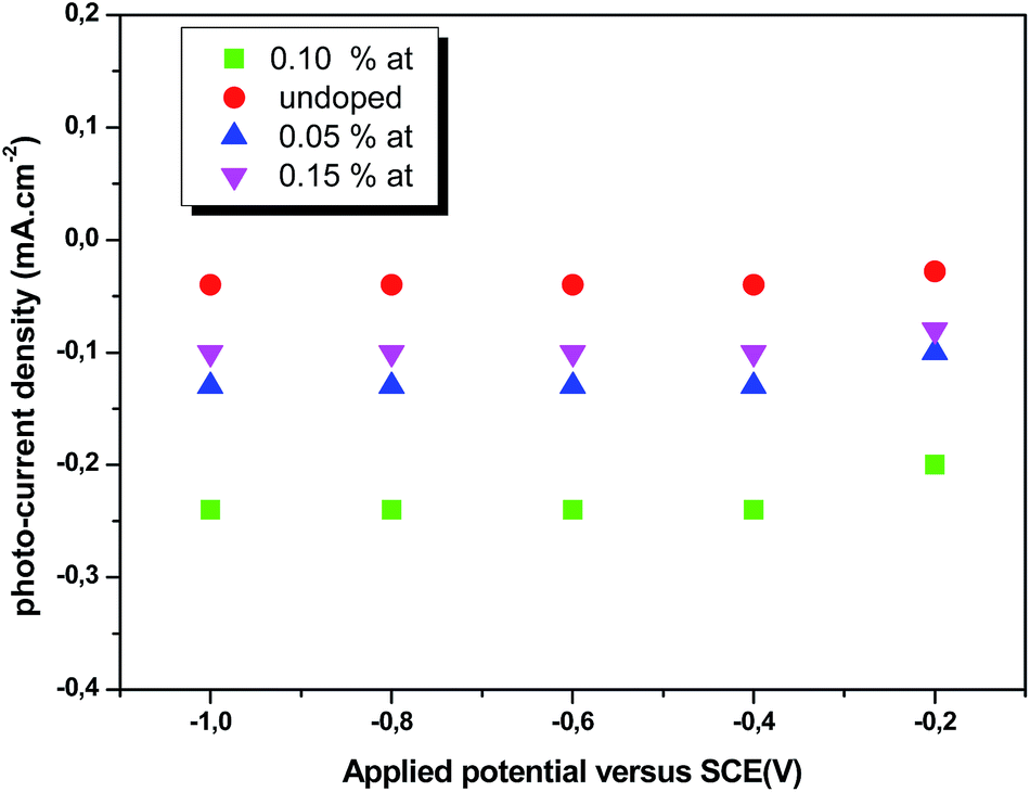
where Csc denotes the space charge capacitance of the depletion region in F cm−2, q the electron charge in C, ε0 the vacuum permittivity (8.8 × 10⁻¹⁴ F cm−1), εr = 10 the semiconductor dielectric constant,42,43 V the applied bias voltage, kB the Boltzmann constant (1.38 × 10⁻²³ m2 kg s−2 K−1), T the absolute temperature in K, N the majority charge density of donors or acceptors in the semiconductor (cm−3), and A is the electrode surface area in contact with the electrolyte (∼1 cm2). Vfb is the flat band potential of the semiconductor, which reflects the Fermi level of semiconductor (V). The term  is usually insignificant and can be neglected at room temperature. As can be observed in Fig. 12, all the M–S curves of CICS films exhibited negative slopes, indicating all the samples revealed p-type electrical conductivity, which is consistent with other previous reports.44 According to eqn (9), the carrier density in photo cathodes is inversely proportional to the slopes of linear parts of M–S plots and the flat-band potentials of each sample can be obtained from the intercept on the x-axis in the linear region of the curves. It is found that the hole acceptor density calculated from slopes of M–S plots of the CICS samples decreases with the Ce contents from 4.8 × 1016 cm3 (undoped films) to 7.6 × 1015 cm3 at (0.1 at% Ce doped films) and then increases to 5.7 × 1016 cm3 when cerium contents reach 0.15 at% in the dark condition. This may be attributed to minor phase segregation of Ce in CICS films. The phase segregation of Ce in CICS film reveals the effect of decrease in Cu vacancies VCu, which becomes smaller in CICS films with further increase Ce contents. Thus, the Ce contents acts as an electrical dopant to decrease the hole acceptor density, which is consistent with previous reports.45 Nevertheless, it seems that our outcomes were disagreeing to some previous reports claiming that Zn, Sb and Ni ions one could improve the charge carriers of CIS films.46 On the other hand, the flat-band potentials were extrapolated to −0.41–0.35 V and −0.25 V vs. SCE with the rise of Ce content up to 0.1 at% and noticeably decreases to −0.63 V thereafter, which means that flat band potential is shifted towards more cathodic potentials beyond 0.1 at% of Ce content. This result is consistent with the change trend of charge carriers density since the smaller value of carriers' density for the Ce doped CIS samples reveal a smaller flat band potential than that of undoped CIS film. These results of flat band potentials of CIS thin films are slightly higher than those reported by Tang et al.47 To examine the potential of the synthesized CICS films for solar energy harvesting, the photo electrochemical features were settled by analyzing the photocurrent density response using the chopping method for assessing the current in dark and light conditions.48 Fig. 13 compares the photocurrent-generation behavior of undoped and Ce doped CIS films at external applied bias voltages lies between −1.0 to −0.4 V vs. SCE in the dark and under illumination conditions. It is should be noted, no degradation of the films was perceived during photo electrochemical measurements. In addition, the photocurrent density is on the negative potential area proves that all the samples are p-type conductivity, which is in well agreement with Mott–Schottky plots. On the other hand, the photocurrent density is insignificant of all the CICS samples over applied potentials range between −1.0 to −0.4 V vs. SCE in the dark condition. While, under illumination the CICS films exhibits an increase in photocurrent density with increasing the cathodic potential. The maximum photocurrent density was reached 24 mA cm−2 with an external bias potential −0.4 V vs. SCE and sample with 0.1 at% Ce content. Additionally, as the cathodic potential increases further, the photocurrent density is approximately constant. It is inferred that the optimal potential should be taken −0.4 V to examine the electrochemical photocurrent responses of CICS thin films.
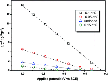 |
| | Fig. 12 Mott–Schottky plots of CICS thin films recorded in 0.5 M K2SO4 aqueous solution (pH = 7) versus the range of applied potential at room temperature. | |
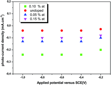 |
| | Fig. 13 Photocurrent generated using CICS/ITO electrode at different applied potentials vs. SCE for samples in 0.5 M K2SO4 electrolyte (pH = 7) at room temperature. | |
Fig. 14(a)–(d) displays the effect of Ce contents on photocurrent–time transient responses of CICS thin films measured at optimal applied bias potential −0.4 V vs. SCE during 400 s. It can be noticed, in the dark, all the CICS films exhibited small currents with slight difference. In addition, all the samples exhibited enhanced cathodic current density under light illumination, which is characteristic of a semiconductor with p-type conductivity. These findings agree well with results obtained from M–S plots. It should be noted that the stability of the photocurrent density for all the samples during the test. The variation of photocurrent density was established for numerous sequences of illumination. It is well known, the photo enhancement current density is the variance between photo-current density and dark-current density. The photo-current density responses increase from 4 mA cm−2 to 24 mA cm−2 with the addition of Ce contents up to 0.1 at% and then decrease until 10 mA cm−2. The dependence of the photocurrent density response on the Ce contents is probably ascribed both to grain size and the band gap of CICS thin films. Indeed, when the Ce content exceeds 0.1 at%, the grain size and the band gap of CICS samples decreased foremost to higher recombination of photo-excited electrons–hole pairs. Thus, the photocurrent density response decreased. In spite of the highest carriers' density, the surface states of samples with Ce content 0.15 at% can contribute significantly to decrease of photocurrent density response owing to uneven grain growth and microstructure as mentioned previously in Section 3.3. Consequently, carriers' densities are not the main factor elucidating the decrease in the photocurrent density. In a comparison of the photocurrent densities produced by CICS with Ga doped CIS thin film fabricated using the same electrodeposition technique. The photocurrent density in the current study is three times higher than CIGS photocathodes formed by Mandati et al.49 Nonetheless, this was of the same magnitude as previously reported by Chae et al.50 The improved photo response of deposited CICS films with 0.1 at% indicates their eventually potential application for photoelectrochemical hydrogen evolution reaction.
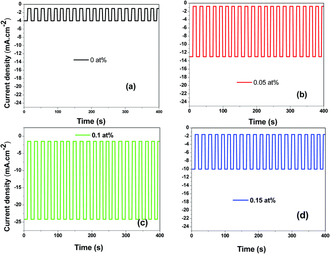 |
| | Fig. 14 Photocurrent responses of the obtained CICS films grown on ITO substrate under light-emitting diode (LED) in the visible range. | |
4. Conclusion
In this study, CuIn1−xCexS2 (CICS) thin film was synthesized on a transparent ITO substrate via green and low-cost electrochemical method for either photovoltaic device or photoelectrochemical water reduction. The effect of cerium content in solution bath on the structural, morphological, optical and photoelectrochemical properties of CICS thin films was investigated. Electrochemical measurement exhibited two notable results: on the one hand, a prominent cathodic peak lies between −0.85 V and −1 V matches to the formation of CICe alloys on ITO substrate during the forward scan towards the negative potentials. On the other hand, analysis of the chronoamperometry data obtained at fixed potential −0.9 V revealed that nucleus growth mechanism during the process is denoted by the instantaneous nucleation model. XRD analysis of annealed CICS thin film crystallizes well in a tetragonal chalcopyrite structure with (112) preferential crystallographic orientation. According to spectrophotometric data, the estimated direct optical band gap of CICS thin films can be tuned from 1.26 eV to 1.43 eV by means of cerium dopant concentration, which is more favorable for solar cell applications compared to CIS films. On the other hand, the carrier densities and flat-band potentials of the CICS films achieved from Mott–Schottky were found to lie between 7.6 × 1015 cm3 to 5.7 × 1016 cm3 and −0.25 to −0.63 V vs. SCE, respectively. All the CICS films present p-type semiconductor using both the M–S plot and photocurrent–time transient response measurements. Since the photo-current density response reaches 24 mA cm−2 for CICS film with Ce content 0.1 at%, we can expect an enhancement of CIS photo absorber for PEC applications. It is our belief that this research can further enhance the development of rare earth elements (R) doped CIS films as a photocathode material for future CIRS solar cell applications and photoelectrochemical hydrogen evolution.
Acknowledgements
This work was financially supported by the Center of Research and Technology of Energy, Technopole of Borj Cedria, Tunisia.
References
- T. Nakada, Electron. Mater. Lett., 2012, 8, 179 CrossRef CAS.
- M. A. Green, K. Emery, Y. Hishikawa, W. Warta and E. D. Dunlop, Prog. Photovoltaics, 2013, 21, 827 Search PubMed.
- Y. Huang, A. Han, X. Wang, X. Liu, Z. Liu and F. Meng, Mater. Lett., 2016, 182, 114–117 CrossRef CAS.
- S. J. Heise, V. Gerliz, M. S. Hammer, J. Ohland, J. Keller and I. Hammer-Riedel, Sol. Energy Mater. Sol. Cells, 2017, 163, 270–276 CrossRef CAS.
- Q. Li, L. Zhai, C. Zou, X. Huang, L. Zhang, Y. Yang, X. Chen and X. Huang, Nanoscale, 2013, 5, 1638–1648 RSC.
- P. Jackson, R. Wuerz, D. Hariskos, E. Lotter, W. Witte and M. Powalla, Phys. Status Solidi RRL, 2016, 10, 583 CrossRef CAS.
- Z. Yan, W. Deng, X. Zhang, Q. Yuan, P. Deng, J. Liang and L. Sun, Phys. Status Solidi A, 2014, 211(11), 2546–2551 CrossRef CAS.
- P. M. P. Salomé, H. Rodriguez-Alvarez and S. Sadewasser, Sol. Energy Mater. Sol. Cells, 2015, 143, 9–20 CrossRef.
- T. Connor, B. D. Weil, S. Misra, Y. Cui and M. F. Toney, Chem. Mater., 2013, 25, 320 CrossRef.
- C. Yang, M. Qin, Y. Wang, D. Wan, F. Huang and J. Lin, Sci. Rep., 2013, 3, 1286 CrossRef PubMed.
- C. Mahendran and N. Suriyanarayanan, Optik, 2015, 126, 4237–4242 CrossRef CAS.
- S. Illera, L. Rebohle, J. M. Ramirez, R. Wutzler, A. Cirera, D. Hiller, J. A. Rodriguez, W. Skorupa and B. Garrido, J. Phys. D: Appl. Phys., 2016, 49(8), 085106 CrossRef.
- Y. T. An, C. Labbé, J. Cardin and M. Morales, Adv. Opt. Mater., 2013, 11, 855–862 CrossRef.
- J. Wang, A. Koizumi, Y. Fujiwara and W. M. Jadwisienczak, J. Electron. Mater., 2016, 45(12), 6355–6362 CrossRef CAS.
- C. M. Raghavan, J. W. Kim, T. K. Song and S. S. Kim, Appl. Surf. Sci., 2015, 355, 1007–1012 CrossRef CAS.
- J. Zhu, L. Xiao, T. Ding, Y. Wang and Y. Fan, J. Appl. Phys., 2015, 118, 115305 CrossRef.
- Y. M. Yeh, H. Chen, C. l. Wang and C. H. Lia, Thin Solid Films, 2013, 529, 103–106 CrossRef CAS.
- R. N. Bhattacharya, M. K. Oh and Y. Kim, Sol. Energy Mater. Sol. Cells, 2012, 98, 198–202 CrossRef CAS.
- Y. Di Iorio, M. Berruet, W. Schreiner and M. Vázquez, J. Appl. Electrochem., 2014, 44(12), 1279–1287 CrossRef CAS.
- N. A. Piro, J. R. Robinson, P. J. Walsh and E. J. Schelter, Coord. Chem. Rev., 2014, 260, 21–36 CrossRef CAS.
- C. Y. Cummings, G. Zoppi, I. Forbes, D. Colombara, L. M. Peter and F. Marken, Electrochim. Acta, 2012, 79, 141–147 CrossRef CAS.
- L. Xu, Y. Xiao, Q. Xu, A. V. Sandwijk, J. Li, Z. Zhao, Q. Song and Y. Yang, RSC Adv., 2016, 6, 84472–84479 RSC.
- L. Xiao, J. Zhu, T. Ding, Y. Wang, Y. Fan and Q. Bo, Mater. Lett., 2015, 159, 392–394 CrossRef CAS.
- B. D. Cullity and S. R. Stock, Elements of X-ray Diffraction, Prentice Hall, Upper Saddle River, New Jersey, 2001 Search PubMed.
- B. J. Babu, S. Velumani, A. Kassiba, R. Asomoza, J. A. C. Carvayar and J. Yi, Mater. Chem. Phys., 2015, 162, 59–68 CrossRef CAS.
- W. Zhang, Y. Liu, X. Pei and X. Chen, J. Phys. Chem. Solids, 2017, 104, 45–51 CrossRef CAS.
- H. Q. Wang, M. Batentschuk, A. Osvet, L. Pinna and C. J. Brabec, Adv. Mater., 2011, 23, 2675–2680 CrossRef CAS PubMed.
- V. D. Mote, Y. Purushotham and B. N. Dole, Journal of Theoretical and Applied Physics, 2012, 6, 1–8 CrossRef.
- P. Chelvanathan, Y. Yusoff, F. Haque, M. Akhtaruzzaman, M. Alam, Z. Alothman, M. Rashid, K. Sopian and N. Amin, Appl. Surf. Sci., 2015, 334, 138–144 CrossRef CAS.
- J. Liu, J. Li, G. Jiang, W. Liun and C. Zhu, Mater. Lett., 2015, 156, 153–155 CrossRef CAS.
- M. R. Golobostanfard, H. Abdizadeh and A. Jannati, Sol. Energy Mater. Sol. Cells, 2017, 164, 1–6 CrossRef CAS.
- A. H. C. khavar, A. Mahjoub, F. S. Samghabadi and N. Taghavinia, Mater. Chem. Phys., 2017, 186, 446–455 CrossRef.
- A. Chihi and B. Bessais, J. Electron. Mater., 2017, 46, 354–362 CrossRef CAS.
- J. Tauc, Amorphous and Liquid Semiconductors, Plenum Press, New York, 1974, pp. 159–220 Search PubMed.
- C. J. Tseng, C. H. Wang and K. W. Cheng, Sol. Energy Mater. Sol. Cells, 2012, 96, 33–42 CrossRef CAS.
- X. Xu, Q. Wan, C. Luan, F. Mei, Q. Zhao, P. An, Z. Liang, G. Xu and J. A. Zapien, ACS Appl. Mater. Interfaces, 2013, 5(21), 10605–10613 CAS.
- X. Wu, Y. Huang, Q. Bai, Q. Fan, G. Li, X. Fan, C. Zhang and H. Liu, Mater. Sci. Semicond. Process., 2015, 37, 250–258 CrossRef CAS.
- X. Cui, W. Xu, Z. Xie, J. A. Dorman, M. T. G. Wing and Y. Wang, Dalton Trans., 2016, 45, 16290–16297 RSC.
- A. Mohan and S. Rajesh, Superlattices Microstruct., 2017, 104, 186–204 CrossRef CAS.
- M. Thambidurai, J. Y. Kim, J. Song, Y. Ko, N. Muthukumarasamy, D. Velauthapillai and C. Lee, Sol. Energy, 2014, 106, 95–101 CrossRef CAS.
- C. Adel, B. M. Fethi and B. Brahim, Appl. Phys. A: Mater. Sci. Process., 2016, 122, 62 CrossRef.
- A. V. Mudryi, M. V. Yakushev, V. A. Volkov, V. D. Zhivulko, O. M. Borodavchenko and R. W. Martin, J. Lumin., 2017, 186, 123–126 CrossRef CAS.
- P. Nayebi, K. Mirabbaszadeh and M. Shamshirsaz, Phys. B, 2013, 416, 55–63 CrossRef CAS.
- K. W. Cheng, Y. C. Wu and Y. T. Hu, Mater. Res. Bull., 2013, 48, 2457–2468 CrossRef CAS.
- K. W. Cheng, K. Hinaro and M. P. Antony, Sol. Energy Mater. Sol. Cells, 2016, 151, 120–130 CrossRef CAS.
- E. Garskaite, G. T. Pan, T. C. K. Yang, S. T. Huang and A. Kareiva, Sol. Energy, 2012, 86, 2584–2591 CrossRef CAS.
- Y. Tang, Y. H. Ng, J. H. Yun and R. Amal, RSC Adv., 2014, 4, 3278 RSC.
- G. V. Govindaraju, G. P. Wheeler, D. Lee and K. S. Choi, Chem. Mater., 2017, 29(1), 355–370 CrossRef CAS.
- S. Mandati, B. V. Sarada, S. R. Dey and S. V. Joshi, Electron. Mater. Lett., 2015, 11, 618–624 CrossRef CAS.
- S. Y. Chae, S. J. Park, S. G. Han, H. Jung, C. Kim, C. Jeong, O. S. Joo, B. K. Min and Y. J. Hwang, J. Am. Chem. Soc., 2016, 48, 15673–15681 CrossRef PubMed.
|
| This journal is © The Royal Society of Chemistry 2017 |
Click here to see how this site uses Cookies. View our privacy policy here. 
 Open Access Article
 This Open Access Article is licensed under a Creative Commons Attribution-Non Commercial 3.0 Unported Licence
 * and
Brahim Bessais
* and
Brahim Bessais


 is usually insignificant and can be neglected at room temperature. As can be observed in Fig. 12, all the M–S curves of CICS films exhibited negative slopes, indicating all the samples revealed p-type electrical conductivity, which is consistent with other previous reports.44 According to eqn (9), the carrier density in photo cathodes is inversely proportional to the slopes of linear parts of M–S plots and the flat-band potentials of each sample can be obtained from the intercept on the x-axis in the linear region of the curves. It is found that the hole acceptor density calculated from slopes of M–S plots of the CICS samples decreases with the Ce contents from 4.8 × 1016 cm3 (undoped films) to 7.6 × 1015 cm3 at (0.1 at% Ce doped films) and then increases to 5.7 × 1016 cm3 when cerium contents reach 0.15 at% in the dark condition. This may be attributed to minor phase segregation of Ce in CICS films. The phase segregation of Ce in CICS film reveals the effect of decrease in Cu vacancies VCu, which becomes smaller in CICS films with further increase Ce contents. Thus, the Ce contents acts as an electrical dopant to decrease the hole acceptor density, which is consistent with previous reports.45 Nevertheless, it seems that our outcomes were disagreeing to some previous reports claiming that Zn, Sb and Ni ions one could improve the charge carriers of CIS films.46 On the other hand, the flat-band potentials were extrapolated to −0.41–0.35 V and −0.25 V vs. SCE with the rise of Ce content up to 0.1 at% and noticeably decreases to −0.63 V thereafter, which means that flat band potential is shifted towards more cathodic potentials beyond 0.1 at% of Ce content. This result is consistent with the change trend of charge carriers density since the smaller value of carriers' density for the Ce doped CIS samples reveal a smaller flat band potential than that of undoped CIS film. These results of flat band potentials of CIS thin films are slightly higher than those reported by Tang et al.47 To examine the potential of the synthesized CICS films for solar energy harvesting, the photo electrochemical features were settled by analyzing the photocurrent density response using the chopping method for assessing the current in dark and light conditions.48 Fig. 13 compares the photocurrent-generation behavior of undoped and Ce doped CIS films at external applied bias voltages lies between −1.0 to −0.4 V vs. SCE in the dark and under illumination conditions. It is should be noted, no degradation of the films was perceived during photo electrochemical measurements. In addition, the photocurrent density is on the negative potential area proves that all the samples are p-type conductivity, which is in well agreement with Mott–Schottky plots. On the other hand, the photocurrent density is insignificant of all the CICS samples over applied potentials range between −1.0 to −0.4 V vs. SCE in the dark condition. While, under illumination the CICS films exhibits an increase in photocurrent density with increasing the cathodic potential. The maximum photocurrent density was reached 24 mA cm−2 with an external bias potential −0.4 V vs. SCE and sample with 0.1 at% Ce content. Additionally, as the cathodic potential increases further, the photocurrent density is approximately constant. It is inferred that the optimal potential should be taken −0.4 V to examine the electrochemical photocurrent responses of CICS thin films.