
 Open Access Article
 This Open Access Article is licensed under a
 Creative Commons Attribution 3.0 Unported Licence
Interface modification with PCBM intermediate layers for planar formamidinium perovskite solar cells†
Hongcui Lia,
Yebin Xuea,
Bo Zhenga,
Jiaqi Tiana,
Haiyue Wanga,
Chunxiao Gaob and
Xizhe Liu *a
*a
aInstitute of Atomic and Molecular Physics, Jilin Provincial Key Laboratory of Applied Atomic and Molecular Spectroscopy, Jilin University, Changchun, 130012, China. E-mail: liu_xizhe@jlu.edu.cn; Tel: +86-43185168817
bState Key Laboratory for Superhard Materials, Jilin University, Changchun, 130012, China
First published on 13th June 2017
Abstract
Although two-step methods are convenient for producing perovskite layers in mesoporous perovskite solar cells, they usually lead to intensive recombination for planar perovskite devices based on formamidinium ions. In this study, [6,6]-phenyl-C61-butyric acid methyl ester (PCBM) was employed as the intermediate layer between TiO2 electron transport layers and formamidinium perovskite layers. SEM images indicate that this PCBM intermediate layers encourage the growth of grains in formamidinium perovskite layers. XRD patterns show that these PCBM layers eliminate the yellow δ-phase, thereby improving crystallization. Via optimizing the concentration of PCBM precursor solutions, the average power conversion efficiency of formamidinium planar devices was promoted from 6.8% to 15.1%. Further, it is also noted that devices with optimized PCBM layers are free from the hysteresis effect. Impedance spectra indicate that this improvement comes from the suppression of recombination processes by the PCBM intermediate layers.
Introduction
Organic lead halides have become promising photovoltaic materials due to their broad light absorption, high charge mobility and solution processability.1–4 These kinds of materials have a perovskite structure of AMX3, where small organic ammonium cations occupy the A sites, Pb2+ ions occupy the M sites, and halide ions occupy the X sites.5 Except the widely investigated perovskite materials with methylammonium ions (CH3NH3+) at A sites, perovskite materials with formamidinium ions (HC(NH2)2+) become attractive due to their relatively small band gap, which facilities the utilization of solar energy.6–9In conventional perovskite solar cells, mesoporous layers are often used as scaffolds of perovskite layers, which improve film formation and facilitate charge collection.9,10 Recent investigations have indicated that efficient planar perovskite solar cells can be fabricated without these mesoporous layers.7,11 The planar junction device is attractive for its low hysteresis and simplified device structure, but it needs compact perovskite layers with smooth surfaces.12,13 High-quality perovskite layers with formamidinium ions (FA+) are difficult for deposition because they need relatively higher process temperatures that easily translates into the yellow δ-phase.14–16
Perovskite layers can be produced by the spin-coating of mixed precursor solutions, termed as a one-step method. This kind of method can produce compact perovskite layers with smooth surfaces by employing an anti-solvent treatment, and several efficient planar solar cells with formamidinium ions have been reported.17,18 On the other hand, perovskite layers can also be obtained by the reaction between PbI2 films and CH3NH3I (or HC(NH2)2I) precursors, termed as a two-step method. Two-step methods are convenient for fabricating mesoporous perovskite solar cells,19,20 but planar devices usually have relative low reproducibility and efficiency.21 For two-step methods, pin hole defects and unreacted PbI2 often exist in the perovskite layers, which can lead to an intensive recombination process.
Interface modification with intermediate layers is an effective method for improving film deposition and suppressing the recombination process.22–24 Fullerene derivatives are a kind of extensively used acceptor material, which can be used as an intermediate layer for electron transport. Li et al. developed a triblock fullerene derivative for passivating the TiO2 surface and reducing the recombination process in CH3NH3PbI3 layers.25 [6,6]-Phenyl-C61-butyric acid is also used as an intermediate layer that eliminates the adsorbed solvent molecules and promotes the charge transfer process at the TiO2/CH3NH3PbI3 interfaces.26,27 Zhou et al. found that the electron transport bilayers of TiO2 and fullerene dramatically improved the electron injection from CH3NH3PbI3 to TiO2.28 CH3NH3PbI3 is also deposited on [6,6]-phenyl-C61-butyric acid methyl ester (PCBM)-modified TiO2 electron transport layers by the vacuum evaporation method, which improves charge extraction and passivates defects.29,30 As perovskite layers with formamidinium ions have similar properties with the ones with methylammonium ions, these previous reports have motivated us to employ fullerene derivatives as intermediate layers for planar formamidinium perovskite solar cells.
In this study, planar formamidinium perovskite solar cells are fabricated by solution-based two-step methods, and PCBM is used to introduce intermediate layers at TiO2/perovskite interfaces. By optimizing these intermediate layers, recombination processes are intensively suppressed, yielding efficient planar devices.
Experimental
Device fabrication
Fluorine-doped tin oxide (FTO, 7 Ω sq−1, NSG) was etched by using a 1064 nm laser and cleaned by acetone, ethanol, and deionized water for 10 min in an ultrasonic bath. Compact TiO2 layers were prepared by spraying 2.0 mL 0.05 M Ti(OPr)2(acetylacetonate)2 in an ethanol solution on FTO substrates at 450 °C. PCBM layers were deposited on TiO2 layers by spin-coating PCBM/chlorobenzene solutions at 4000 rpm for 30 s. Further, the concentrations of PCBM solutions are 10 mg mL−1, 20 mg mL−1, 30 mg mL−1, and 40 mg mL−1, which are labeled as PCBM10, PCBM20, PCBM30, and PCBM40, respectively. The samples were dried at 80 °C for 5 min on a hot plate. Further, 462 mg mL−1 PbI2 in N,N-dimethylformamide (DMF) solution doped with 26 mg mL−1 CsI was stirred for 10 h at 70 °C.31 The precursor solution was spin-coated on the samples at 4000 rpm for 30 s, followed by annealing at 160 °C for 5 min. To produce FA0.9Cs0.1PbI3 perovskite layers, 50 μL FAI in isopropanol (50 mg mL−1) solution was sprayed on the top of CsI-doped PbI2 layers for the interface reaction. After cooling to room temperature, the samples were washed with isopropanol and annealed at 160 °C for 10 min. Hole conductor layers were prepared by spin-coating a solution containing 72.3 mg spiro-MeOTAD, 28.8 μL 4-tert-butylphyridine, and 17.5 μL lithium bis(trifluoromethanesulfonyl)imide solution (520 mg mL−1 in acetonitrile) in 1 mL chlorobenzene at 4000 rpm for 20 s. Finally, gold electrodes were deposited on the HTM layers by thermal evaporation.Characterization
Scanning electron microscopy (SEM) and energy dispersive X-ray spectra (EDS) were investigated by a FEI-MAGELLAN 400 scanning electron microscope. X-ray diffraction (XRD) patterns were obtained using a Rigaku D/max-2550 X-ray diffractometer. The UV-vis absorption spectra were recorded with a L5S UV-vis spectrophotometer in the 450–900 nm wavelength range. Photocurrent density–photovoltage characteristics were recorded from 1.15 V to 0 V by a CHI660 electrochemical workstation. The active area of the solar cells is 0.15 cm2, which is defined by a mask. The AM1.5 illumination was provided by a 3A class solar simulator (UHE-16, ScienceTech Inc.), which was calibrated to one sun by a KG5-filtered Si reference solar cell (certificated by VLSI Standards Inc., traceable to National Renewable Energy Laboratory). Photoluminescence (PL) spectra were detected by a CCD detector (PIXIS256BR, Princeton Instruments Inc.), and the excitation wavelength was 532 nm provided by a low-noise solid-state laser (MLL-III-532). Impedance spectra were measured under constant illumination condition over a frequency range from 1 MHz to 1 Hz by a CHI660 electrochemical workstation. The applied bias potential was 0.7 V and the constant illumination was provided by a white LED lamp array.Results and discussion
The device structure of a planar formamidinium perovskite solar cell is shown in Fig. 1a, which is in accordance with the cross-sectional SEM image shown in Fig. 1b. The light-harvester layer is composed of large perovskite grains with a compact stacking structure, and a single perovskite grain contacts the hole and electron transport layers. Fig. 2 shows the cross-sectional SEM images of TiO2 electron transport layers without and with PCBM intermediate layers, and the top Au layers are deposited for facilitating the SEM measurement. By comparing Fig. 2a with Fig. 2b, the PCBM intermediate layer can be obviously distinguished. The compact TiO2 layer maintains the morphology of the FTO substrate, while the PCBM layer smoothens the roughness of the FTO surface.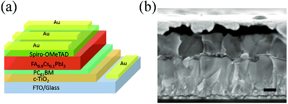 | ||
| Fig. 1 (a) Perovskite solar cell with the structure of FTO/compact TiO2/PCBM/perovskite/OMeTAD/Au. (b) SEM image of planar formamidinium perovskite solar cell. The scale bar is 200 nm. | ||
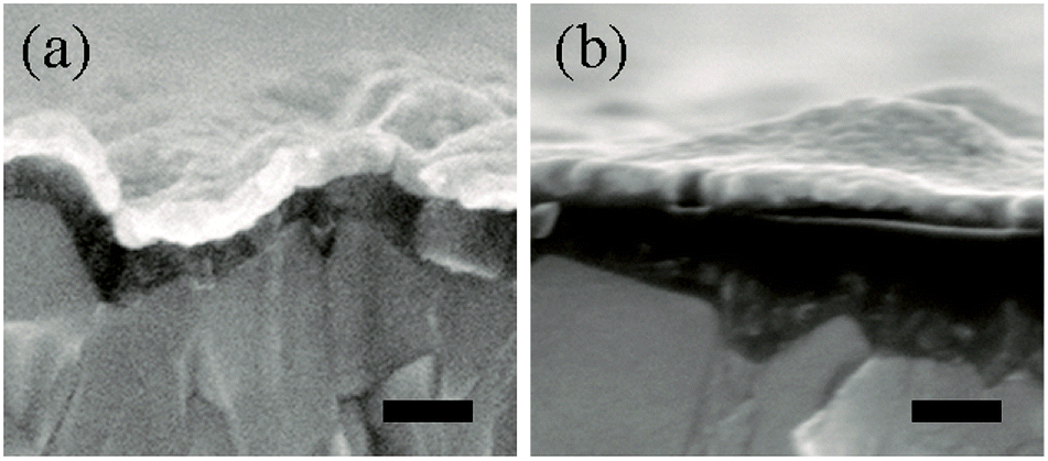 | ||
| Fig. 2 Cross-sectional SEM images of (a) TiO2 compact layer and (b) TiO2 compact layer with PCBM30 intermediate layer. Au capping layers are used for facilitating the SEM measurement. The scale bar is 100 nm. | ||
We study the effect of PCBM intermediate layers on the morphology of formamidinium perovskite layers by means of SEM measurements. Fig. 3a shows the morphology of the TiO2 electron transport layers as a reference. After depositing formamidinium perovskite without any intermediate layers, a compact perovskite layer is formed with an average grain size of 108 nm (Fig. 3b). By inserting PCBM intermediate layers at the TiO2/perovskite interfaces, a remarkable increase can be observed on the average grain size of formamidinium perovskite layers, namely, 206 nm, 230 nm, 302 nm, and 316 nm for the PCBM10, PCBM20, PCBM30 and PCBM40 intermediate layers (Fig. 3c–f), respectively. Therefore, PCBM intermediate layers facilitate the growth of formamidinium perovskite grains.
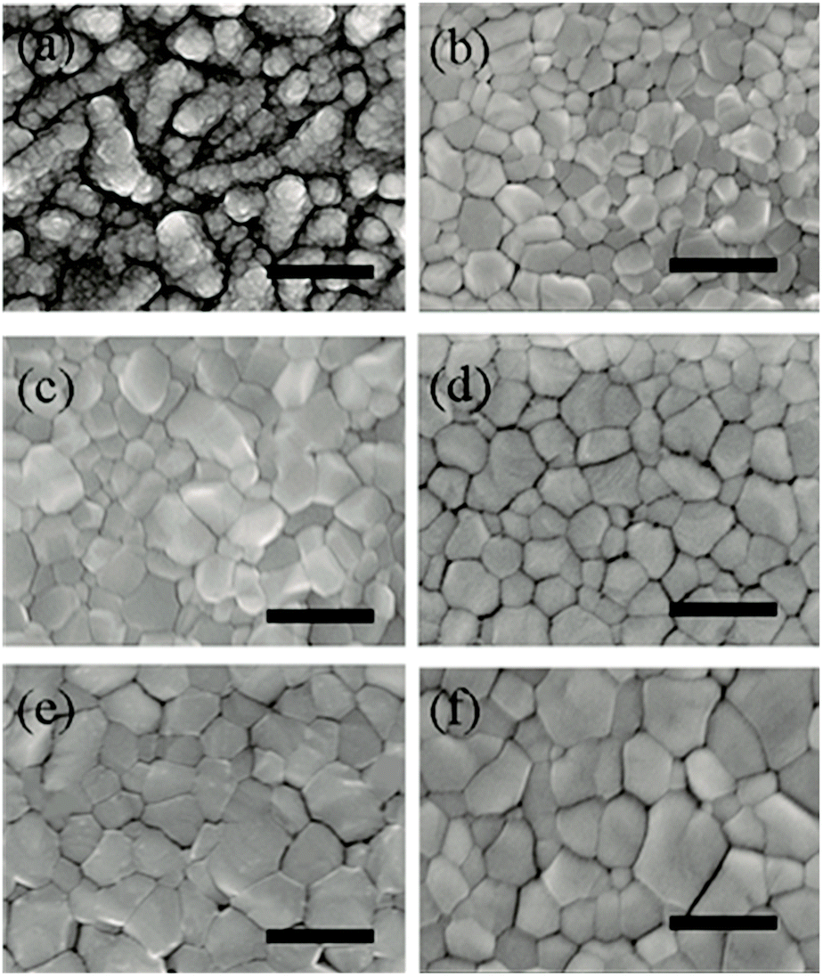 | ||
| Fig. 3 (a) Morphology of compact TiO2 layer on FTO substrate and morphology of perovskite films (b) without PCBM and with (c) PCBM10, (d) PCBM20, (e) PCBM30, and (f) PCBM40 intermediate layers. The scale bar is 500 nm. | ||
Fig. 4a shows the XRD patterns of formamidinium perovskite layers on different PCBM intermediate layers. Except three diffraction peaks from the FTO substrates, all the main diffraction peaks can be assigned to the trigonal crystal structure of formamidinium perovskite materials, which implies the successful deposition of α-phase formamidinium perovskite layers.32–34 It is also noted that a small diffraction peak at about 22.5° exists in the XRD pattern of the samples without PCBM intermediate layers. This peak can be assigned to the diffraction of the (002) planes in the yellow δ-phase of formamidinium perovskite materials.35,36 As the photovoltaic performance of the yellow δ-phase is much lower than that of the black α-phase, the yellow δ-phase is believed to be harmful to the solar-to-electric conversion process. It is also found that the diffraction peak of the yellow δ-phase can be eliminated by the PCBM intermediate layers with optimized precursor concentrations (PCBM20 and PCBM30). Therefore, PCBM intermediate layers have the function of inhibiting the formation of the yellow δ-phase. Furthermore, the full width at half maximum (FWHM) of the (110) diffraction peaks in these five samples are also different,37–41 which is summarized in Fig. 4b. The formamidinium perovskite layer on the TiO2-coated FTO substrate has the FWHM of 0.214°, which can be decreased by adding PCBM intermediate layers: the PCBM30 intermediate layer yields the smallest FWHM of 0.187°. Further increasing the concentration of the PCBM precursor solution to 40 mg mL−1 results in an increase of the FWHM to 0.201°. The broadening of the XRD peaks is usually induced by the low quality of crystallization. Then, the smallest FWHM of the formamidinium perovskite material with PCBM30 intermediate layer reflects its highest quality among these five samples.
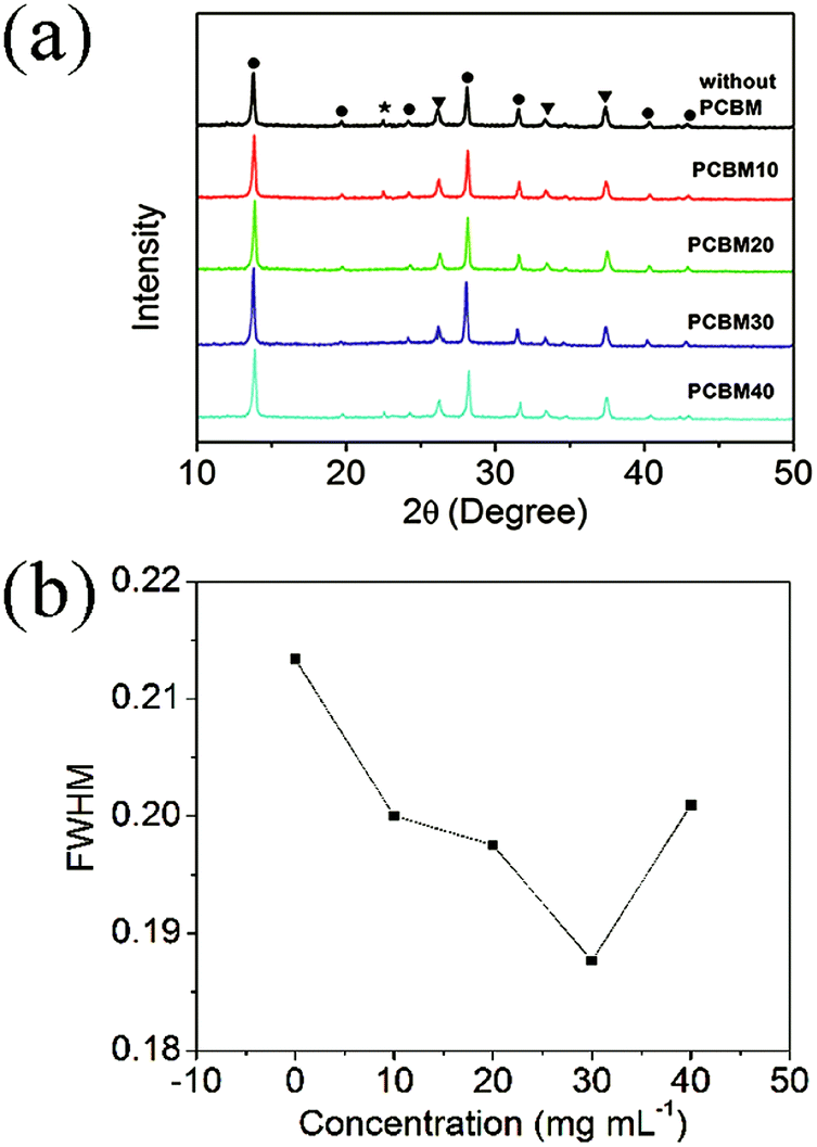 | ||
| Fig. 4 (a) XRD patterns of perovskite layers without and with different PCBM intermediate layers, and (b) the FWHM of the (110) diffraction peaks. The diffraction peaks of FTO, α-FA0.9Cs0.1PbI3, and its yellow δ-phase are labeled with triangles, circles and stars, respectively. | ||
As the PCBM intermediate layers change the surface of the substrates, the spin-coated PbI2 layers are subsequently modified, which can affect the formation of perovskite layers. The formation of yellow δ-phase comes from the low stability of the black α-phase in formamidinium lead iodide materials, which is related to the large tolerance factor of their perovskite crystal structure. The SEM and XRD measurements (Fig. 3 and 4, respectively) indicate that the PCBM intermediate layers can encourage the crystallization and growth of perovskite layers with the α-phase structure. It implies that the presence of PCBM facilities the formation of the black α-phase and improve its stability. We think that this is the possible reason for restraining the formation of the yellow δ-phase by the PCBM intermediate layers. The main interaction between PCBM and formamidinium perovskite is located at the vicinity of the TiO2/perovskite interface. Moreover, previous literatures have reported that PCBM can partially diffuse into the perovskite layers.42 Therefore, the interaction between PCBM and formamidinium perovskite can extend into the perovskite layers.
Fig. 5a shows the typical J–V curves of devices with different intermediate layers under one sun condition, and photovoltaic parameters are listed in Table S1.† The device without a PCBM intermediate layer shows poor performance with the power conversion efficiency (PCE) of 6.6%, open-circuit voltage (VOC) of 1.08 V, short-circuit current density (JSC) of 12.3 mA cm−2, and fill factor (FF) of 0.497. By inserting the PCBM10 intermediate layer, JSC and FF are remarkably increased to 16.7 mA cm−2 and 0.603, respectively. It is noted that the performance improvement is dependent on the concentration of PCBM precursor solutions. For the intermediate layers of PCBM20 and PCBM30, JSC and PCE of the devices increase with the increase of the PCBM concentration. Further increasing the concentration of PCBM solutions to 40 mg mL−1, JSC and PCE of the devices decrease to 18.1 mA cm−2 and 12.2%, respectively. For the optimized intermediate layer of PCBM30, the corresponding device has a PCE of 15.5% with JSC of 22.7 mA cm−2, photovoltage of 1.05 V, and FF of 0.653. Therefore, intermediate layers, which are fabricated by 30 mg mL−1 PCBM solution, can remarkably improve the performance of planar devices with formamidinium perovskite materials as the harvester. The improved performance of devices with PCBM30 layers is in accordance with the improvement of crystallization and elimination of the yellow δ-phase as evident from the SEM and XRD measurements. Fig. 5b shows the statistics of PCEs for 30 devices without intermediate layers and with PCBM30 intermediate layers. For the devices with PCBM30 intermediate layers, the average PCE is 15.1% and the highest PCE is 16.8%, which are obviously higher than those for devices without intermediate layers (6.8% and 8.7%, respectively). This result confirms the improvement of device performance by inserting PCBM30 intermediate layers. We fabricated formamidinium perovskite solar cells with mesoporous TiO2 layers for comparing the hysteresis effect with our planar devices. As shown in Fig. 5c, the mesoporous device gives remarkably different J–V curves between forward scan and reverse scan, while the planar device with PCBM30 intermediate layer has little difference on the J–V curves with opposite scan directions. Therefore, planar devices with PCBM30 intermediate layers eliminate the hysteresis effect, which usually exists in mesoporous perovskite solar cells.43
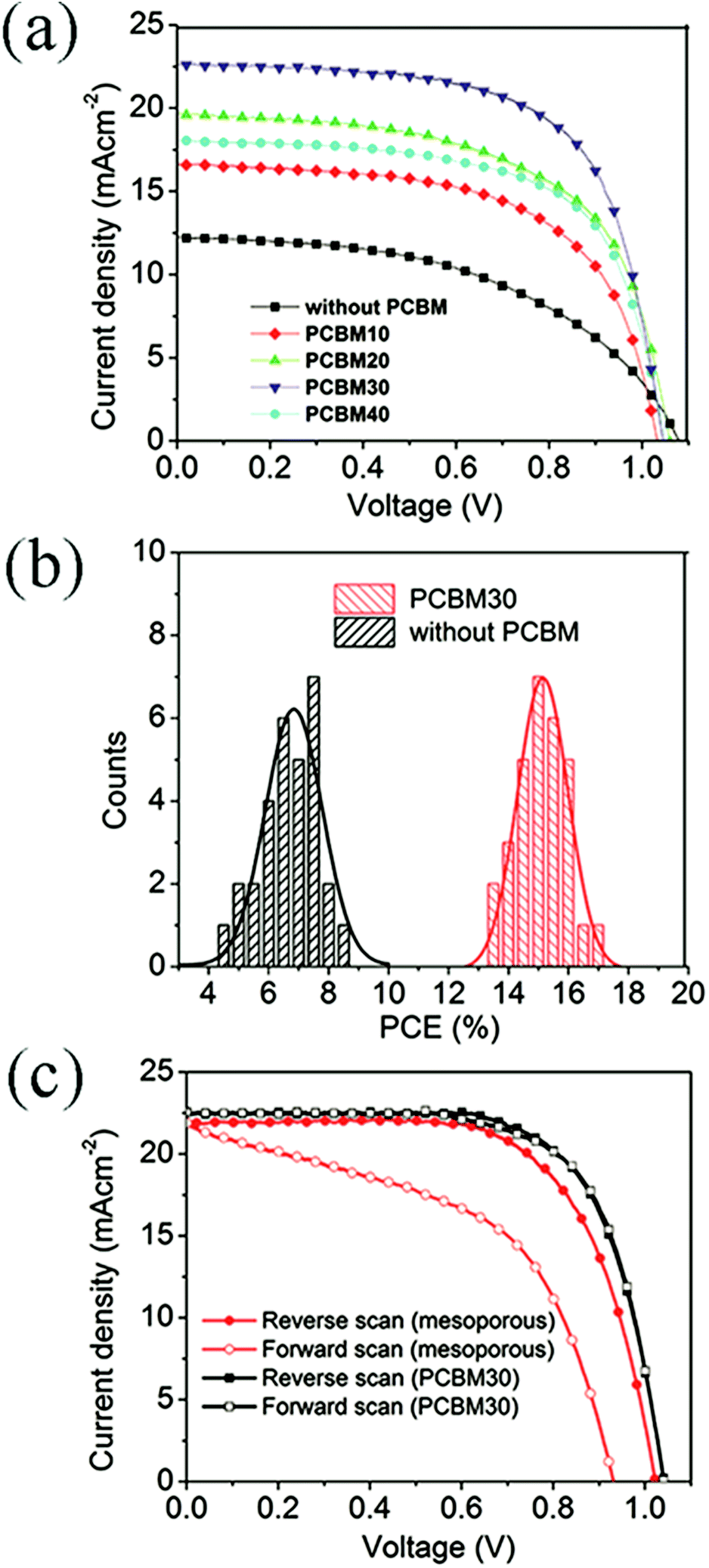 | ||
| Fig. 5 (a) Typical J–V curves of devices without and with different PCBM intermediate layers, (b) statistics of PCEs for 30 devices without and with PCBM30 intermediate layers, and (c) J–V curves of mesoporous device and planar device with PCBM30 intermediate layer under both forward and reverse scans. | ||
PL spectrum is a facile tool for characterizing the charge transfer at TiO2/perovskite interfaces.42,44 Fig. 6 shows the PL spectra of formamidinium perovskite layers on TiO2-coated substrates without and with different PCBM intermediate layers, and the formamidinium perovskite layer on the glass substrate without a TiO2 layer is used as the reference. For the sample without intermediate layers, the intensity of the PL peak quenches to 7.8% of the intensity of the reference sample, which reflects the intensive extraction of photoelectrons from perovskite layers to TiO2 layers. By inserting PCBM10 intermediate layers between TiO2 layers and perovskite layers, the intensity of PL peaks increases to 13.8% of the intensity of the reference sample, and the quenching effect of the PL peak slightly attenuates. By increasing the concentration of PCBM solutions, the quenching effect of the PL peak continuously decreases. This result means that PCBM intermediate layers cannot improve the charge transfer process at the interface between the TiO2 layers and formamidinium perovskite layers.
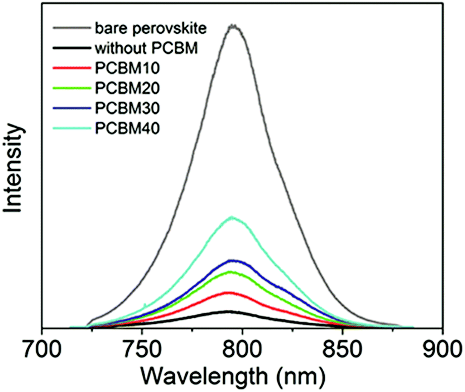 | ||
| Fig. 6 PL spectra of the perovskite layer on a glass substrate and perovskite layers on TiO2 compact layers without and with PCBM10, PCBM20, PCBM30, and PCBM40 intermediate layers. | ||
To reveal the function of PCBM intermediate layers in formamidinium perovskite solar cells, we perform impedance measurements at 0.7 V bias potential under constant light illumination. Fig. 7 shows the Nyquist plots of the devices without and with different PCBM intermediate layers. In the Nyquist plots, two impedance arches can be distinguished. As discussed in previous reports, the high-frequency arch can be attributed to the charge transfer process at the TiO2/perovskite interface, and the low-frequency arch is attributable to the recombination process in the perovskite layers.45,46 By fitting the impedance data with an equivalent circuit (Fig. 7), we can extract the charge transfer resistance (Rct) and recombination resistance (Rrec), which are listed in Table S2.† Rct of the device without an intermediate layer is 3.7 Ω cm2, and it increases after inserting PCBM intermediate layers in the devices. For PCBM10, PCBM20, and PCBM30 intermediate layers, Rct gradually increases from 22.0 Ω cm2 to 29.6 Ω cm2 and 40.0 Ω cm2, respectively. It is noted that Rct remarkably increases to 706.4 Ω cm2 for the device with the PCBM40 intermediate layer. This increase of Rct reflects the slow charge transfer process at the TiO2/perovskite interface. It means that PCBM intermediate layers cannot promote the charge transfer process, and PCBM40 layer intensively blocks the charge transfer process. This result is in accordance with the analysis of the PL spectra (Fig. 6). On the other hand, Rrec of the device without an intermediate layer is 40.3 Ω cm2, which increases after the PCBM intermediate layers are inserted. For PCBM10, PCBM20, and PCBM30, Rrec remarkably increases up to 631.7 Ω cm2, 839.2 Ω cm2, and 1236.3 Ω cm2, respectively. After further increasing the concentration of the precursor solution to 40 mg mL−1, Rrec of the devices slightly decreases to 1215.4 Ω cm2. As large Rrec is related with a slow recombination process in the perovskite layers, PCBM layers remarkably reduce the recombination process. This is in accordance with the promotion of crystallization and elimination of the yellow δ-phase in the SEM and XRD measurements by inserting PCBM intermediate layers. As PCBM30 intermediate layers have relative small Rct and large Rrec, the corresponding devices yield optimized PCE. The decrease of PCE in devices with PCBM40 intermediate layers should be attributed to the remarkable increase of Rct, which blocks the charge extraction process at TiO2/perovskite interfaces.
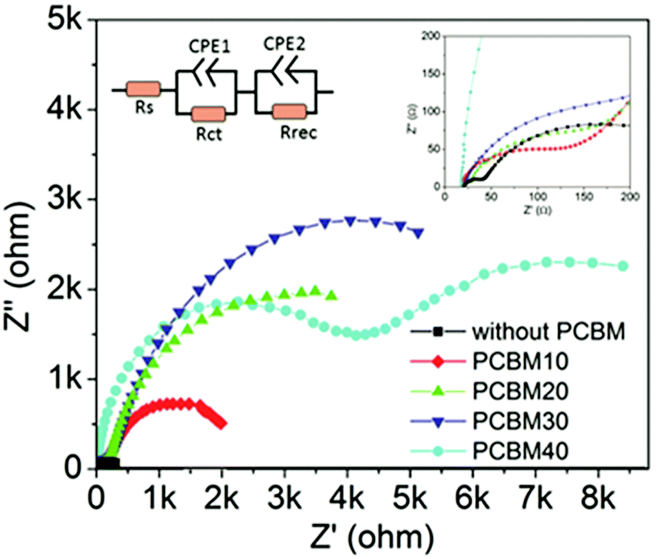 | ||
| Fig. 7 Nyquist plots of devices without and with different PCBM intermediate layers measured at a bias voltage of 0.7 V under constant illumination. Top-right corner is the enlargement of the high-frequency arches. | ||
Conclusions
In summary, we have fabricated efficient planar junction solar cells with formamidinium perovskite as the light harvester by a two-step method, and the functions of PCBM intermediate layers are investigated. The SEM images indicate that PCBM intermediate layers improve the growth of perovskite grains, and the XRD patterns show that PCBM layers improve the crystallization and eliminate the yellow δ-phase in formamidinium perovskite layers. It is found that the function of PCBM intermediate layers is dependent on the concentration of precursor solutions. By using optimized PCBM intermediate layers, the average PCE of planar devices can be increased from 6.8% to 15.1%, and the J–V curves of optimized devices show a marginal hysteresis effect. The impedance and PL measurements indicate that PCBM layers remarkably reduce the recombination process in formamidinium perovskite layers, but thick PCBM layers block the charge transfer process at TiO2/perovskite interfaces. The optimized condition comes from the balance between these two effects.Acknowledgements
This work was partially supported by National Natural Science Foundation of China (Grant no. 51273079, 11374121) and the Science Development Program of Jilin Province (Grant no. 20150519021JH).References
- A. Kojima, K. Teshima, Y. Shirai and T. Miyasaka, J. Am. Chem. Soc., 2009, 131, 6050–6051 CrossRef CAS PubMed.
- J. Im, C. Lee, J. Lee, S. Park and N. Park, Nanoscale, 2011, 3, 4088–4093 RSC.
- H. Kim, C. Lee, J. Im, K. Lee, T. Moehl, A. Marchioro, S. Moon, R. Humphry-Baker, J. Yum, J. Moser, M. Grätzel and N. Park, Sci. Rep., 2012, 2, 591–597 Search PubMed.
- M. Lee, J. Teuscher, T. Miyasaka, T. Murakami and H. Snaith, Science, 2012, 338, 643–648 CrossRef CAS PubMed.
- C. Stoumpos, C. Malliakas and M. Kanatzidis, Inorg. Chem., 2013, 52, 9019–9038 CrossRef CAS PubMed.
- J. Lee, D. Seol, A. Cho and N. Park, Adv. Mater., 2014, 26, 4991–4998 CrossRef CAS PubMed.
- G. Eperon, S. Stranks, C. Menelaou, M. Johnston, L. Herz and H. Snaith, Energy Environ. Sci., 2014, 7, 982–988 CAS.
- N. Pellet, P. Gao, G. Gregori, T. Yang, M. Nazeeruddin, J. Maier and M. Grätzel, Angew. Chem., Int. Ed., 2014, 53, 3151–3157 CrossRef CAS PubMed.
- W. Yang, J. Noh, N. Jeon, Y. Kim, S. Ryu, J. Seo and S. Seok, Science, 2015, 348, 1234–1237 CrossRef CAS PubMed.
- N. Jeon, J. Noh, W. Yang, Y. Kim, S. Ryu, J. Seo and S. Seok, Nature, 2015, 517, 476–480 CrossRef CAS PubMed.
- Y. Zhang, J. Wang, J. Xu, W. Chen, D. Zhu, W. Zheng and X. Bao, RSC Adv., 2016, 6, 79952–79957 RSC.
- J. Heo, H. Han, D. Kim, T. Ahn and S. Im, Energy Environ. Sci., 2015, 8, 1602–1608 CAS.
- Q. Wei, D. Yang, Z. Yang, X. Ren, Y. Liu, J. Feng, X. Zhu and S. Liu, RSC Adv., 2016, 6, 56807–56811 RSC.
- A. Binek, F. Hanusch, P. Docampo and T. Bein, J. Phys. Chem. Lett., 2015, 6, 1249–1253 CrossRef CAS PubMed.
- N. Jeon, J. Noh, W. Yang, Y. Kim, S. Ryu, J. Seo and S. Seok, Nature, 2015, 517, 476–480 CrossRef CAS PubMed.
- T. Koh, K. Fu, Y. Fang, S. Chen, T. Sum, N. Mathews, S. Mhaisalkar, P. Boix and T. Baikie, J. Phys. Chem. C, 2014, 118, 16458–16462 CAS.
- D. Luo, L. Zhao, J. Wu, Q. Hu, Y. Zhang, Z. Xu, Y. Liu, T. Liu, K. Chen, W. Yang, W. Zhang, R. Zhu and Q. Gong, Adv. Mater., 2017, 1604758 CrossRef PubMed.
- S. Yang, W. Liu, L. Zuo, X. Zhang, T. Ye, J. Chen, C. Li, G. Wu and H. Chen, J. Mater. Chem. A, 2016, 4, 9430–9436 CAS.
- C. Wu, C. Chiang, Z. Tseng, M. Nazeeruddin, A. Hagfeldt and M. Grätzel, Energy Environ. Sci., 2015, 8, 2725–2733 CAS.
- H. Ko, J. Lee and N. Park, J. Mater. Chem. A, 2015, 3, 8808–8815 CAS.
- D. Seol, J. Lee and N. Park, ChemSusChem, 2015, 8, 2414–2419 CrossRef CAS PubMed.
- Z. Zhou, S. Pang, Z. Liu, H. Xu and G. Cui, J. Mater. Chem. A, 2015, 3, 19205–19217 CAS.
- R. Wu, B. Yang, C. Zhang, Y. Huang, Y. Cui, P. Liu, C. Zhou, Y. Hao, Y. Gao and J. Yang, J. Phys. Chem. C, 2016, 120, 6996–7004 CAS.
- C. Wang and J. Yang, Sci. China Mater., 2016, 59, 743–756 CrossRef.
- Y. Li, Y. Zhao, Q. Chen, Y. Yang, Y. Liu, Z. Hong, Z. Liu, Y. Hsieh, L. Meng, Y. Li and Y. Yang, J. Am. Chem. Soc., 2015, 137, 15540–15547 CrossRef CAS PubMed.
- T. Ma, D. Tadaki, M. Sakuraba, S. Sato, A. Hirano-Iwata and M. Niwano, J. Mater. Chem. A, 2016, 4, 4392–4397 CAS.
- Y. Dong, W. Li, X. Zhang, Q. Xu, Q. Liu, C. Li and Z. Bo, Small, 2016, 12, 1098–1104 CrossRef CAS PubMed.
- Z. Zhou, J. Xu, L. Xiao, J. Chen, Z. Tan, J. Yao and S. Dai, RSC Adv., 2016, 6, 78585–78594 RSC.
- C. Tao, S. Neutzner, L. Colella, S. Marras, A. Kandada, M. Gandini, M. Bastiani, G. Pace, L. Manna, M. Caironi, C. Bertarelli and A. Petrozza, Energy Environ. Sci., 2015, 8, 2365–2370 CAS.
- S. Yuan, Z. Qiu, H. Zhang, X. Qiu, C. Gao, H. Gong, S. Yang, J. Yu and B. Cao, RSC Adv., 2016, 6, 47459–47467 RSC.
- X. Xia, W. Wu, H. Li, B. Zheng, Y. Xue, J. Xu, D. Zhang, C. Gao and X. Liu, RSC Adv., 2016, 6, 14792–14798 RSC.
- J. Lee, D. Kim, H. Kim, S. Seo, S. Cho and N. Park, Adv. Energy Mater., 2015, 5, 1501310 CrossRef.
- Y. Zhang, J. Wang, J. Xu, W. Chen, D. Zhu, W. Zheng and X. Bao, RSC Adv., 2016, 6, 79952–79957 RSC.
- C. Yi, J. Luo, S. Meloni, A. Boziki, N. Ashari-Astani, C. Grätzel, S. Zakeeruddin, U. Röthlisberger and M. Grätzel, Energy Environ. Sci., 2016, 9, 656–662 CAS.
- Q. Han, S. Bae, P. Sun, Y. Hsieh, Y. Yang, Y. Rim, H. Zhao, Q. Chen, W. Shi, G. Li and Y. Yang, Adv. Mater., 2016, 28, 2253–2258 CrossRef CAS PubMed.
- Y. Fu, H. Zhu, A. Schrader, D. Liang, Q. Ding, P. Joshi, L. Hwang, X. Zhu and S. Jin, Nano Lett., 2016, 16, 1000–1008 CrossRef CAS PubMed.
- D. Yuan, A. Gorka, M. Xu, Z. Wang and L. Liao, Phys. Chem. Chem. Phys., 2015, 17, 19745–19750 RSC.
- Z. Li, M. Yang, J. Park, S. Wei, J. Berry and K. Zhu, Chem. Mater., 2016, 28, 284–292 CrossRef CAS.
- W. Nie, H. Tsai, R. Asadpour, J. Blancon, A. Neukirch, G. Gupta, J. Crochet, M. Chhowalla, S. Tretiak, M. Alam, H. Wang and A. Mohite, Science, 2015, 347, 522–525 CrossRef CAS PubMed.
- M. Gangishetty, R. Scott and T. Kelly, Nanoscale, 2016, 8, 6300–6307 RSC.
- W. Ke, C. Xiao, C. Wang, B. Saparov, H. Duan, D. Zhao, Z. Xiao, P. Schulz, S. Harvey, W. Liao, W. Meng, Y. Yu, A. Cimaroli, C. Jiang, K. Zhu, M. Al-Jassim, G. Fang, D. Mitzi and Y. Yan, Adv. Mater., 2016, 28, 5214–5221 CrossRef CAS PubMed.
- Y. Shao, Z. Xiao, C. Bi, Y. Yuan and J. Huang, Nat. Commun., 2014, 5, 5784 CrossRef CAS PubMed.
- N. Elumalai and A. Uddin, Sol. Energy Mater. Sol. Cells, 2016, 157, 476–509 CrossRef CAS.
- M. Cai, V. Tiong, T. Hreid, J. Bell and H. Wang, J. Mater. Chem. A, 2015, 3, 2784–2793 CAS.
- E. Juarez-Perez, M. Wuβler, F. Fabregat-Santiago, K. Lakus-Wollny, E. Mankel, T. Mayer, W. Jaegermann and I. Mora-Sero, J. Phys. Chem. Lett., 2014, 5, 680–685 CrossRef CAS PubMed.
- J. Zhang, E. Juárez-Pérez, I. Mora-Seró, B. Viana and T. Pauporté, J. Mater. Chem. A, 2015, 3, 4909–4915 CAS.
Footnote |
| † Electronic supplementary information (ESI) available. See DOI: 10.1039/c7ra04311b |
| This journal is © The Royal Society of Chemistry 2017 |