
 Open Access Article
 This Open Access Article is licensed under a Creative Commons Attribution-Non Commercial 3.0 Unported Licence
Lead-free and amorphous organic–inorganic hybrid materials for photovoltaic applications: mesoscopic CH3NH3MnI3/TiO2 heterojunction†
Xianxi Zhang*a,
Jie Yina,
Zhonghao Niea,
Qian Zhanga,
Ning Suib,
Baoli Chena,
Yingtian Zhanga,
Konggang Qua,
Jinsheng Zhaoa and
Huawei Zhou *a
*a
aShandong Provincial Key Laboratory of Chemical Energy Storage and Novel Cell Technology, School of Chemistry and Chemical Engineering, Liaocheng University, College of Materials Science and Engineering, Liaocheng 252059, China. E-mail: zhouhuaweiopv@163.com; xxzhang3@126.com
bCollege of Materials Science and Engineering, Qingdao University of Science and Technology, Qingdao 266042, China
First published on 28th July 2017
Abstract
As one type of organic–inorganic hybrid material, APbX3 organic–inorganic lead perovskite materials have attracted considerable attention in optoelectronic applications. Although organic–inorganic lead perovskites possess high solar-to-electrical conversion efficiency, the toxic Pb in organic–inorganic lead perovskites is expected to cause environmental pollution in future mass applications. Thus, exploiting Pb-free organic–inorganic hybrid materials is urgently needed. In this study, a lead-free and amorphous CH3NH3MnI3 (a-MAMnI3) thin film was prepared by spin coating a mixed MnI2 and MAI precursor solution on an electronic transport layer (ETL)-TiO2. A mesoscopic a-MAMnI3/TiO2 heterojunction was formed by filling the mesoporous TiO2 layer with MAMnI3. The architecture of the optoelectronic device is FTO/ETL-TiO2/a-MAMnI3/Spiro-MeOTAD/Ag. The photovoltage of the optoelectronic device based on the mesoscopic a-MAMnI3/TiO2 heterojunction reached 300 mV under AM1.5, 100 mW cm−2 simulated illumination. The evident photoresponse was observed at 530 nm green light. The test with 2000 s on/off cycling indicated the good stability and repeatability of the device. The findings pave a way for realizing Pb-free and amorphous organic–inorganic hybrid materials applied to optoelectronic logic devices, photodetectors, and optical memory devices.
Introduction
Organic–inorganic hybrid materials have attracted significant attention as functional layers for optoelectronic applications1 because of their superior charge carrier mobility for inorganic semiconductors and their solution processability.2 At present, organic–inorganic hybrid materials present promising performance in solar cells,3 field-effect transistors,4 light-emitting diodes,5 upconversion emission,6 and so on. Notably, as one type of organic–inorganic hybrid material, ABX3 organic–inorganic perovskite materials have received serious consideration all over the world because of the high solar-to-electrical conversion efficiency of organic–inorganic perovskite solar cells. Since 2012, the solar-to-electrical conversion efficiency of organic–inorganic lead (Pb) perovskites has increased from 3.9% (ref. 7) to 21%,8 which is close to that of commercial silicon solar cells.Although organic–inorganic lead perovskites possess high solar-to-electrical conversion efficiency,8 tunable bandgap,9,10 high carrier mobility,11,12 and low exciton binding energy (14–25 meV),13,14 many problems remain, and they include stability,15,16 reproducibility,8,17 and anomalous hysteresis.18,19 Furthermore, the toxic Pb content of organic–inorganic lead perovskites is expected to cause environmental pollution in future mass applications. Thus, exploiting new substitutes for organic–inorganic Pb perovskites is urgently needed. In recent years, a number of groups, including the authors of the present work, have focused on developing and investigating Pb-free organic–inorganic hybrid materials, including MASnI3,20,21 AGeI3 (A = Cs, MA, or FA),22 and MA2MnCl4.23 However, Ge and Sn are easily oxidized, leading to device degradation. Organic–inorganic (manganese) hybrid materials, such as (pyrrolidinium)MnCl3,24 [(CH3)2NH2]Mn(HCOO)3,25 MA2MnCl4,23 [Mn2(BPTCA)(phen)2·H2O]n,26 and Mn(C6H8O4)(H2O),27 have been developed into various functional materials for ferroelectricity,26 luminescence,24 photocatalysis28 and magnetic applications.29 In our previous report, incarnate MA2MnCl4 presented ultraviolet photoresponse.23 If halide is changed in MA2MnCl4, then the optical bandgap may be tuned and device performance may be improved. With the aforementioned motivation, we aim to investigate the photoresponse of MAMnI3 thin films for opto-electronic applications.
In this study, a Pb-free and amorphous MAMnI3 (a-MAMnI3) thin film was prepared by spin coating mixed MnI2 and MAI precursor solution on an electronic transport layer (ETL)-TiO2. Mesoscopic a-MAMnI3/TiO2 heterojunction was formed by filling the mesoporous TiO2 layer with a-MAMnI3. The architecture of the optoelectronic device comprised FTO/ETL-TiO2/a-MAMnI3/Spiro-MeOTAD/Ag. The photovoltage of the optoelectronic device based on the a-MAMnI3 film reached 300 mV under AM1.5, 100 mW cm−2 simulated illumination.
Compared with MA2MnCl4 materials exhibiting ultraviolet photoresponse, the a-MAMnI3-based device presented obvious photoresponse not only to ultraviolet light but also to visible light. The evident photoresponse was observed at 530 nm green light. Finally, the test with 2000 s on/off cycling indicated the good stability and repeatability of the device.
Experimental section
Synthesis of MAI
MAI was synthesized following our previous report.30Fabrication and characterizations of FTO/ETL-TiO2/a-MAMnI3/Spiro-MeOTAD/Ag devices
Patterned FTO-coated glass substrates with a sheet resistance of 15 Ω sq−1 were coated with a TiO2 compact layer by spin-coating the TiO2 organic sol at 3000 rpm. for 30 s, followed by drying at 450 °C for 30 minutes, following our previous literature.31 The mesoporous TiO2 layer was coated with a commercial TiO2 paste (Dyesol 18NRT, Dyesol) diluted in ethanol (1![[thin space (1/6-em)]](https://www.rsc.org/images/entities/char_2009.gif) :3.5, weight ratio) by spin coating at 5000 rpm. for 30 s, followed by gradually heated to 500 °C, baked at this temperature for 30 min. The a-MAMnI3 layer was prepared by spin coating a mixed precursor solution comprising 1.0 mol L−1 MnI2 and 1.0 mol L−1 MAI on ETL-TiO2. At 3000 rpm. for 30 s, followed by gradually heated to 100 °C, baked at this temperature for 30 min. The Spiro-MeOTAD hole transport material (HTM) were spin-coated on FTO/ETL-TiO2/MAMnI3 substrate at 3000 rpm for 30 s using HTMs/1,2-dichlorobenzene (72.3 mg mL−1) with 17.5 μL Li-bis(trifluoromethanesulfonyl)imide (Li-TFSI)/acetonitrile (28.3 mg mL−1), 29 μL tris(2-(1H-pyrazol-1-yl)-4-tert-butylpyridine) cobalt(III) bis(trifluoromethylsulphonyl)imide and 28.8 μL TBP as additives. Finally, silver (50 nm) was vacuum deposited on top of the device to form the back contact. Nanostructures of films and devices were characterized by scanning electron microscopy (SEM, Hitachi SEM S-4800). UV-vis absorption spectrum was obtained using UV/vis/NIR spectrometer (Perkinelmer, lambda, 750S). The photocurrent–voltage performances of the device with 0.12 cm2 photoelectrode were measured by a Keithley digital source meter (Keithley 2400, USA) and equipped with a solar simulator (IV5, PV Measurements, Inc., USA). The photocurrent–time performance of the device was carried out by an electrochemical workstation system (CHI760, Chenhua, and Shanghai) and equipped with a solar simulator (IV5, PV Measurements, Inc., USA). The photocurrent–time with incident photon (wavelength) and frequency response were measured by an electrochemical workstation system (CHI760, Chenhua, and Shanghai) and equipped with a quantum efficiency/spectral response (SR)/incident photon to current conversion efficiency (IPCE) measurement system (QEX10, PV Measurements, Inc., USA).
:3.5, weight ratio) by spin coating at 5000 rpm. for 30 s, followed by gradually heated to 500 °C, baked at this temperature for 30 min. The a-MAMnI3 layer was prepared by spin coating a mixed precursor solution comprising 1.0 mol L−1 MnI2 and 1.0 mol L−1 MAI on ETL-TiO2. At 3000 rpm. for 30 s, followed by gradually heated to 100 °C, baked at this temperature for 30 min. The Spiro-MeOTAD hole transport material (HTM) were spin-coated on FTO/ETL-TiO2/MAMnI3 substrate at 3000 rpm for 30 s using HTMs/1,2-dichlorobenzene (72.3 mg mL−1) with 17.5 μL Li-bis(trifluoromethanesulfonyl)imide (Li-TFSI)/acetonitrile (28.3 mg mL−1), 29 μL tris(2-(1H-pyrazol-1-yl)-4-tert-butylpyridine) cobalt(III) bis(trifluoromethylsulphonyl)imide and 28.8 μL TBP as additives. Finally, silver (50 nm) was vacuum deposited on top of the device to form the back contact. Nanostructures of films and devices were characterized by scanning electron microscopy (SEM, Hitachi SEM S-4800). UV-vis absorption spectrum was obtained using UV/vis/NIR spectrometer (Perkinelmer, lambda, 750S). The photocurrent–voltage performances of the device with 0.12 cm2 photoelectrode were measured by a Keithley digital source meter (Keithley 2400, USA) and equipped with a solar simulator (IV5, PV Measurements, Inc., USA). The photocurrent–time performance of the device was carried out by an electrochemical workstation system (CHI760, Chenhua, and Shanghai) and equipped with a solar simulator (IV5, PV Measurements, Inc., USA). The photocurrent–time with incident photon (wavelength) and frequency response were measured by an electrochemical workstation system (CHI760, Chenhua, and Shanghai) and equipped with a quantum efficiency/spectral response (SR)/incident photon to current conversion efficiency (IPCE) measurement system (QEX10, PV Measurements, Inc., USA).
Results and discussions
Solution-processed optoelectronic devices are cost effective to manufacture and offer physical flexibility. Perovskite nanopigments are notably easy to prepare and deposit through simple solution processing via spin coating or dip coating. The preparation process of ETL-TiO2/a-MAMnI3 thin films is shown in Fig. 1. The preparation process of ETL-TiO2, including a compact layer and mesoporous TiO2 layer, is described in our previous report.31 ETL-TiO2 was colorless and transparent. The yellow film was formed after spin coating a mixed precursor solution comprising 1.0 mol L−1 MnI2 and 1.0 mol L−1 MAI on ETL-TiO2. The film was labelled as MAI/MnI2 film. After heating on a hot plate at 100 °C, the yellow MAI/MnI2 film became a dark brown film, which was labelled as a-MAMnI3 film. The UV-vis absorption spectra were used to investigate the aforementioned absorption properties of the thin film. FTO/ETL-TiO2 films exhibit an absorption peak at 400 nm. The absorption intensity of the ultraviolet region increases from 300 nm to 355 nm, whereas the weak absorption intensity ranges from 450 nm to 800 nm. The absorption intensity of MAI/MnI2 thin films was slightly stronger than that of FTO/ETL-TiO2 films. The UV-vis absorption intensity of a-MAMnI3 was significantly enhanced.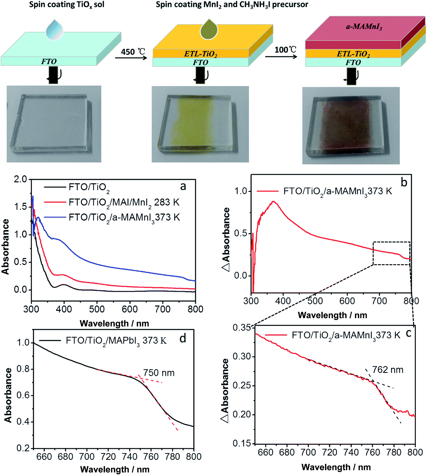 | ||
| Fig. 1 Schematics of the solution-processed TiO2 electronic transport layer (ETL) and a-MAMnI3 thin film. (a) UV-vis absorption spectrum of FTO/TiO2, FTO/TiO2/MAI/MnI2 283 K and FTO/TiO2/a-MAMnI3 373 K; (b) difference absorption between FTO/TiO2/a-MAMnI3 373 K and FTO/TiO2; (c) amplified plot from 650 nm to 800 nm of (c); (d) UV-vis absorption spectrum of FTO/TiO2/a-MAPbI3 373 K. | ||
The difference absorbance (ΔAbsorbance) between the absorbance of FTO/ETL-TiO2/a-MAMnI3 and FTO/ETL-TiO2 is shown in Fig. 1b and c. The a-MAMnI3 film presented a distinct absorption peak at 370 nm and an absorption edge at 762 nm. The classic MAPbI3 perovskite material shows an absorption edge at 750 nm (Fig. 1d) because the absorption edge is directly related to the bandgap. The result indicates that the bandgap of the a-MAMnI3 film was similar to that of MAPbI3. However, the absorption intensity of a-MAMnI3 was not as strong as that of MAPbI3 perovskite, hence the low photoelectric response in the succeeding results. In order to determine the phase structure of MAMnI3, we carried out the XRD test. The result was shown in Fig. S1 in (ESI†). Compared with FTO/TiO2, no new diffraction peaks was observed for MAI/MnI2 films films after heat treatment, which indicated that films were amorphous films. In addition, the thin film was prepared by spin coating a mixed precursor solution comprising MnI2 and MAI with mole ratio 1:1, followed by gradually heated to 100 °C to evaporating solvent. Thus, the thin film can be named amorphous MAMnI3. We can decide the organic–inorganic perovskite structure simply through the tolerance factor (t), t = (rA + rX)/[(21/2 (rB + rX))], where rA, rB, and rX are the onic radii of A, B, and X, respectively. The ionic radius of Pb2+ and Mn2+ are 119 and 80 pm, respectively. Thus, the value of tolerance factor for MAMnI3 is 0.94. The value of tolerance factor for MAPbI3 is 0.834. The reason for why the crystalline MAMnI3 cannot form may be high tolerance factor (t) and short bond length of Mn–I in MnI6−.
Scanning electron microscopy (SEM) was performed to study the micro-morphology of the thin films. The mesoporous TiO2 layer presented a mesoporous distribution (Fig. 2a), which favored increases in the adsorption capacity of the sensitizer and in photoelectric response efficiency. The surface morphology of a-MAMnI3 on the mesoporous TiO2 layer is shown in Fig. 2b to determine whether a-MAMnI3 is embedded into the mesoporous TiO2 layer. The figure shows that the a-MAMnI3 precursor solution is indeed embedded in the mesoporous TiO2 layer. Some islands were formed by the excess a-MAMnI3 precursor solution on the mesoporous TiO2 layer. In addition, the mesoporous TiO2 layer was not completely covered with the a-MAMnI3 film. This condition was expected to cause short-circuit contact between the ETL-TiO2 and the hole transport layer, increase electron recombination, and weaken the photoelectric performance. The reason of the mesoporous TiO2 not completed covered with the a-MAMnI3 film is that infiltration of the precursor solution on the TiO2 film is not good. In fact, we have made some improvement measures to improve coverage, such as increasing temperature of the precursor and TiO2 thin film to improve coverage. However, coverage has not improved significantly. In addition, the solvent and deposition method will also affect the coverage. In the future study, we will intend to change the solvent DMF to γ-butyrolactone, or prepare the a-MAMnI3 film by sequential deposition method. The surface element distribution of the a-MAMnI3 film was measured via EDS in SEM, as shown in Fig. 2c. The results show that the element distribution of Mn, I, C, and N in the micro-region is uniform.
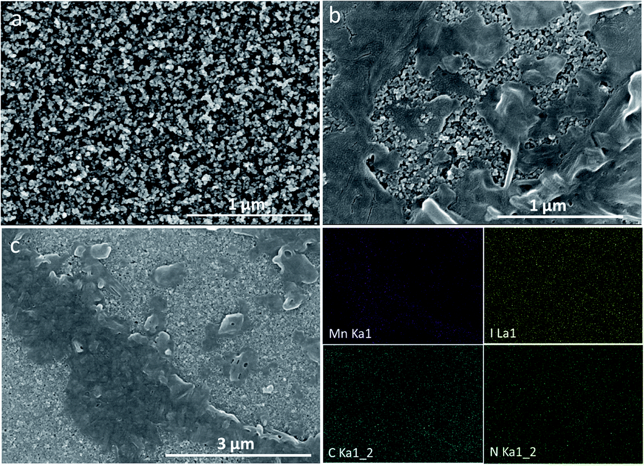 | ||
| Fig. 2 (a) SEM images of ETL (electronic transport layer)-TiO2 on FTO; (b) SEM images of a-MAMnI3 layer on ETL-TiO2; (c) energy dispersive X-ray spectra (EDS) mapping of each element for a-MAMnI3 layer on ETL-TiO2. | ||
The preparation process of the optoelectronic devices is shown in Fig. 3. The bandgap of the a-MAMnI3 thin film was close to that of MAPbI3; hence, a p-type hole transport material, Spiro-MeOTAD, was spin-coated on the a-MAMnI3 film. Then, back-electrode Ag was prepared via vacuum thermal evaporation. The architecture of the optoelectronic device comprised FTO/ETL-TiO2/a-MAMnI3/Spiro-MeOTAD/Ag. The cross section SEM of the device is shown in Fig. 3a. The thicknesses of the FTO, dense layer, and metal electrode layer were 398, 34, 48 nm, respectively. The dense layer of TiO2 showed uninterrupted coverage, which facilitates effective block hole injection.32 The MAI/MnI2 precursor is soluble in polar organic solvents, such as N,N-dimethylformamide. Therefore, it is solution processable and can be transformed into TiO2 pores at a molecular level to realize close contacts. The cross-sectional SEM image demonstrates that the Mesoscopic a-MAMnI3/TiO2 heterojunction was indeed formed with the filling of a-MAMnI3 into the mesoporous TiO2 layer. Initially, the photoelectric performance of FTO/ETL-TiO2/a-MAMnI3/Spiro-MeOTAD/Ag was obtained under AM1.5, 100 mW cm−2 simulated illumination. The best performance under open circuit voltage of 330 mV, short-circuit current density of 15.8 μA cm−2, filling factor of 0.41 and power conversion efficiency of 0.02% is presented in Fig. 3b. The photoelectric performance based on a-MAMnI3 was obviously better than that based on MA2MnCl4. The on/off photoelectric response is shown in Fig. 3c and d. When the simulated illumination was switched off, the current density remained at 0 μA cm−2 for about 10 s. When the simulated illumination was switched on, the current density instantaneously increased to about 2.4 μA cm−2. The maximum photocurrent density and the minimum photocurrent density of the device were almost unchanged after 2000 s cycling. This result indicated the good stability and repeatability of the device.
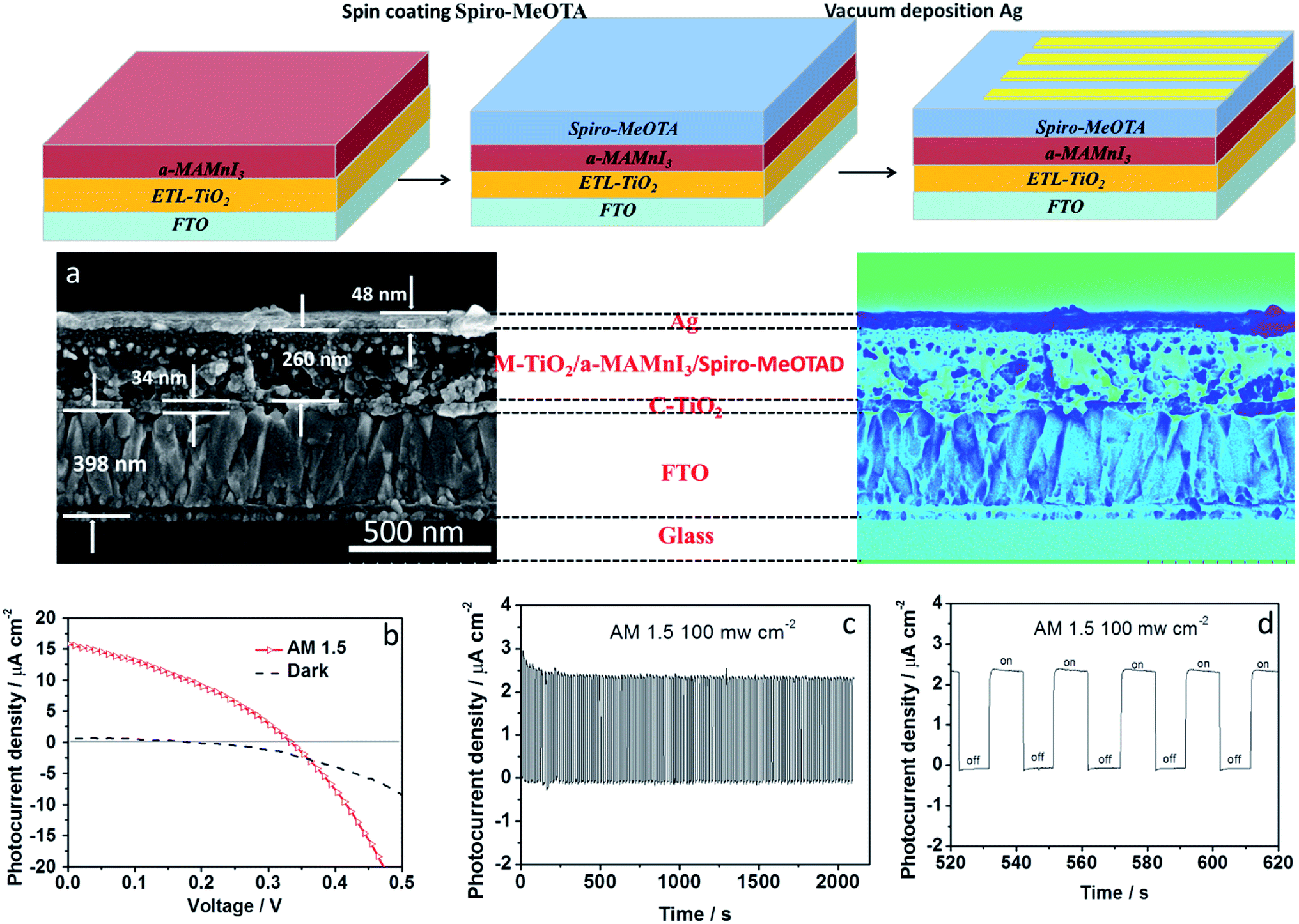 | ||
| Fig. 3 Schematic diagram of the solution-processed HTM and vacuum deposition Ag on FTO/ELT-TiO2/MAMnI3; (a) cross-sectional SEM images of FTO/ETL-TiO2/a-MAMnI3/Spiro-MeOTAD/Ag; (b) the photocurrent–voltage performance of the device were measured under AM1.5, 100 mW cm−2 simulated illumination; (c) photocurrent–time characteristics of the device under AM1.5, 100 mW cm−2 simulated illumination; (c) amplifying on/off signal in photocurrent-time characteristics. | ||
The photoelectric responses were investigated at different wavelengths to determine the monochromatic response of photocurrents. The different wavelengths of monochromatic light were obtained and depicted in Fig. 4. The chopping frequency of monochromatic light was 1.33 Hz. In our previous report, we found that the MA2MnCl4-based photoresponsive device exhibited ultraviolet photoresponse. However, the a-MAMnI3-based photoresponsive device presented obvious photoresponse not only to 300 nm ultraviolet light but also to 460 nm (blue) and 530 nm (green) visible light (Fig. 4). The large difference (Ion–Ioff) between the photocurrent intensity under illumination (Ion) and that in the dark (Ioff) is necessary in optoelectronic logic devices. The value of Ion–Ioff at 460 nm was greater than that at 300 and 530 nm. When the wavelength of monochromatic light was increased to 660 nm, the value of Ion–Ioff significantly decreased in Fig. S2 in ESI.† When the wavelength of the monochromatic light was increased to 760 and 860 nm, no photoelectric signal was observed, and the value of Ion–Ioff was close to zero in Fig. S2 in ESI.† The wavelength from 300 nm to 530 nm can be used as effective monochromatic light for a-MAMnI3 optoelectronic devices.
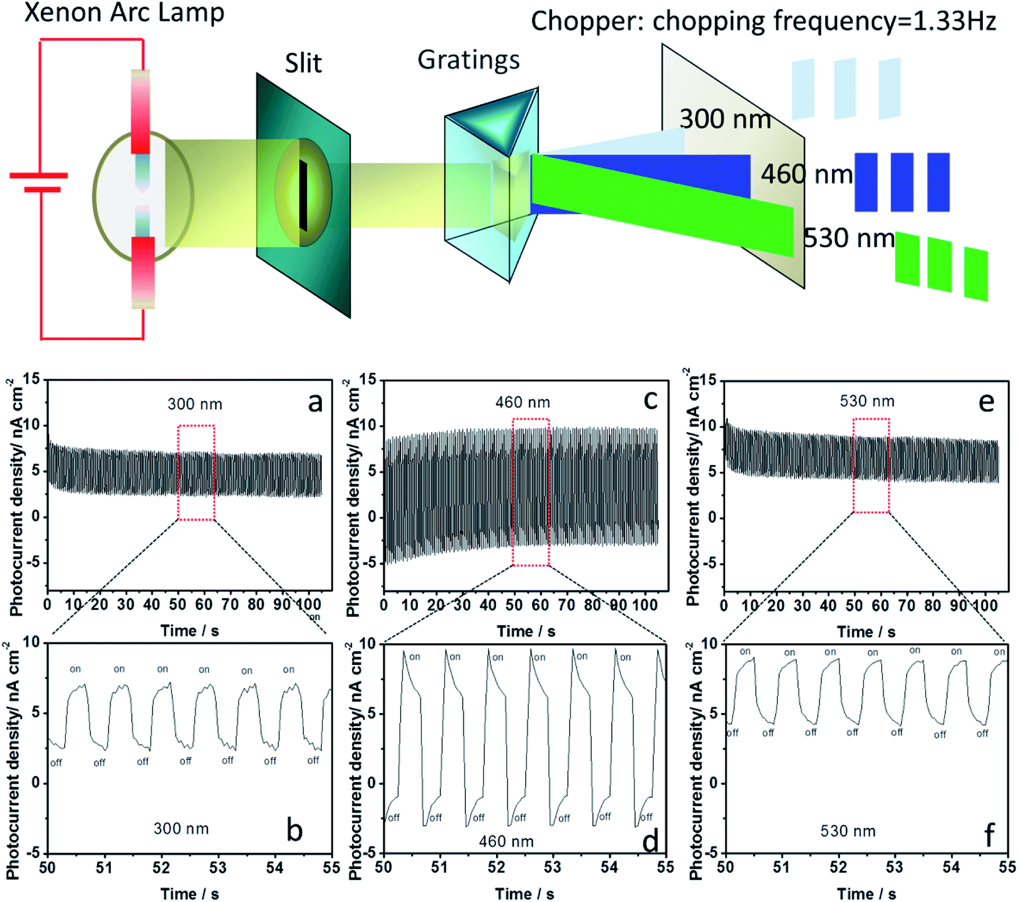 | ||
| Fig. 4 Schematic diagram of obtaining the different wavelengths of monochromatic light; photocurrent–time characteristics of the FTO/ETL-TiO2/a-MAMnI3/Spiro-MeOTAD/Ag device under different wavelengths (300, 460 and 530 nm) with 1.33 Hz chopping frequency. | ||
Conclusions
In sum, we prepared a Pb-free and amorphous MAMnI3 thin film via the spin coating method. Mesoscopic a-MAMnI3/TiO2 heterojunction was formed with the filling of a-MAMnI3 into the mesoporous TiO2 layer. The photovoltage of the optoelectronic device comprising FTO/ETL-TiO2/a-MAMnI3/Spiro-MeOTAD/Ag reached 300 mV under AM1.5, 100 mW cm−2 simulated illumination. Compared with MA2MnCl4 materials exhibiting ultraviolet photoresponse, the a-MAMnI3-based device presented obvious photoresponse not only to ultraviolet light but also to visible light (530 nm green). Finally, the test with 2000 s on/off cycling demonstrated the good stability and repeatability of the device. This Pb-free and amorphous organic–inorganic hybrid material will benefit the future industrial production of green and low-cost optoelectronic logic devices, photodetectors, and optical memory devices.Acknowledgements
This work was financially supported by Natural Science Foundation of Shandong Province (Grant No. ZR2016BQ20; BS2015NJ013; ZR2014BQ010; ZR2016BQ21), Colleges and universities in Shandong Province science and technology projects (Grant No. J16LC05; J17KA097), Science and Technology Innovation Foundation for the Uinversity or College Students (Grant No. 26312150518), Research Fund for the Doctoral Program of Liaocheng University (Grant No. 31805), National Natural Science Foundation of China (Grant No. 21503104; 21601078, 21171084), National Basic Research Program of China (Grant No. 2011CBA00701).Notes and references
- H. Xu, R. Chen, Q. Sun, W. Lai, Q. Su, W. Huang and X. Liu, Chem. Soc. Rev., 2014, 43, 3259–3302 RSC.
- M. de Pauli, U. Zschieschang, I. D. Barcelos, H. Klauk and A. Malachias, Adv. Electron. Mater., 2016, 2, 1500402 CrossRef.
- S. Mathew, A. Yella, P. Gao, R. Humphry-Baker, B. F. E. Curchod, N. Ashari-Astani, I. Tavernelli, U. Rothlisberger, M. K. Nazeeruddin and M. Graetzel, Nat. Chem., 2014, 6, 242–247 CrossRef CAS PubMed.
- T. Matsushima, F. Mathevet, B. Heinrich, S. Terakawa, T. Fujihara, C. J. Qin, A. S. D. Sandanayaka, J. C. Ribierre and C. Adachi, Appl. Phys. Lett., 2016, 109, 253301 CrossRef.
- X. L. Yang, G. J. Zhou and W. Y. Wong, Chem. Soc. Rev., 2015, 44, 8484–8575 RSC.
- K. Borjesson, P. Rudquist, V. Gray and K. Moth-Poulsen, Nat. Commun., 2016, 7(8), 12689 CrossRef CAS PubMed.
- A. Kojima, K. Teshima, Y. Shirai and T. Miyasaka, J. Am. Chem. Soc., 2009, 131, 6050–6051 CrossRef CAS PubMed.
- M. Saliba, T. Matsui, J. Y. Seo, K. Domanski, J. P. Correa-Baena, M. K. Nazeeruddin, S. M. Zakeeruddin, W. Tress, A. Abate, A. Hagfeldt and M. Gratzel, Energy Environ. Sci., 2016, 9, 1989–1997 CAS.
- G. Liu, L. P. Kong, J. Gong, W. G. Yang, H. K. Mao, Q. Y. Hu, Z. X. Liu, R. D. Schaller, D. Z. Zhang and T. Xu, Adv. Funct. Mater., 2017, 27, 1604208 CrossRef.
- G. E. Eperon, S. D. Stranks, C. Menelaou, M. B. Johnston, L. M. Herz and H. J. Snaith, Energy Environ. Sci., 2014, 7, 982–988 CAS.
- S. D. Stranks, G. E. Eperon, G. Grancini, C. Menelaou, M. J. P. Alcocer, T. Leijtens, L. M. Herz, A. Petrozza and H. J. Snaith, Science, 2013, 342, 341–344 CrossRef CAS PubMed.
- D. Kiermasch, P. Rieder, K. Tvingstedt, A. Baumann and V. Dyakonov, Sci. Rep., 2016, 6, 39333 CrossRef CAS PubMed.
- K. Galkowski, A. Mitioglu, A. Miyata, P. Plochocka, O. Portugall, G. E. Eperon, J. T. W. Wang, T. Stergiopoulos, S. D. Stranks, H. J. Snaith and R. J. Nicholas, Energy Environ. Sci., 2016, 9, 962–970 CAS.
- A. Miyata, A. Mitioglu, P. Plochocka, O. Portugall, J. T. W. Wang, S. D. Stranks, H. J. Snaith and R. J. Nicholas, Nat. Phys., 2015, 11, 582–594 CrossRef CAS.
- T. Nguyen Huy, Z. Ku and H. J. Fan, Adv. Energy Mater., 2016, 6, 1501420 CrossRef.
- T. A. Berhe, W.-N. Su, C.-H. Chen, C.-J. Pan, J.-H. Cheng, H.-M. Chen, M.-C. Tsai, L.-Y. Chen, A. A. Dubale and B.-J. Hwang, Energy Environ. Sci., 2016, 9, 323–356 CAS.
- H. Zhang, J. Cheng, F. Lin, H. He, J. Mao, K. S. Wong, A. K. Y. Jen and W. C. H. Choy, ACS Nano, 2016, 10, 1503–1511 CrossRef CAS PubMed.
- T. Zhang, H. N. Chen, Y. Bai, S. Xiao, L. Zhu, C. Hu, Q. Z. Xue and S. H. Yang, Nano Energy, 2016, 26, 620–630 CrossRef CAS.
- S. van Reenen, M. Kemerink and H. J. Snaith, J. Phys. Chem. Lett., 2015, 6, 3808–3814 CrossRef CAS PubMed.
- P. Umari, E. Mosconi and F. De Angelis, Sci. Rep., 2014, 4, 4467 CrossRef PubMed.
- L. Ma, F. Hao, C. C. Stoumpos, B. T. Phelan, M. R. Wasielewski and M. G. Kanatzidis, J. Am. Chem. Soc., 2016, 138, 14750–14755 CrossRef CAS PubMed.
- T. Krishnamoorthy, H. Ding, C. Yan, W. L. Leong, T. Baikie, Z. Zhang, M. Sherburne, S. Li, M. Asta, N. Mathews and S. G. Mhaisalkar, J. Mater. Chem. A, 2015, 3, 23829–23832 CAS.
- Z. H. Nie, J. Yin, H. W. Zhou, N. Chai, B. L. Chen, Y. T. Zhang, K. G. Qu, G. D. Shen, H. Y. Ma, Y. C. Li, J. S. Zhao and X. X. Zhang, ACS Appl. Mater. Interfaces, 2016, 8, 28187–28193 CAS.
- Y. Zhang, W.-Q. Liao, D.-W. Fu, H.-Y. Ye, Z.-N. Chen and R.-G. Xiong, J. Am. Chem. Soc., 2015, 137, 4928–4931 CrossRef CAS PubMed.
- P. Jain, V. Ramachandran, R. J. Clark, H. D. Zhou, B. H. Toby, N. S. Dalal, H. W. Kroto and A. K. Cheetham, J. Am. Chem. Soc., 2009, 131, 13626 CrossRef PubMed.
- Z. S. Bai, Z. P. Qi, Y. Lu, Q. Yuan and W. Y. Sun, Cryst. Growth Des., 2008, 8, 1924–1931 CAS.
- J. C. Tan, P. J. Saines, E. G. Bithell and A. K. Cheetham, ACS Nano, 2012, 6, 615–621 CrossRef CAS PubMed.
- L. Luo, Y. Zeng, L. Li, Z. Luo, T. I. Smirnova and P. A. Maggard, Inorg. Chem., 2015, 54, 7388–7401 CrossRef CAS PubMed.
- K. S. Asha, K. M. Ranjith, A. Yogi, R. Nath and S. Mandal, Dalton Trans., 2015, 44, 19812–19819 RSC.
- H. Zhou, Z. Nie, J. Yin, Y. Sun, H. Zhuo, D. Wang, D. Li, J. Dou, X. Zhang and T. Ma, RSC Adv., 2015, 5, 85344–85349 RSC.
- H. Zhou, Y. Shi, Q. Dong, H. Zhang, Y. Xing, K. Wang, Y. Du and T. Ma, J. Phys. Chem. Lett., 2014, 5, 3241–3246 CrossRef CAS PubMed.
- H. Zhou, Y. Shi, K. Wang, Q. Dong, X. Bai, Y. Xing, Y. Du and T. Ma, J. Phys. Chem. C, 2015, 119, 4600–4605 CAS.
Footnote |
| † Electronic supplementary information (ESI) available. See DOI: 10.1039/c7ra04235c |
| This journal is © The Royal Society of Chemistry 2017 |