
 Open Access Article
 This Open Access Article is licensed under a Creative Commons Attribution-Non Commercial 3.0 Unported Licence
Low-temperature solution-processed MoOx as hole injection layer for efficient quantum dot light-emitting diodes
Jingling Li abc,
Qiling Guoabd,
Hu Jinabc,
Kelai Wangabe,
Dehua Xuabc,
Gang Xuabc and
Xueqing Xu*abc
abc,
Qiling Guoabd,
Hu Jinabc,
Kelai Wangabe,
Dehua Xuabc,
Gang Xuabc and
Xueqing Xu*abc
aCAS Key Laboratory of Renewable Energy, Guangzhou Institute of Energy Conversion, Chinese Academy of Sciences, Guangzhou 510640, China. E-mail: xuxq@ms.giec.ac.cn
bGuangdong Provincial Key Laboratory of New and Renewable Energy Research and Development, Guangzhou 510640, China
cUniversity of Chinese Academy of Sciences, Beijing 100049, China
dSchool of Materials Science and Engineering, South China University of Technology, Guangzhou 510640, China
eSchool of Chemical Engineering and Light Industry, Guangdong University of Technology, Guangzhou 510006, China
First published on 23rd May 2017
Abstract
In this work, quantum dot light-emitting diodes (QD-LEDs) based on a low-temperature solution-processed MoOx hole injection layer were fabricated. As a result of the excellent wettability of the MoOx precursor, a smooth sMoOx HIL film with a roughness of less than 1 nm was obtained. In comparison with a device based on PEDOT:PSS, the best sMoOx-based QD-LED displayed comparable device performance in terms of a maximum luminance of 10![[thin space (1/6-em)]](https://www.rsc.org/images/entities/char_2009.gif) 225 cd m−2, a peak current efficiency of 4.04 cd A−1, a maximum external quantum efficiency of 1.61% and, more importantly, an approximately threefold increase in operational lifetime. Furthermore, we investigated the relationship between the thermal treatment of the sMoOx film and the device performance. UPS measurements revealed that the work function of the sMoOx film underwent an upshift from 5.51 to 4.90 eV when the annealing temperature was increased from 50 to 250 °C, which indicated that low-temperature treatment of the sMoOx HIL is beneficial for hole injection and EL performance. This demonstration of a bright, efficient and stable sMoOx-based QD-LED provides another feasible application of solution-processable transition metal oxide materials as the HIL within QD-LEDs and promotes the development of low-cost, all-solution-processed optoelectronic devices.
225 cd m−2, a peak current efficiency of 4.04 cd A−1, a maximum external quantum efficiency of 1.61% and, more importantly, an approximately threefold increase in operational lifetime. Furthermore, we investigated the relationship between the thermal treatment of the sMoOx film and the device performance. UPS measurements revealed that the work function of the sMoOx film underwent an upshift from 5.51 to 4.90 eV when the annealing temperature was increased from 50 to 250 °C, which indicated that low-temperature treatment of the sMoOx HIL is beneficial for hole injection and EL performance. This demonstration of a bright, efficient and stable sMoOx-based QD-LED provides another feasible application of solution-processable transition metal oxide materials as the HIL within QD-LEDs and promotes the development of low-cost, all-solution-processed optoelectronic devices.
1. Introduction
Colloidal semiconductor nanocrystals have attracted considerable attention in recent years owing to their desirable features such as size-tunable emission, narrow emission linewidth, high photoluminescence quantum yield and flexible solution-processability.1–3 One of the most groundbreaking products based on these outstanding materials is the so-called quantum dot light-emitting diode (QD-LED), which is a promising contender for the next generation of flat-panel displays and solid-state lighting.4–6 Ever since its first demonstration in 1994, substantial improvements have been made and the external quantum efficiency of this device has increased from less than 0.01% to over 20%.1,7,8 In spite of this significant progress, the design of efficient and stable QD-LEDs is still a challenge. The exploitation of appropriate electron and hole charge transport layers is paramount for coordinating the efficiency and stability of QD-LEDs. Among the various materials that are available for interfacial carrier transport layers, transition metal oxides (TMOs) have shown great potential owing to their wide range of possible energy level alignments.9 To date, electron transport materials such as zinc oxide (ZnO)10–12 and titanium dioxide (TiO2)13,14 have been widely used in QD-LEDs owing to their high electron mobility, energy levels that match those of semiconductor nanocrystals and facile film deposition by solution-processing. In spite of the outstanding electrical properties of QD-LEDs that use poly(3,4-ethylenedioxythiophene):poly(styrenesulfonate) (PEDOT:PSS), the high acidity and hygroscopicity of this polymer are usually associated with device instability. Therefore, the use of metal oxides of equivalent quality for hole conduction is still in demand as a replacement for PEDOT:PSS. Over a period of time, vacuum-deposited (e.g., by sputtering and thermal evaporation) metal oxides, including NiO, WO3, MoO3 and V2O5, have been extensively developed.15–20 However, this is generally not a cost-effective technique for meeting the requirements of industrial manufacture. Even though solution-processable WO3 NPs and NiO prepared via a sol–gel method have been successfully employed in QD-LEDs,21,22 their EL performance is still far from satisfactory.Recently, solution-processable non-stoichiometric MoOx (sMoOx) has stood out owing to its low-lying work function relative to that of an indium tin oxide (ITO, ∼4.8 eV) anode. For instance, Vu et al. demonstrated solution-processable MoOx with a work function of 5.6 eV, by which their sMoOx-based QD-LED exhibited an efficiency of 3.5%.23 However, this sMoOx film, which was formed from ammonium molybdate, requires a thermal decomposition process. Commercially available MoO3 nanoparticles (NPs) are another source used for obtaining a hole conduction layer. However, this MoO3 film requires oxygen plasma treatment to remove the polymer dispersant.24 Besides, a substantial drawback of using MoO3 NPs is the formation of large aggregates with a size of 100 nm and an overall large root-mean-square (RMS) roughness of the film of ∼25 nm, which obviously impairs device performance. Efficient deposition techniques via solution-processing for obtaining high-quality MoOx HILs are still in the early stages of development.
A facile synthetic route via the oxidation of Mo metal powder with the use of hydrogen peroxide has recently been reported by Xie et al., who confirmed that this sMoOx layer had the effect of enhancing hole extraction and prolonging the device operational lifetime of organic solar cells.9 In spite of these advantages, the application of QD-LEDs based on sMoOx prepared in this way has rarely been reported.
Therefore, in this work we employed MoOx prepared by a sol–gel method as the hole injection layer (HIL) for fabricating bright and efficient QD-LEDs. A sMoOx-based QD-LED exhibited a maximum luminance of 10225 cd m−2, a peak current efficiency of 4.04 cd A−1, a maximum external quantum efficiency of 1.61%, and, more importantly, an approximately threefold increase in operational lifetime, which indicated that our sMoOx-based device is competitive in comparison with the present PEDOT:PSS-based device. Furthermore, the device performance exhibited strong dependence on the thermal treatment of the sMoOx HIL. The temperature-dependent band structure of sMoOx was then studied by UPS measurements, which revealed that the low-lying work function of 5.51 eV underwent an upshift to 4.90 eV when the thermal treatment temperature was increased from 50 to 250 °C. This property led to differences in the hole transport behavior and EL performance of the QD-LED, which confirmed that low-temperature annealing is more beneficial for obtaining bright and efficient QD-LEDs.
2. Experimental
Synthesis of MoOx precursor
Firstly, 0.5 g molybdenum (Mo) powder was dispersed in 10 mL ethanol with vigorous stirring for 5 minutes. Then, 1 mL H2O2 (30%) was added to the molybdenum suspension. After reaction for 24 hours, the solution turned from grey to deep blue. This precursor solution was dried by vacuum distillation and redispersed in 10 mL ethanol.Synthesis of ZnCdSeS/ZnS QDs
The synthesis method was based on an established protocol with some modifications.25 Specifically, 1 mmol CdO (AR, 99%, Aladdin) and 8 mmol ZnO (AR, 99%, Aladdin) were mixed with 7 mL oleic acid (OA, AR, Aladdin) in a 50 mL three-necked flask. After being degasified and purged with nitrogen twice, the mixture was heated to 150 °C, during which vigorous stirring was continued. After the mixture had been held for 5 min at this temperature, 15 mL octadecene (ODE, >90.0%, Aladdin) was added to the mixture. Subsequently, the temperature was further increased to 300 °C. An anionic stock solution, which was prepared separately by dissolving 2 mmol sulfur (S) powder and 0.4 mmol selenium (Se) powder in 2 mL tributylphosphine (TBP, 95%, Aladdin), was rapidly injected into the above hot mixture. The reaction was maintained at that temperature for 10 min to enable the growth of QDs with a ZnCdSeS core. For the subsequent coating with a ZnS shell, a second stock solution of S containing 4 mmol S dissolved in 5 mL OA was injected dropwise at a rate of ∼0.5 mL min−1, and the shell formation reaction was continued for 3 h. The colloidal NCs that were obtained were precipitated by the addition of excess ethanol and subsequent centrifugation at 8000 rpm for 5 min and were dispersed in n-hexane after the supernatant was decanted. This purification process was repeated five times under the same conditions. Finally, the purified QDs were redispersed in n-octane for spin-coating with the EML.Synthesis of ZnO nanoparticles
The ZnO NPs used in this work were synthesized using a method proposed in the literature.26 A solution of the cation was prepared by dissolving 3 mmol zinc acetate hydrate in 30 mL dimethyl sulfoxide. Subsequently, another solution, which was prepared by dissolving 5 mmol tetramethylammonium hydroxide in 10 mL ethanol, was slowly added to the above solution of the cation within 1 minute. This reaction proceeded at room temperature for 1 hour. Finally, the ZnO NPs were washed via a multi-step process comprising precipitation (using ethyl acetate) and redispersion (using ethanol).Device fabrication
Patterned ITO glass substrates were sequentially cleaned with methanol, acetone, ethanol, and finally deionized water. Then, the dried ITO substrates were processed by ultraviolet ozone (UVO) treatment for 15 minutes. After the above procedures, an sMoOx layer was spin-coated at 4000 rpm onto ITO for 40 s and then annealed at a different temperature for 10 min. A solution (5 mg mL−1), which was prepared by dissolving poly(9-vinylcarbazole) (PVK) (Aldrich, average MW = 120000) in chlorobenzene, was deposited on top of sMoOx for 40 s to form the hole transport layer (HTL), followed by baking at 150 °C for 20 min. The emitting layer (EML) was spin-deposited using ZnCdSeS/ZnS QDs dispersed in n-octane with a concentration of 20 mg mL−1 at 3000 rpm for 40 s, followed by baking at 70 °C. A transparent ethanolic solution of ZnO NPs with a concentration of 20 mg mL−1 was then spin-coated at 2000 rpm for 40 s, followed by baking at 70 °C for 30 min to produce a compact ZnO layer. Next, vacuum deposition of a silver (Ag) cathode with a thickness of 120 nm on top of the ZnO ETL was carried out to complete the entire structure of the QD-LED. All layers except the Ag cathode were deposited under ambient conditions.
Characterization
The contact angle between ITO and the HIL solutions was measured by a contact angle measuring instrument (JD-901A), and the surface morphologies of the deposited layers were studied by atomic force microscopy (AFM, Bruker Multimode 8). A field emission scanning electron microscope (SEM) (Hitachi S-4800) operated at 10 kV was used to measure the thickness of the individual layers in multi-layer QD-LEDs. High-resolution transmission electron microscopy (HRTEM) images were obtained using a JEM-2100F TEM operated at an accelerating voltage of 200 kV. Ultraviolet photoelectron spectroscopy (Escalab 250Xi) was used to investigate the band structure of the sMoOx film. Photoluminescence (PL) spectra were recorded with a Lambda LS55 spectrophotometer, and absorption spectra were recorded with a PerkinElmer Lambda 750 UV/vis/NIR spectrophotometer. The electroluminescence (EL) spectrum of the QD-LED was recorded using an Ocean USB 2000+ fiber optic spectrometer. The current density–voltage–luminance (J–V–L) characteristics of QD-LEDs were measured with a Keithley 2420 source meter and a silicon photodiode calibrated by a PR655 spectroradiometer under ambient conditions.3. Results and discussion
To replace a PEDOT:PSS layer with an sMoOx layer in a QD-LED, a desirable criterion for the employment of solution-processed modifying layers is that their surface structure should be as smooth as possible. This is because a smooth film surface is usually a favorable precondition for preventing a large leakage current through the device and to achieve homogeneous charge transfer through the interfacial layers.23 In this respect, excellent wetting properties between the solution employed and the sub-layer are usually required to form high-quality spin-coated layers. Fig. 1 depicts the contact angles of an aqueous solution of PEDOT:PSS and an alcoholic solution of MoOx on ITO-coated glass substrates, which had been adequately cleaned and some of which had been subjected to UVO treatment. With non-UVO-treated ITO as a contact surface, a droplet of the PEDOT:PSS solution that spread on ITO had a relatively large contact angle of 28.16°, as shown in Fig. 1a. This indicates poor wettability between PEDOT:PSS and non-UVO-treated ITO. Even though the contact angle decreased to 18.28° when the ITO substrate had been processed by UVO treatment (see Fig. 1b), we found that the alcoholic solution of MoOx displayed better wettability performance on the ITO substrates. Fig. 1c shows a smaller contact angle of 16.53° when an sMoOx droplet spread on the UVO-treated ITO substrate. Moreover, the wetting properties between sMoOx and ITO were further improved when the ITO substrate had been processed by UVO treatment. Fig. 1d shows the process of contact between MoOx and UV-ozone-treated ITO. An obvious feature during this process is that the MoOx droplet swiftly spread out onto the ITO substrate, which indicated the superior wettability of the alcoholic solution of MoOx. | ||
| Fig. 1 Contact angles of solutions of PEDOT:PSS and sMoOx on ITO-coated glass substrates: (a) PEDOT:PSS on untreated ITO; (b) PEDOT:PSS on UV-ozone-treated ITO; (c) sMoOx on untreated ITO; (d) sMoOx on UV-ozone-treated ITO. Inset in lower left of the (d) image shows the sMoOx droplet before contact and that in the upper right displays a complete wetting for sMoOx solution on ITO substrate. | ||
The resulting surface topologies revealed by AFM images are presented in Fig. 2. The measured values of surface RMS roughness for PEDOT:PSS films on non-UVO-treated and UVO-treated ITO substrates (which correspond to Fig. 2a and b) were 1.45 nm and 1.03 nm, respectively. The line scan profiles in Fig. 2c reveal that the wetting properties of PEDOT:PSS were greatly affected by the UVO treatment. In contrast, the sMoOx films exhibited similar wetting properties on both ITO substrates regardless of whether the ITO substrate had been processed by UVO treatment. Each sMoOx film displayed a remarkably similar surface structure, with RMS roughness values ranging between ∼0.8 and 1.0 nm (Fig. 2d and e) and peak-to-trough values of ∼2 nm (Fig. 2f). The deposition of sMoOx onto ITO was found to result in the formation of a more homogeneous film. In general, all these RMS values of sMoOx films are sufficiently smooth for incorporation into a QD-LED. The good wettability of sMoOx on ITO resulted in this smooth surface. PEDOT:PSS was also found to form a homogeneous coating on the ITO surface; however, it did so via the formation of nanoparticle films.27 This factor caused the comparative surface roughness to increase slightly to above 1 nm.
 | ||
| Fig. 2 AFM topological images of PEDOT:PSS films on (a) non-UVO-treated and (b) UVO-treated substrates. (c) The corresponding line scan profiles for the PEDOT:PSS films. AFM images of sMoOx films on (d) non-UVO-treated and (e) UVO-treated substrates. (f) Selected line scan profiles for the sMoOx films. | ||
Device performance
As illustrated in Fig. 3a, a typical QD-LED fabricated in this work consisted of a multi-layered structure of an ITO anode, layers of sMoOx (∼18 nm), PVK (∼8 nm), ZnCdSeS/ZnS QDs (∼35 nm), and ZnO NPs (∼40 nm) and an Ag (120 nm) cathode. Fig. 3b shows a schematic of the flat-band energy level diagram for this multi-layered QD-LED. The sizes of the thick-shell QDs and ZnO NPs were estimated to be ∼10 nm and ∼4 nm, respectively, as can be seen from the TEM images in Fig. 3c and d. The PL quantum yield of the QDs that were employed was ∼83%. The film thickness of the individual sMoOx layer was measured from a cross-sectional SEM image (∼18 nm, see Fig. 3e). It should be noted that the employment of a PVK layer is essential in current device architectures. This is because, on the one hand, ethanol in the ZnO solution can permeate through the QDs layer and thereby cause damage to the existing sMoOx layer if it lacks the protection of a compact PVK layer. On the other hand, the suitable HOMO (∼5.8 eV) and LUMO (∼2.2 eV) energy levels of the PVK layer make it possess the dual functions of hole transporting and electron blocking in QD-LEDs.1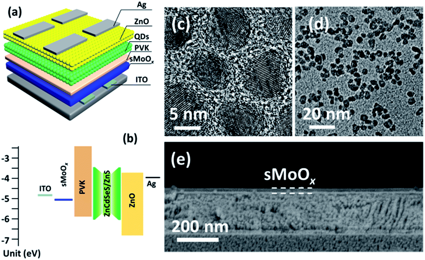 | ||
| Fig. 3 (a) Device architecture of QD-LED using sMoOx to replace PEDOT:PSS. (b) Flat-band diagram for the multi-layered QD-LED. TEM images of (c) thick-shell ZnCdSeS/ZnS QDs and (d) ZnO NPs. (e) Cross-sectional SEM image of the smooth, uniform sMoOx layer on the ITO substrate. | ||
Fig. 4 compares the EL characteristics of sMoOx-based and PEDOT:PSS-based QD-LEDs in terms of luminance (L), current efficiency (CE) and external quantum efficiency (EQE). Both devices were fabricated by the same solution process, and PEDOT:PSS layers of similar thicknesses (∼20 nm at 6000 rpm) were employed. In Fig. 4a, even though the PEDOT:PSS-based QD-LED exhibited a lower turn-on voltage (defined as L > 1 cd m−2) of 3.1 eV and a larger maximum L value of 10267 cd m−2 (at 5.2 V), its sMoOx-based counterpart displayed a broader range of operating voltages from the turn-on voltage of 4.8 V to 10 V. In other words, efficiency roll-off easily occurred for the PEDOT:PSS-based device when the applied voltage exceeded 5.2 V (which corresponds to a J value of ∼100 mA cm−2), whereas the sMoOx-based device remained stable in normal working conditions. This operational stability is particularly important in practical applications. In fact, the maximum L value of the sMoOx-based QD-LED reached 10225 cd m−2, which is comparable to that of the PEDOT:PSS-based device in this study or in some other works.28,29 Fig. 4b and c show the dependences of the values of L and CE/EQE on the J value. Two distinct advantages of the sMoOx-based device in comparison with the PEDOT:PSS-based device can be found. On one hand, when the QD-LED is operated in working conditions with a low J value (<25 mA cm−2), the performance parameters in terms of the values of L, CE and EQE achieved by the sMoOx-based device were more advantageous. On the other hand, the sMoOx-based device exhibited a wider operating window in terms of J values (0–600 mA cm−2). The degradation of the PEDOT:PSS-based device at J values in excess of 100 mA cm−2 could possibly be ascribed to luminance quenching due to a carrier imbalance in the QD layer.1,15,30 Fig. 4d shows the dependence of EQE on luminance. The highest EQE values for both devices were achieved at a relatively high luminance (>4000 cd m−2). More importantly, we should note that the sMoOx-based device exhibited a higher EQE at luminances of less than 674 cd m−2, which is more desirable in display applications.
 | ||
| Fig. 4 (a) J–V, (b) L–J, (c) CE–J–EQE and (d) EQE–L relations for sMoOx-based and PEDOT:PSS-based devices. | ||
The variations in relative luminance versus time for unencapsulated green QD-LEDs operated at a constant current density of 20 mA cm−2 under atmospheric conditions are shown in Fig. 5. The initial luminances (L0) for the sMoOx- and PEDOT:PSS-based devices were ∼760 cd m−2 and ∼650 cd m−2, respectively. Interestingly, we found that the L values for both devices increased slightly for several minutes only, after which the values of L/L0 decreased monotonically, as shown in Fig. 5. This case is very similar to one reported in the literature10 and may be caused by gradual illumination from the electrode edge to the entire emitting region. The half-life (T50), which is defined as the time taken for the luminance to decrease to L0/2,1 for the sMoOx-based QD-LED was 1.36 h, which was longer than that for the PEDOT:PSS-based device (0.52 h). Therefore, the employment of sMoOx as the EIL is more beneficial for maintaining device performance during long-term operation.
 | ||
| Fig. 5 Operational lifetime characteristics of the resulting sMoOx-based and optimized PEDOT:PSS-based QD-LEDs without encapsulation. The devices were operated continuously at a constant current density (20 mA cm−2). | ||
Effects of thermal treatment
Thermal treatment of the spin-coated layer is usually required in the fabrication of QD-LEDs, not only for removing organic solvents but also for improving the interfacial contact of the transport layers. Fig. 6a presents the J–V curves of QD-LEDs as a function of the annealing temperature. Two obvious tendencies can be found. Firstly, the turn-on voltage gradually increased from 4.8 V to 5.5 V when the sMoOx layer was subjected to a higher annealing temperature. This may suggest that the barrier to hole injection became higher within this ITO/sMoOx/PVK structure when sMoOx was annealed at a higher temperature. On the other hand, the maximum luminance decreased from 10225 cd m−2 to 5684 cd m−2, which shows that the device performance was directly influenced by thermal treatment. Fig. 6b and c show the luminance, current efficiency and external quantum efficiency as a function of the current density. They show that the QD-LED with an sMoOx HIL treated at low temperature exhibited the best performance in the range of 0–500 mA cm−2. The highest CE and EQE values for the sMoOx-based QD-LED treated at 50 °C were 4.04 cd A−1 and 1.61%, respectively, whereas those for the device annealed at 250 °C dramatically decreased to 1.65 cd A−1 and 0.66%, respectively, which indicated that high-temperature annealing of the sMoOx layer was unconducive to improving or even retaining the device performance. The same conclusion can be reached when the devices were operated in conditions of constant luminance, as can be seen in Fig. 6d.
 | ||
| Fig. 6 Characteristics of QD-LEDs with different sMoOx HILs annealed at 50 °C, 150 °C and 250 °C, respectively. (a) J–V–L relations; (b) L versus J; (c) CE versus J; (d) EQE versus L. | ||
To investigate the temperature-dependent mechanism behind this change in device performance, the electronic structure of the sMoOx film was studied via UPS measurements. From the UPS spectra shown in Fig. 7a, a work function (φ) was determined according to the formula φ = 21.22 + Ecut-off − EFermi, where Ecut-off and EFermi represent the kinetic energies at the secondary-electron cutoff and the Fermi edge, respectively. The valence band maximum (VBM) was estimated by the equation EVB = φ + |ΔE|, where ΔE is the kinetic energy offset from the VB margin to the Fermi edge. Fig. 7b shows the (Ahv)2–hv relations for different sMoOx films, by which the width of the optical band gap and the position of the conduction band minimum (CBM) were determined. The band structures for the different sMoOx films are outlined in Fig. 7c, which reveals that the φ value underwent an upshift from 5.51 to 4.90 eV when sMoOx was subjected to a higher temperature, which is very similar to the case reported by Heeger et al.27 A corresponding upshift in the CBM from 5.33 to 4.85 eV also occurred. Such variations in the band structure of sMoOx led to differences in hole injection behavior in QD-LEDs. Fig. 8a shows the J–V relations for hole-only devices based on sMoOx with different annealing treatments with an architecture of ITO/sMoOx (various annealing treatments)/PVK/QD/sMoOx (50 °C)/Ag. Fitting was carried out to distinguish the transition in the mode of current conduction. It can be seen that the transition voltage from the ohmic type (where J ∝ V) to the space-charge-limited/trap-limited types31 (where J ∝ Vn) gradually increased in accordance with the change in the turn-on voltage in the corresponding sMoOx-based devices. These J–V relations confirm that an increase in the injection barrier at the sMoOx/PVK interface occurred when the CBM of sMoOx changed from 5.33 to 4.85 eV, as illustrated in Fig. 8b.
 | ||
| Fig. 7 (a) UPS spectra of sMoOx films after different thermal treatments. (b) Plot of (Ahν)2 versus photon energy for the determination of the optical energy band gap. (c) Band diagram of different sMoOx films. | ||
 | ||
| Fig. 8 (a) J–V characteristics for hole-only devices with a structure of ITO/sMoOx/PVK/QD/sMoOx/Ag. (b) Hole injection behavior of HIL/HTL structure when the sMoOx HIL was annealed at different temperatures. | ||
Here, the performance of devices with various kinds of HIL was compared, as summarized in Table 1. Even though the PEDOT:PSS-based device exhibited better performance in terms of maximum values of L, CE and EQE, the higher EQE of its sMoOx-based counterpart in conditions of low luminance, as well as its longer operational lifetime, as discussed above, are more competitive for practical applications. Furthermore, the performance of a WO3-based QD-LED, as demonstrated by Sun et al.,21 is also presented in Table 1. In comparison with this WO3-based QD-LED, the most remarkable advantage of our sMoOx-based QD-LEDs is their higher EQE value, which shows that sMoOx has similar properties to WO3 in achieving high performance of QD-LEDs.
| Device | Maximum luminance (cd m−2) | Driving voltage (V) | Current efficiency (cd A−1) | Maximum EQE (%) | |||
|---|---|---|---|---|---|---|---|
| Turn-on | @1000 cd m−2 | Maximum | @1000 cd m−2 | ||||
| PEDOT:PSS-based | 10267 |
3.1 | 5.2 | 10.35 | 3.99 | 4.14 | |
| sMoOx-based | 50 °C | 10225 |
4.8 | 8.2 | 4.04 | 3.68 | 1.61 |
| 150 °C | 7949 | 5.2 | 8.7 | 3.51 | 3.30 | 1.40 | |
| 250 °C | 5684 | 5.6 | 8.8 | 1.65 | 1.32 | 0.66 | |
| WO3-based21 | 21300 |
3.0 | N/A | 4.4 | N/A | 1.30 | |
Fig. 9a compares the EL spectrum of the sMoOx-based device with the PL emission of QDs. No spectral broadening was found but a red shift of ∼7 nm was observed for this sMoOx-based device. This red shift is attributed to the combined effect of an enhancement in inter-dot interactions that arose as a result of the reduced distances in the close-packed ZnCdSeS/ZnS film, an electric-field-induced Stark effect and long-range resonance transfer of electronic excitations from small to large dots.32–34 The symmetric emission peak centered at 518 nm with a full width at half maximum (FWHM) value of 44 nm corresponds to the Commission Internationale de l’Eclairage (CIE) coordinate at (0.15, 0.65), which represents a color-saturated deep green emission ideal for display applications (Fig. 9b).
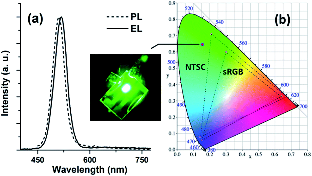 | ||
| Fig. 9 (a) Comparison of PL emission versus EL spectrum. The inset is an EL image of the sMoOx-based QD-LED. (b) Commission Internationale de l’Eclairage (CIE) coordinate for the EL emission. | ||
4. Conclusions
In summary, we have demonstrated a bright, efficient QD-LED with the employment of MoOx prepared by a sol–gel method and solution-processed at low temperatures as the hole injection layer. By the use of solution processing to deposit an anode modified layer, we found that sMoOx possessed better wettability relative to an aqueous solution of PEDOT:PSS, i.e., a smaller contact angle with the ITO layer, which led to a smooth HIL surface with an RMS value of less than 1 nm. Besides, we investigated the effect of annealing treatment on device performance. We found that low-temperature treatment of sMoOx was more favorable for achieving high performance of QD-LEDs. This was because the work function of the sMoOx film underwent an upshift from 5.51 to 4.90 eV when the annealing temperature was increased from 50 °C to 250 °C, which led to an increase in the barrier to hole injection at the sMoOx/PVK interface. Our optimized sMoOx-based QD-LED exhibited a maximum L value of 10225 cd m−2, a peak CE of 4.04 cd A−1 and a maximum EQE of 1.61%. Besides, the device lifetime was remarkably increased in comparison with that of a PEDOT:PSS-based QD-LED, which marks a further step towards the practical application of QD-LED technology. We judge that the overall performance of the sMoOx-based QD-LED has become competitive with respect to that of a current PEDOT:PSS-based QD-LED with the same device architecture. This work provides another feasible application of solution-processed TMO materials as HILs in QD-LEDs, which holds great promise in low-cost, all-solution-processed QD-LEDs and possibly has important implications for the development of all-inorganic-structure light-emitting devices.
Acknowledgements
This work was supported by the National Natural Science Foundation of China (projects 21273241), the Natural Science Foundation of Guangdong Province (2015A030310501), the Project on the Collaborative Innovation and Environmental Construction Platform of Guangdong Province (2014A050503051), and the Key Project on Synergy Collaborative Innovation of Guangzhou City (201704030069).References
- X. Dai, Z. Zhang, Y. Jin, Y. Niu, H. Cao, X. Liang, L. Chen, J. Wang and X. Peng, Nature, 2014, 515, 96–99 CrossRef CAS PubMed.
- J. Kwak, W. K. Bae, D. Lee, I. Park, J. Lim, M. Park, H. Cho, H. Woo, D. Y. Yoon, K. Char, S. Lee and C. Lee, Nano Lett., 2012, 12, 2362–2366 CrossRef CAS PubMed.
- Y. Zhang, C. A. Xie, H. P. Su, J. Liu, S. Pickering, Y. Q. Wang, W. W. Yu, J. K. Wang, Y. D. Wang, J. I. Hahm, N. Dellas, S. E. Mohney and J. A. Xu, Nano Lett., 2011, 11, 329–332 CrossRef CAS PubMed.
- K. H. Lee, C. Y. Han, H. D. Kang, H. Ko, C. Lee, J. Lee, N. Myoung, S. Y. Yim and H. Yang, ACS Nano, 2015, 9, 10941–10949 CrossRef CAS PubMed.
- W. K. Bae, J. Kwak, J. Lim, D. Lee, M. K. Nam, K. Char, C. Lee and S. Lee, Nano Lett., 2010, 10, 2368–2373 CrossRef CAS PubMed.
- J. L. Li, H. Jin, K. L. Wang, D. H. Xie, D. H. Xu, X. Q. Xu and G. Xu, RSC Adv., 2016, 6, 72462–72470 RSC.
- V. L. Colvin, M. C. Schlamp and A. P. Alivisatos, Nature, 1994, 370, 354–357 CrossRef CAS.
- B. S. Mashford, M. Stevenson, Z. Popovic, C. Hamilton, Z. Q. Zhou, C. Breen, J. Steckel, V. Bulovic, M. Bawendi, S. Coe-Sullivan and P. T. Kazlas, Nat. Photonics, 2013, 7, 407–412 CrossRef CAS.
- F. Xie, W. C. Choy, C. Wang, X. Li, S. Zhang and J. Hou, Adv. Mater., 2013, 25, 2051–2055 CrossRef CAS PubMed.
- L. Qian, Y. Zheng, J. G. Xue and P. H. Holloway, Nat. Photonics, 2011, 5, 543–548 CrossRef CAS.
- K. H. Lee, C. Y. Han, H. D. Kang, H. Ko, C. Lee, J. Lee, N. Myoung, S. Y. Yim and H. Yang, ACS Nano, 2015, 9, 10941–10949 CrossRef CAS PubMed.
- H. Zhang, H. Li, X. Sun and S. Chen, ACS Appl. Mater. Interfaces, 2016, 8, 5493–5498 CAS.
- T. H. Kim, K. S. Cho, E. K. Lee, S. J. Lee, J. Chae, J. W. Kim, D. H. Kim, J. Y. Kwon, G. Amaratunga, S. Y. Lee, B. L. Choi, Y. Kuk, J. M. Kim and K. Kim, Nat. Photonics, 2011, 5, 176–182 CrossRef CAS.
- K. S. Cho, E. K. Lee, W. J. Joo, E. Jang, T. H. Kim, S. J. Lee, S. J. Kwon, J. Y. Han, B. K. Kim, B. L. Choi and J. M. Kim, Nat. Photonics, 2009, 3, 341–345 CrossRef CAS.
- J. M. Caruge, J. E. Halpert, V. Wood, V. Bulovic and M. G. Bawendi, Nat. Photonics, 2008, 2, 247–250 CrossRef CAS.
- V. Wood, M. J. Panzer, J. M. Caruge, J. E. Halpert, M. G. Bawendi and V. Bulovic, Nano Lett., 2010, 10, 24–29 CrossRef CAS PubMed.
- V. Wood, M. J. Panzer, J. E. Halpert, J. M. Caruge, M. G. Bawendi and V. Bulovic, ACS Nano, 2009, 3, 3581–3586 CrossRef CAS PubMed.
- K. Hong, K. Kim, S. Kim, I. Lee, H. Cho, S. Yoo, H. W. Choi, N.-Y. Lee, Y.-H. Tak and J.-L. Lee, J. Phys. Chem. C, 2011, 115, 3453–3459 CAS.
- H. Kanno, R. J. Holmes, Y. Sun, S. Kena-Cohen and S. R. Forrest, Adv. Mater., 2006, 18, 339–342 CrossRef CAS.
- J. Wu, J. Hou, Y. Cheng, Z. Xie and L. Wang, Semicond. Sci. Technol., 2007, 22, 824–826 CrossRef CAS.
- X. Yang, Y. Ma, E. Mutlugun, Y. Zhao, K. S. Leck, S. T. Tan, H. V. Demir, Q. Zhang, H. Du and X. W. Sun, ACS Appl. Mater. Interfaces, 2014, 6, 495–499 CAS.
- N. Huu Tuan, N. Nang Dinh and S. Lee, Nanotechnology, 2013, 24, 115201 CrossRef PubMed.
- H.-T. Vu, Y.-K. Su, R.-K. Chiang, C.-Y. Huang, C.-J. Chen and H.-C. Yu, IEEE Photonics Technol. Lett., 2016, 28, 2156–2159 CrossRef.
- J. Meyer, R. Khalandovsky, P. Gorrn and A. Kahn, Adv. Mater., 2011, 23, 70–73 CrossRef CAS PubMed.
- K. H. Lee, J. H. Lee, H. D. Kang, B. Park, Y. Kwon, H. Ko, C. Lee, J. Lee and H. Yang, ACS Nano, 2014, 8, 4893–4901 CrossRef CAS PubMed.
- K. H. Lee, J. H. Lee, W. S. Song, H. Ko, C. Lee, J. H. Lee and H. Yang, ACS Nano, 2013, 7, 7295–7302 CrossRef CAS PubMed.
- J. J. Jasieniak, J. Seifter, J. Jo, T. Mates and A. J. Heeger, Adv. Funct. Mater., 2012, 22, 2594–2605 CrossRef CAS.
- H. Zhang, H. Li, X. Sun and S. Chen, ACS Appl. Mater. Interfaces, 2016, 8, 5493–5498 CAS.
- C. Jiang, H. Liu, B. Liu, Z. Zhong, J. Zou, J. Wang, L. Wang, J. Peng and Y. Cao, Org. Electron., 2016, 31, 82–89 CrossRef CAS.
- V. I. Klimov, A. A. Mikhailovsky, D. W. McBranch, C. A. Leatherdale and M. G. Bawendi, Science, 2000, 287, 1011–1013 CrossRef CAS PubMed.
- P. E. Burrows, Z. Shen, V. Bulovic, D. M. McCarty, S. R. Forrest, J. A. Cronin and M. E. Thompson, J. Appl. Phys., 1996, 79, 7991–8006 CrossRef CAS.
- J. M. Caruge, J. E. Halpert, V. Bulovic and M. G. Bawendi, Nano Lett., 2006, 6, 2991–2994 CrossRef CAS PubMed.
- C. R. Kagan, C. B. Murray and M. G. Bawendi, Phys. Rev. B: Condens. Matter Mater. Phys., 1996, 54, 8633–8643 CrossRef CAS.
- L. F. Sun, J. J. Choi, D. Stachnik, A. C. Bartnik, B. R. Hyun, G. G. Malliaras, T. Hanrath and F. W. Wise, Nat. Nanotechnol., 2012, 7, 369–373 CrossRef CAS PubMed.
| This journal is © The Royal Society of Chemistry 2017 |