
 Open Access Article
 This Open Access Article is licensed under a
 Creative Commons Attribution 3.0 Unported Licence
Negative differential resistance and spin filter effects in VS2 monolayers
G. W. Peng ,
L. Zhu and
K. L. Yao*
,
L. Zhu and
K. L. Yao*
School of Physics, Wuhan National High Magnetic Field Center, Huazhong University of Science and Technology, Wuhan 430074, China. E-mail: klyao@mail.hust.edu.cn
First published on 5th July 2017
Abstract
To determine the transport properties of VS2 monolayers, we have calculated the current based on the bias voltage, band structure and transmission spectrum for VS2 monolayers along the zigzag and armchair orientations by first-principles calculations combined with the non-equilibrium Green's function method. A perfect spin filtering effect for the two directions and strong anisotropy have been found. Meanwhile, the zigzag orientation device shows obvious negative differential resistance around a bias voltage of ±0.55 V.
1. Introduction
Due to the unique electronic structure and potential applications of graphene,1–4 atomically thin layered materials have received much attention as substitutes for silicon-based semiconductor materials in nanoscale electronics.5–8 Theory and experiments have proved the stability and unique electronic structure of a series of layered materials, such as silicene, germanene, stanene, phosphorene and transition-metal dichalcogenides (TMDs).9–15 Among these materials, TMDs show advantages in semiconducting devices because their layer structure means that atomically thin films can be easily obtained with various physical properties, including semiconductor properties, ferromagnetism, superconductor properties and so on.16–20So far, magnetism has not been found in most of the pristine graphene-like transition-metal dichalcogenides, and to obtain magnetism, the materials need an external electric field, a substrate, vacancies and strain, or should be doped with metal ions, which is not easy to control in an experiment. Recently, some research has found that half-metallicity, which can be applied in spintronic devices with high spin-polarized materials, can exist in pure layered TMDs including VS2 and VSe2 according to first-principles calculations.21–24 Compared to other half-metallic compounds, such as transition-metal pnictides and chalcogenides (TM-PCs) with zinc-blende (ZB) structures and Heusler's alloys, where the stability of the half-metallic property depends on the thickness and arrangement of surface atoms,25–27 these TMDs can retain half-metallicity without considering the state of the surface. Hence, TMD half-metals are more suitable for application in integrated circuits as spintronics.
Previous research has shown the existence of strong anisotropy of transport in some layered TMD insulators, such as MoS2 and MoSe2, in which the resistance of the device with the armchair orientation is larger than that of the device with the zigzag orientation.28 Due to it having the same structure, this may also occur in layered VS2. To demonstrate the transport properties for spintronic applications, here we theoretically designed two kinds of devices based on VS2 monolayers. The results show that the spin filtering effect is obtained in both devices, and negative differential resistance (NDR) exists in the VS2 monolayer with the zigzag orientation, which makes the VS2 monolayer a promising candidate for spintronics.
2. Computational methods
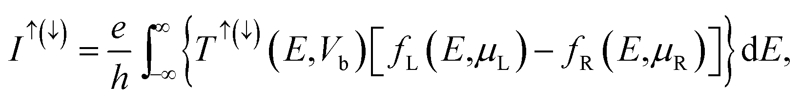
We established two kinds of hexagonal monolayer VS2 devices which are placed along the z-direction with zigzag and armchair orientations, respectively. Based on first-principles calculations combined with the non-equilibrium Green's function method (ATK code),29–31 we have calculated the spin transport properties. The Perdew–Burke–Ernzerhof (PBE) generalized gradient approximation (GGA) was used for the exchange–correlation potential.32 In the calculation, we used k sampling of 1 × 1 × 100 and a real space grid of 180 Ry for the current, and the electron temperature in the Fermi function was 300 K. A 15 nm vacuum along the Z axis was applied to avoid interactions between the layers. The spin-dependent charge current through the device was calculated using the Landauer–Büttiker formula:where T↑(↓)(E) is the spin-dependent transmission function defined by T↑(↓)(E,Vb) = Tr[TLGRTRGL]↑(↓), fL(R)(E) is the Fermi distribution function of electrons in the left (right) electrodes, and μL(R) = EF ± eVb/2 is the chemical potential of the left and right electrodes.
3. Results and discussion
The devices based on VS2 monolayers in the zigzag orientation and armchair orientation are shown in Fig. 1. The spin-resolved currents as a function of bias voltage (I–V characteristics) from −1 to 1 V for both directions are shown in Fig. 2. For the device in the zigzag orientation, the spin-up current rises immediately and increases rapidly with a small bias, and becomes gentle when the bias is raised to 0.2 V. Once the bias exceeds 0.4 V, a significant NDR behavior appears, where the current reduces as the bias increases, and then increases approximately linearly after 0.55 V of bias. Meanwhile, the spin-down current is neglected within the whole bias voltage range. For the armchair orientation device, the spin-down current is almost zero, while the spin-up one arises after the voltage rises to 0.6 V for both positive and negative bias, which indicates a spin filtering effect. Therefore, the VS2 of zigzag orientation shows metallic properties, while that in the armchair direction exhibits semiconducting behavior. Meanwhile, the spin polarization (SP = |(I↑ − I↓)/(I↑ + I↓)| × 100%) also shows a perfect spin filtering effect. For the zigzag orientation device (inset of Fig. 2(a)), though the SP decreases very slightly as the voltage rises, it is still very close to 100%. For the armchair orientation device, the SP is nearly 100% in the region where current appears. The spin filtering and NDR make the VS2 monolayer useful for multifunction spintronic devices. | ||
| Fig. 1 Schematic of the two monolayer VS2 devices: (a) zigzag direction; (b) armchair direction. | ||
 | ||
| Fig. 2 Spin-dependent I–V curves for the two devices: (a) zigzag direction; (b) armchair direction. The insets of (a) and (b) are the spin polarizations for the two devices. | ||
The spin filtering effect usually can be explained by the band structure. Here, we calculate the band structures of the electrodes along the transport direction, as shown in Fig. 3. It is very clear that both of them have half-metallic behavior: the spin-up band is metallic and the spin-down band has insulator character with a large energy gap. This result is consistent with previous research which was performed using VASP.24 We know that the electrochemical potentials (μL(R)) of the left (right) electrode will decrease (increase) when a positive bias voltage is applied. Therefore, the Fermi level will decrease (increase) with it and the band structure will shift with respect to the Fermi level. For the zigzag orientated VS2 monolayer (Fig. 3(a)), the spin-down bands cannot cross the Fermi level after applying a positive or negative bias voltage, so there is no considerable current in the spin-down channel. Oppositely, the Fermi level crosses the bands of the spin-up state, resulting in an increase of the spin-down current with the bias voltage. Fig. 3(b) shows the band structure of the semiconducting behavior for the armchair orientated VS2 monolayer. It is very clear that there is a gap for both the spin-up and spin-down band and no band crosses the Fermi level. So a current cannot be generated under low bias for both spin channels. When the bias increases, the Fermi level crosses the spin-up band due to the narrower gap, and therefore spin-up currents appear and increase with the bias. Accordingly, a spin filtering effect occurs in both of the devices.
 | ||
| Fig. 3 Band structure along the transport direction for the two devices: (a) zigzag direction; (b) armchair direction. | ||
The spin-resolved transmission spectra, which are helpful for understanding the I–V characteristics because the spin-polarized current is contributed by integrating in the bias window [−Vb/2, Vb/2], were calculated and are shown in Fig. 4 and 5 for both of the devices, where the Fermi levels are set to zero and the black dashed lines represent the bias window. Due to the symmetric behavior, we just discuss the transmission spectrum in the positive bias region. For the zigzag device, in Fig. 4, it is very clear that there is no transmission peak of the spin-down channel entering the bias window at all bias voltages, which means that the spin-down electron has no tunneling path. Thus, the spin-down current is nearly zero. At zero bias, the transmission of the spin-up channel crosses the Fermi level, and thus a small voltage can cause the current. From 0.2 V to 0.35 V, although the bias window is broadened, there is no significant change in the integral area of the spin-up spectrum. Therefore, a current platform appears around a bias of 0.3 V. At 0.55 V, we can see that the spin-up transmission spectrum is slightly suppressed, which causes the integral area to be smaller than that at 0.35 V. So NDR effects appear at a bias of 0.55 V. As the bias increases, more transmission coefficients enter into the bias window, which results in an increase in the current.
 | ||
| Fig. 4 Spin-dependent transmission spectrum of the zigzag direction. | ||
 | ||
| Fig. 5 Spin-dependent transmission spectrum of the armchair direction. | ||
Fig. 5 shows the transmission spectra of the armchair device. It is very clear, both for the spin-up and spin-down electrons, that no transmission coefficients appear in the bias window until the bias reaches 0.5 V, which means that the current is zero when the bias is below 0.5 V. Once the bias reaches 0.6 V, a tiny spin-up transmission coefficient enters into the window, and the integral area is significantly expanded with an increase in bias. At the same time, the transmission coefficient of the spin-down channel remains zero, which is consist with the I–V curve shown in Fig. 2. Meanwhile, the disparity in the transmission spectra between the two devices can explain why the value of the current for the zigzag orientation is 100 times higher than that for the armchair orientation, and why monolayer VS2 shows distinct transport anisotropy along different orientations.
4. Conclusion
In this work, we have studied the electronic transport behavior of hexagonal monolayer VS2 along the zigzag and armchair directions using density functional theory combined with the non-equilibrium Green's function. A spin filtering effect has been obtained in both orientations, and strong anisotropy appears as expected: the zigzag direction has metallic behavior, while the armchair direction is a semiconductor. Meanwhile, NDR also exists in the zigzag orientation device, which is found in TMDs for the first time. Therefore, monolayer VS2 can not only be used in spintronic applications as an electrode, but can also be applied in digital applications, amplification, and oscillators, which makes it a multifunction material.Acknowledgements
This work was supported by National Natural Science Foundation of China under Grant No. 11274130 and No. 11374111.References
- N. Levy, S. A. Burke, K. L. Meaker, M. Panlasigui, A. Zettl, F. Guinea, A. H. Castro Neto and M. F. Crommie, Science, 2010, 329, 544–547 CrossRef CAS PubMed.
- S. Bai and X. Shen, RSC Adv., 2012, 2, 64–98 RSC.
- L. Zhu, F. Zou, J. H. Gao, Y. S. Fu, G. Y. Gao, H. H. Fu, M. H. Wu, J. T. Lü and K. L. Yao, Nanotechnology, 2015, 26, 315201 CrossRef CAS PubMed.
- F. Zou, L. Zhu and K. L. Yao, Sci. Rep., 2015, 5, 15966 CrossRef CAS PubMed.
- G. Sansone, L. Maschio, D. Usvyat, M. Schütz and A. Karttunen, J. Phys. Chem. Lett., 2016, 7, 131–136 CrossRef CAS PubMed.
- D. Hanlon, C. Backes, E. Doherty, C. S. Cucinotta, N. C. Berner, C. Boland, K. Lee, A. Harvey, P. Lynch, Z. Gholamvand, S. Zhang, K. Wang, G. Moynihan, A. Pokle, Q. M. Ramasse, N. McEvoy, W. J. Blau, J. Wang, G. Abellan, F. Hauke, A. Hirsch, S. Sanvito, D. D. O'Regan, G. S. Duesberg, V. Nicolosi and J. N. Coleman, Nat. Commun., 2015, 6, 8563 CrossRef CAS PubMed.
- P. Yasaei, B. Kumar, T. Foroozan, C. Wang, M. Asadi, D. Tuschel, J. E. Indacochea, R. F. Klie and A. Salehi-Khojin, Adv. Mater., 2015, 27, 1887–1892 CrossRef CAS PubMed.
- L. Chen, C. C. Liu, B. Feng, X. He, P. Cheng, Z. Ding, S. Meng, Y. G. Yao and K. H. Wu, Phys. Rev. Lett., 2012, 109, 056804 CrossRef PubMed.
- B. Feng, Z. J. Ding, S. Meng, Y. G. Yao, X. Y. He, P. Cheng, L. Chen and K. H. Wu, Nano Lett., 2012, 12, 3507–3511 CrossRef CAS PubMed.
- H. Liu, A. T. Neal, Z. Zhu, Z. Luo, X. Xu, D. Tománek and P. Ye, ACS Nano, 2014, 8, 4033–4041 CrossRef CAS PubMed.
- B. Radisavljevic, A. Radenovic, J. Brivio, V. Giacometti and A. Kis, Nat. Nanotechnol., 2011, 6, 147–150 CrossRef CAS PubMed.
- Q. H. Wang, K. Kalantar-Zadeh, A. Kis, J. N. Coleman and M. S. Strano, Nat. Nanotechnol., 2012, 7, 699–712 CrossRef CAS PubMed.
- Z. Ni, Q. Liu, K. Tang, J. Zheng, J. Zhou, R. Qin, Z. Gao, D. Yu and J. Lu, Nano Lett., 2012, 12, 113–118 CrossRef CAS PubMed.
- M. Houssa, E. Scalise, K. Sankaran, G. Pourtois, V. V. Afanas'ev and A. Stesmans, Appl. Phys. Lett., 2011, 98, 223107 CrossRef.
- F. Zhu, W. Chen, Y. Xu, C. Gao, D. Guan, C. Liu, D. Qian, S. Zhang and J. Jia, Nat. Mater., 2015, 14, 1020–1025 CrossRef CAS PubMed.
- M. Osada and T. Sasaki, Adv. Mater., 2012, 24, 210–228 CrossRef CAS PubMed.
- Y. Zhou, J. Dong and H. Li, RSC Adv., 2015, 5, 66852–66860 RSC.
- B. Sipos, A. F. Kusmartseva, A. Akrap, H. Berger, L. Forro and E. Tutos, Nat. Mater., 2008, 7, 960–965 CrossRef CAS PubMed.
- J. A. Wilson, F. J. Disalvo and S. Mahajan, Adv. Phys., 1975, 24, 117–201 CrossRef CAS.
- A. H. Castro Neto, Phys. Rev. Lett., 2001, 86, 4382 CrossRef CAS PubMed.
- J. Feng, X. Sun, C. Wu, L. Peng, C. Lin, S. Hu, J. Yang and Y. Xie, J. Am. Chem. Soc., 2011, 133, 17832–17838 CrossRef CAS PubMed.
- Y. Ma, Y. Dai, M. Guo, C. Niu, Y. Zhu and B. Huang, ACS Nano, 2012, 6, 1695–1701 CrossRef CAS PubMed.
- T. Wang, Y. Li, C. Xia, X. Zhao, Y. An and X. Dai, J. Mater. Chem. C, 2016, 4, 8111–8120 RSC.
- H. Pan, Sci. Rep., 2014, 4, 7524 CrossRef CAS PubMed.
- I. Galanakis and P. Mavropoulos, Phys. Rev. B: Condens. Matter Mater. Phys., 2003, 67, 104417 CrossRef.
- J. Kübler, Phys. Rev. B: Condens. Matter Mater. Phys., 2003, 67, 220403 CrossRef.
- J. E. Pask, L. H. Yang, C. Y. Fong, W. E. Pickeet and S. Dag, Phys. Rev. B: Condens. Matter Mater. Phys., 2003, 67, 224420 CrossRef.
- D. Çakır and F. M. Peeters, Phys. Rev. B: Condens. Matter Mater. Phys., 2014, 89, 245403 CrossRef.
- J. Taylor, H. Guo and J. Wang, Phys. Rev. B: Condens. Matter Mater. Phys., 2001, 63, 245407 CrossRef.
- M. Brandbyge, J. Mozos, P. Ordejón, J. Taylor and K. Stokbro, Phys. Rev. B: Condens. Matter Mater. Phys., 2002, 65, 165401 CrossRef.
- J. M. Soler, E. Artacho, J. D. Gale, A. García, J. Junquera, P. Ordejón and D. Sánchez-Portal, J. Phys.: Condens. Matter, 2002, 14, 2745–2779 CrossRef CAS.
- J. P. Perdew, K. Burke and M. Ernzerhof, Phys. Rev. Lett., 1996, 77, 3865 CrossRef CAS PubMed.
| This journal is © The Royal Society of Chemistry 2017 |