DOI:
10.1039/C7RA03854B
(Paper)
RSC Adv., 2017,
7, 30533-30541
Non-stoichiometric SnS microspheres with highly enhanced photoreduction efficiency for Cr(VI) ions†
Received
4th April 2017
, Accepted 8th June 2017
First published on 13th June 2017
Abstract
Self-doped semiconductors have recently attracted extensive interest as highly efficient photocatalytic materials because the electronic properties can be modulated without sacrificing the chemical stability of the parent material. In this report, we report the facile synthesis of Sn2+ self-doped SnS microparticles via a simple template-free hydrothermal route. Because of the ability to successfully tune the band structure while minimizing defect generation, self-doped SnS could potentially serve as an efficient photocatalyst of wastewater. Here, Sn2+ self-doping results in insertion of an energy level slightly below the conduction band of SnS, thereby decreasing the photoexcitation energy. Furthermore, dopant sites can act as charge trapping sites, which can consequently minimize problematic charge recombination. Synthesized materials were characterized by various spectroscopic, microscopic, and surface characterization techniques, all of which confirmed the formation of self-doped SnS. The Sn2+ self-doped SnS photocatalyst successfully reduced carcinogenic Cr(VI) to the water-insoluble Cr(III) form under visible light illumination. The best photocatalytic efficiency was obtained from an optimal balance between increased numbers of trapping sites leading to longer charge carrier lifetime, and decreased distance between trapping sites, favoring charge recombination. We anticipate that similar methodologies can be applied to other non-stoichiometric semiconducting photocatalysts with tunable electronic properties and enhanced photocatalytic efficiency.
1. Introduction
Chemical doping of photocatalysts can enhance photocatalytic performance by facilitating tuning of the band gap due to the creation of intermediate energy levels and promotion of charge carrier transport.1,2 Metal and non-metal doping of photocatalytic materials has been explored extensively, mostly based on empirical observation of results with trials involving application of the dopant (either metal or non-metal species). There have been no systematic approaches to accurately predict shifting or narrowing of band edges with dopant inclusion. Furthermore, different synthesis schemes have resulted in diverse states of dopants in samples with similar compositions.3,4 This makes it difficult to gain insight into how chemical doping enhances photocatalytic performance.
Doping of a photocatalyst can be achieved in two main ways: first, by introducing impurities or foreign species (i.e. external doping) to increase visible light absorbance by narrowing the band gap, and secondly, by utilizing a non-stoichiometric self-doping synthetic scheme. External doping of a parent material may create abundant defect centres that will accelerate electron–hole recombination and cause thermal and chemical instability in the resulting doped crystals.5 In contrast, self-doping ensures preservation of the actual crystal structure while generating relatively fewer defects, thereby efficiently enhancing final photocatalytic performance due to attenuation of the electron–hole recombination rate.6,7 In recent studies, self-doped photocatalysts such as Ti3+ doped TiO2/g-C3N4, V4+, Ce3+ doped BiVO4/CeO2, and Sn2+ doped SnO2−x have been investigated and shown to have highly enhanced photocatalytic performance.8–10 In addition to the above-mentioned benefits of self-doping, self-doped photocatalysts can have high redox reactivity compared to undoped samples, whereas the redox activity of externally doped photocatalysts may be lower.10,11
Although conventional photocatalysts such as TiO2 have shown promising activity, their uses have been limited to absorbing light in the UV region of the solar spectrum, which is only 4% of the entire spectrum.11 Basically, photocatalysts that can absorb light in the maximum part of the solar spectrum or with very high absorption coefficients need to be developed. In addition, photocatalysts need to be physically and chemically stable to prevent impairment of oxidation or reduction reactions under illumination in aqueous medium, which can eventually minimize the problem of electron–hole recombination and provide a high absorbance coefficient for the entire solar spectrum.12
Tin sulfide (SnS) is a photocatalyst with a direct band gap of 1.3 eV in bulk, which is very close to the optimum band gap of 1.5 eV required for efficient absorption of the solar spectrum according to the Shockley–Queisser limit.13,14 In addition, it is a well-established semiconducting material with all the above-mentioned desirable properties: SnS has a very high absorption coefficient (>104 cm−1) and high hole mobility (90 cm2 V−1 s−1) at room temperature.13–15 More importantly, theoretical calculations have shown that it can absorb almost the entire vis-NIR region of the solar spectrum.16 These properties make SnS a strong candidate for photovoltaic and photocatalytic applications.14,17–19 At the same time, SnS is a chemically stable, naturally abundant, non-toxic, and economically-viable material.20
The residual presence of heavy metal ions in water is a serious threat: plating, chemical production, and industrial waste are considered to be responsible for this problem.21,22 Among various metal ions, solubilized hexavalent chromium, Cr(VI), is a highly carcinogenic and hazardous species. Due to its high solubility in water, it is extremely difficult to remove from effluent streams. In contrast, trivalent chromium, Cr(III) is less toxic and readily precipitates under alkaline or neutral pH conditions.21 According to the United States Environmental Agency, Cr(VI) is one of the 17 chemicals that pose a serious threat to human beings and it is considered 100 to 1000 times more dangerous than Cr(III).23 Although, there have been extensive investigations on the photoreduction of Cr(VI), the utilization of self-doped catalyst is yet to be explored for its maximum effectiveness. In particular, metal ion self-doping of a photocatalyst holds a strong potential for Cr(VI) reduction because of its advantage in generating excess electrons since heavy metal ion reduction is mainly driven by photo-excited electrons rather than by holes or other free radicals. Therefore, newly injected electrons will not only increase the catalytic efficiency but also help in tuning the band gap of semiconductors.
In this study, we generated Sn-self-doped SnS microspheres as efficient photocatalysts for the reduction of Cr(VI) to Cr(III). Notably, self-doped Sn acts as a donor ion and provides high electron carrier concentrations, thereby facilitating photocatalytic-Cr(VI) reduction.10,24 Introduction of Sn dopant into SnS via non-stoichiometric synthesis helped to decrease the band gap of the parent material, which enabled doping; this is an important feature in tuning photocatalytic performance. While conventional photocatalyst synthesis generally employs a template to modulate the shape of the photocatalyst, such as a surfactant or stabilizer, the method presented in this work allows for the synthesis of surface-textured SnS microspheres without the need for a template and involves a simple single-step hydrothermal synthesis with a yield greater than 95%. Furthermore, we investigated the role of polyvinylpyrrolidone (PVP) as a shaping agent as a control. Doping concentration was also optimized for maximum reduction efficiency, which was confirmed by photoluminescence characterizations; a substantial decrease in the electron–hole recombination rate was observed at the optimum concentration. Finally, we demonstrated that Sn2+ self-doped SnS microspheres are efficient photocatalysts for Cr(VI) reduction.
2. Experimental section
2.1. Materials
Tin(II) chloride, thioacetamide, polyvinylpyrrolidone (PVP, MW 40![[thin space (1/6-em)]](https://www.rsc.org/images/entities/char_2009.gif) 000), potassium dichromate (K2Cr2O7), citric acid, and diphenylcarbazide were purchased from Sigma Aldrich. Absolute ethanol was purchased from Emsure ACS ISO and acetic acid was purchased from Samchun Chemicals, Korea. All reagents were of analytical grade and used without any further purification. Deionized (DI) water with a resistance of 18.2 MΩ was used in all experiments.
000), potassium dichromate (K2Cr2O7), citric acid, and diphenylcarbazide were purchased from Sigma Aldrich. Absolute ethanol was purchased from Emsure ACS ISO and acetic acid was purchased from Samchun Chemicals, Korea. All reagents were of analytical grade and used without any further purification. Deionized (DI) water with a resistance of 18.2 MΩ was used in all experiments.
2.2. Synthesis procedure
In a typical synthesis, two different solutions (hereafter A and B) were prepared. For solution A, 1 mmol of tin(II) chloride and 1 g of PVP were added to a mixture of 22.5 mL of DI water, ethanol, and acetic acid at a 3:1:1 ratio and then subjected to vigorous mixing for 20 min. Solution B containing 1 mmol of thioacetamide in 7.5 mL of DI water was prepared and ultra-sonicated for 20 min. When both solutions A and B became clear, they were mixed and then stirred for 10 min. The resulting solution was then placed in a Teflon-lined stainless steel autoclave and heated in an oven at 180 °C for 3 h. Next, samples were cooled to room temperature, washed sequentially with ethanol and DI water three times each, and then dried overnight in an oven at 60 °C. The dried material was ground and then used for photocatalyst applications. Samples were named according to the feed quantity of tin chloride: thioacetamide as 1:1 SnS, 1.1:1 SnS, and 1.2:1 SnS, respectively.
2.3. Characterization
Field emission scanning electron microscopy (FESEM, JSM-7600F, JEOL) was used to observe particle sizes and morphologies. The crystal structures of the synthesized heterostructures were characterized using a powder X-ray diffractometer (XRD, D8 Focus, Bruker instrument, Germany) with Cu Kα radiation (1.540 Å) in the 2θ range of 10° to 75° at a scan rate of 0.05° s−1. Transmission electron microscopy (TEM, JEM-3010, JEOL, Japan) was performed with an acceleration voltage of 300 kV. X-ray photoelectron spectroscopy (XPS) characterization was performed (ESCA 2000 instrument, VG Microtech, UK) with Al Kα X-rays. Binding energy values were corrected and calibrated to a C 1s peak of 284.6 eV. High-resolution peaks were deconvoluted using Gaussian–Lorentzian functions with identical full-width-at-half-maxima (FWHM) after Shirley background subtraction. Raman spectroscopy (Micro-Raman spectrometer system, ALPHA 300M, WITec, Germany) with an excitation wavelength of 1064 nm was used to investigate the phase purity of SnS and the doping effect. Brunauer–Emmett–Teller (BET) specific surface areas were evaluated on the basis of nitrogen adsorption isotherms and measured at −196 °C using a gas adsorption apparatus (ASAP 2000, Micromeritics, USA). All samples were degassed at 180 °C before nitrogen adsorption measurements. BET surface area was determined using adsorption data in the relative pressure (P/P0) range of 0.06–0.2. Barrett–Joyner–Halenda (BJH) pore size distribution was determined from desorption data. UV-visible absorption spectra were collected from the UV-vis-NIR spectrophotometer (UV-3600, Shimadzu, Japan). For photoluminescence (PL) measurements, a PL spectrometer (Scinco, FS-2, South Korea) equipped with a 150 W Xenon lamp as an excitation source was used.
2.4. Photocatalytic activity
In a typical experiment, 20 mL of a 15 ppm solution of Cr(VI) was prepared by dissolving K2Cr2O7 salt in DI water. Next, 1.56 mM citric acid was added to the Cr(VI) solution, followed by maintaining a constant pH of 2 using 1 M HCl solution. The colour of the Cr(VI) solution became violet upon addition of 19.77 mM diphenylcarbazide solution in acetone.21 After the colour change, 20 mg of catalyst was added to the solution, and the resulting mixture was ultra-sonicated for 4 min followed by incubation in the dark for 30 min for adsorption–desorption equilibrium. A solar simulator with a Xe lamp (LS-150 Xe, Abet Technologies, USA) was used as a visible light source (λ > 400 nm). The experimental mixture was placed at a distance of 100 mm from light source and 3.5 mL of sample was taken at regular intervals. The concentration of Cr(VI) was measured with the same spectrophotometer at λ = 540 nm using the diphenylcarbazide method.21,25
2.5. Photoelectrochemical measurement
The electrochemical analyser (CHI6143E, CH instruments, USA) was employed to measure flat band potential using Mott–Schottky method. Experiment was performed in a standard three-electrode system using Pt sheet as the counter electrode, Ag/AgCl (saturated with KCl) as the reference electrode, and the synthesized catalysts as the working electrodes. A 0.5 M Na2SO4 aqueous solution with pH 7 was used as the electrolyte. Working electrodes were prepared in the following way: a paste of ethyl cellulose (0.01 g) and a-terpineol (0.1 mL) was prepared in ethanol (0.4 mL). Slurry was prepared with the paste and catalyst (0.04 mg). The slurry was then coated on a 1.5 × 1 cm2 area of a transparent ITO electrode using the doctor blade technique. The prepared electrodes were then dried in an oven and mildly calcined at 300 °C for 60 min to remove ethyl cellulose and a-terpineol. All the electrodes had similar film thickness (10–15 μm). Mott–Schottky measurement was performed at 1 kHz on a scan rate 50 mV s−1 with potential range from −0.8 to +0.6 V.
3. Results and discussion
3.1. Mechanism of particle synthesis
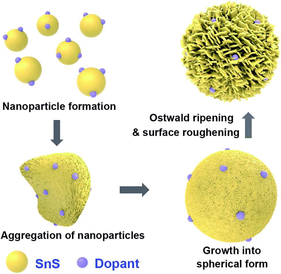
A general schematic of the synthesis process of SnS microspheres is provided in Fig. 1. FESEM observation was performed to investigate the sequence of particle growth and structural evolution at different time intervals during the hydrothermal reaction, i.e. 4, 30, 120, and 180 min, respectively (Fig. 2a–d). As shown in Fig. 2a, microsphere formation started with the formation of nanoparticles. These nanoparticles aggregated to form rough-textured microspheres by a process of oriented aggregation. Here, oriented aggregation refers to the crystal growth phenomenon where primary nanoparticles first self-assemble, then undergo crystallographic reorganization to give rise to the secondary particles of underdeveloped spheres, as captured in Fig. 2b.26
 |
| | Fig. 1 Schematic illustration of synthesis of SnS microspheres. | |
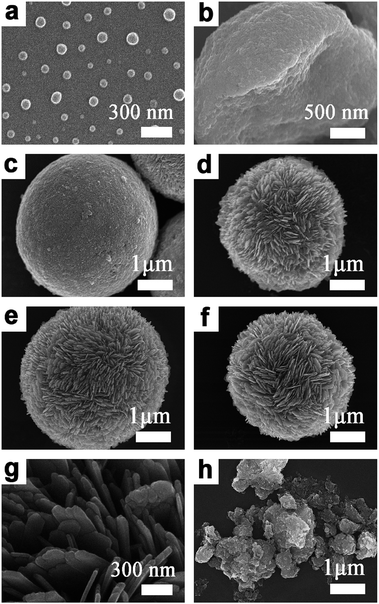 |
| | Fig. 2 FESEM images of (a) 4 min SnS (b) 30 min SnS, (c) 120 min SnS, (d) 180 min 1:1 SnS (e) 1.1:1 SnS, (f) 1.2:1 SnS, (g) high magnification SEM image of 1.1:1 SnS and (h) 1.1:1 SnS without PVP. | |
As the reaction proceeded, particle size increased, and complete spheres were obtained, as shown in Fig. 2c. With further prolonging of the reaction, the surface morphology of particles changed because of the difference in energy between the exterior and interior of the particles; the outer region had greater surface energy and was therefore less stable than the inner part. The surface region therefore preferentially dissolved into solution and the resulting Ostwald ripening process resulted in formation of rough-textured microspheres, as shown in Fig. 2d.25,27 The effect of self-doping on particle morphology and shape was also investigated. Self-doping appeared to have little effect on the shape or morphology of the microparticles that were obtained, as can be seen in Fig. 2d–f. Notably, as revealed in Fig. 2g, the surfaces of the microspheres were completely covered with incorporated nanoplatelets. Additional experimental results performed in the absence of PVP clearly demonstrated the role of PVP as a shaping agent (see Fig. 2h).28
3.2. Material characterization
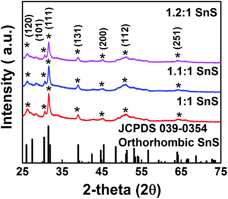
We investigated the crystallographic structure of tin sulfide (SnS) using XRD data (Fig. 3). The peak positions of all samples were in accordance with JCPDS 039-0354 for orthorhombic SnS.14 The 2θ peaks at 26, 31, and 51° were indexed to the (120), (111), and (112) planes of orthorhombic SnS. Smaller peaks corresponding to the face-centred cubic (FCC) planes of orthorhombic SnS were also observed. In particular, no peaks for other phases, such as Sn2S3 or SnS2, were observed. Therefore, the XRD data unambiguously confirmed the formation of tin sulfide (SnS). Furthermore, for the doped samples (1.1:1 SnS and 1.2:1 SnS), there was no change in peak positions or formation of new peaks, supporting no significant difference in crystallography of the parent material after doping. Crystallite size of all samples was calculated from (111) FCC of SnS using the Scherrer equation (Table S1†). Crystallite size decreased slightly in response to doping, although the change in crystallite size did not appear to depend on the doping level.10
 |
| | Fig. 3 XRD of all samples. | |
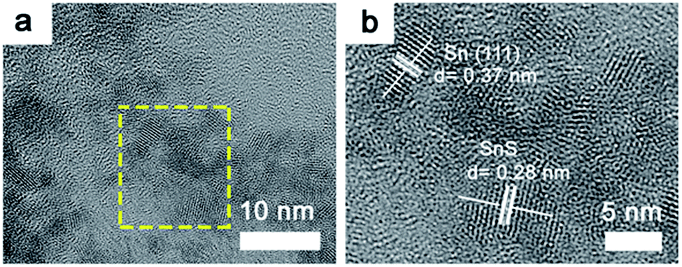
High resolution TEM observation was performed to investigate the presence of dopant sites in the tin sulfide samples. TEM images of 1.1:1 SnS are provided in Fig. 4a and b. Sn dopant sites within the matrix of SnS were clearly identifiable. Lattice spacings of 0.37 nm and 0.28 nm correspond to Sn (111) (JCPDS 01-086-2266) and SnS (111), respectively. The lattice spacing calculated for SnS is in accordance with the XRD results. To explicate the chemical state and composition of tin sulfide, XPS characterization was performed. As shown in Fig. 5a, the low energy spectrum confirmed the presence of Sn and S in the photocatalyst material. The high-resolution spectrum of Sn 3d (Fig. 5b) exhibited two main doublet spin orbit peaks at 486 eV and 494 eV corresponding to Sn2+ 3d5/2 and Sn2+ 3d3/2, respectively.29,30 Furthermore, the Sn 3d peaks were slightly shifted to a lower energy, which confirmed Sn2+ doping (Fig. S1†).31 Similarly, as shown in Fig. 5c, S 2p showed two peaks at binding energies of 160.9 eV and 161.9 eV. Valence band XPS spectra (VB-XPS) near the Fermi level were obtained to investigate the electronic structure of doped SnS (Fig. 5d); the valence band edge for 1.1:1 SnS was 1.43 eV.
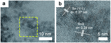 |
| | Fig. 4 (a) TEM image of 1.1:1 SnS, and (b) high magnification TEM image of 1.1:1 SnS. | |
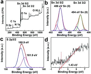 |
| | Fig. 5 (a) Survey XPS spectrum of 1.1:1 SnS. (b) Core level Sn 3d spectra. (c) Core level XPS spectra of S 2p3/2. (d) VB-XPS spectra of 1.1:1 SnS (Sn2+ doped). | |
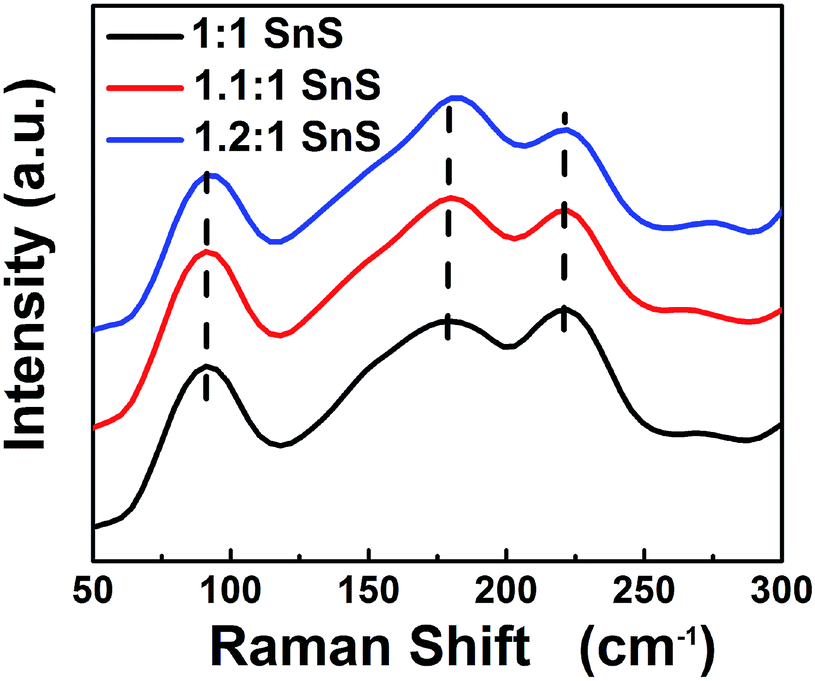
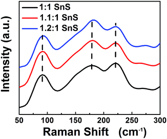
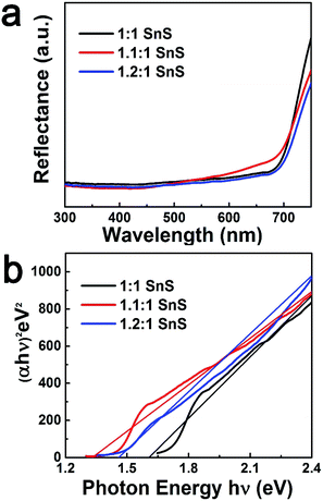
Next, BET surface area was measured and results are tabulated in the ESI (Fig. S2 and Table S2†). BET surface area increased slightly with doping, presumably due to doping facilitating the Ostwald ripening process. Raman spectroscopic analysis was also carried out to confirm the successful formation of SnS and the effect of Sn2+ self-dopant (Fig. 6). Three main peaks were observed at 91, 178 and 221 cm−1 for undoped SnS; the first peak corresponded to Ag mode and the other two peaks corresponded to B1u mode.32,33 A peak shift was clearly observed for the Sn2+ doped samples, confirming successful doping with Sn2+. To calculate the band gap of the synthesized materials, the Kubelka–Munk equation was applied to UV-diffuse reflectance spectroscopy (UV-DRS) data as shown in Fig. 7 using eqn (1):
| | |
F(R) = (1 − R)2/(2R) = α/s
| (1) |
where
F(
R) is the Kubelka Munk function, ‘
R’ is reflectance, ‘
α’ is the absorption coefficient, and ‘
s’ is the scattering coefficient. The scattering coefficient,
s, can be ignored on the basis of wavelength dependence, which makes
F(
R) proportional to
α.
34 Tauc, Davis and Mott proposed an equation to calculate the band gap using the absorption coefficient as follows:
35,36| | |
(hνα)1/n = A(hν − Eg)
| (2) |
 |
| | Fig. 6 Raman Spectrum of all samples. | |
 |
| | Fig. 7 UV-DRS spectrum according to Kubelka–Munk equation of all samples. | |
Here, n = 1/2 for direct band semiconductors and n = 2 for indirect band semiconductors. h is Planck's constant, ν is vibration frequency, and Eg is band gap. By substituting n = 1/2 and α = F(R) into eqn (2), the band gap was calculated by extrapolation of (hνα)2 vs. hν, as shown in Fig. 7b. The estimated band gaps of the synthesized materials (Table 1) were close to the reported values (Table 2). Furthermore, the valence band potential and the conduction band potential were calculated from valence band spectra (VB-XPS) and Eg. With Sn2+ doping, there was a prominent change in the conduction band position. This may have originated from the formation of a discrete energy state below the conduction band that decreased the photonic excitation energy required for charge carrier transition.24 Accordingly, the band gap would have decreased, explaining why Sn2+ doping improved photocatalytic performance. However, when the Sn2+ dopant concentration further increased, the band gap increased slightly, though it was still lower than that of the parent un-doped SnS. A plausible reason for this observation is the Burstein-most effect, which states that the Fermi level shifts above the conduction band once the density of states in the conduction bands are populated.37
Table 1 Estimated band gap, conduction band (CB), and valence band (VB) positions of all samples
| Samples |
Estimated band gap (eV) |
Estimated CB position vs. NHE (eV) |
Estimated VB position vs. NHE (eV) |
| 1:1 SnS |
1.6 |
−0.19 |
1.41 |
| 1.1:1 SnS |
1.32 |
0.11 |
1.43 |
| 1.2:1 SnS |
1.45 |
−0.01 |
1.44 |
Table 2 Report band gap values (eV) of SnS
| Band gap (eV) |
Reference |
| 1.24 |
14 |
| 1.32 |
38 |
| 1.43 |
39 |
| 1.60 |
40 |
3.3. Photocatalytic performance
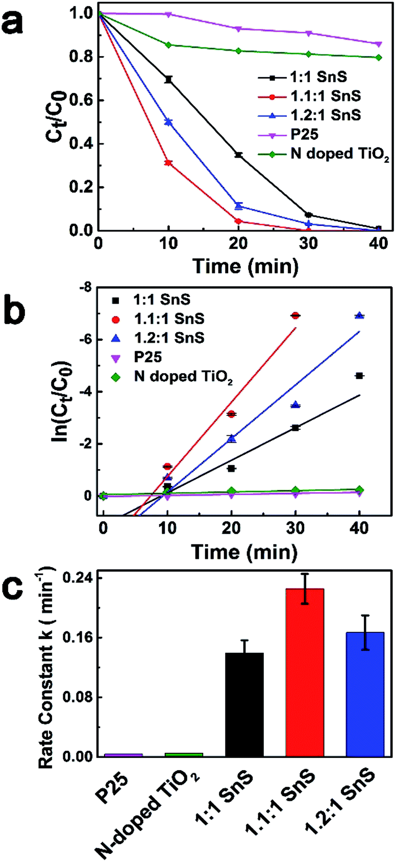
To investigate the photocatalytic performance of synthesized samples, Cr(VI) reduction experiments were performed for Cr(VI) solution at a concentration of 15 ppm using a solar light simulator as the light source. Fig. 8a shows the photoreduction of Cr(VI) with different photocatalysts under ambient temperature and pressure. For comparison, conventional TiO2 nanoparticles of P25, N-doped TiO2, and 1:1 SnS (undoped SnS) were used as reference photocatalyst materials. Citric acid was used as the hole scavenger species.25 C0 is the concentration of Cr(VI) after reaching equilibrium in the dark. As can be seen in in Fig. 8a, P25 and N-doped TiO2 showed very poor catalytic performance with only 13% and 20% reduction in 40 min, respectively, whereas the catalytic efficiency of the undoped SnS sample was better than that of the other two reference materials. Efficiency of the Sn2+ self-doped samples was high; ∼100% reduction within 30 min of irradiation. Therefore, Sn2+ self-doped samples showed significantly better reduction performance than undoped SnS. As can be seen in Fig. 7c the reaction rates increased to 0.2274 min−1 and 0.1661 min−1 for self-doped samples (1.1:1 SnS and 1.2:1 SnS, respectively), whereas the reaction rate was lower for the undoped sample (0.13944 min−1). Here, the increased reduction efficiency obtained for the Sn2+ self-doped SnS can be attributed to the dual role of the self-dopant. First, self-doping increased the charge separation barrier for suppressing electron–hole recombination by providing charge trap sites, and secondly, self-doping decreased the band gap on the electronic scale. Doping generally creates trap sites, and their numbers increase with increasing dopant concentration, favouring photocatalytic performance while minimizing the electron–hole recombination rate. Similarly, a decrease in the band gap usually occurs because of the creation of intermediate energy states within the forbidden gap, thus decreasing the excitation energy reduction efficiency reached a maximum under an optimally adjusted self-doping concentration of 1.1:1 SnS. Further increases in self-dopant concentration decreased the reduction efficiency, as shown for the 1.2:1 SnS sample. This may be because the dopant concentration exceeded an optimum value, increasing the number of trap sites within one particle and consequently decreasing the distance between trap sites, resulting in population of charge recombination sites rather than generation of intrinsic charge trap sites.41 A second reason to explain this observation may be the change in band gap; band gap increased slightly from 1.32 eV to 1.45 eV for 1.2:1 SnS. Digital photographic image showing visible identification of Cr(VI) reduction to Cr(III) using a sample of the doped SnS is provided in Fig. S3.† To further investigate 1.1:1 SnS sample as the most optimal dopant concentration, two more samples with different concentrations (1.05:1.1 SnS and 1.5:1 SnS) were prepared and investigated for photocatalytic activity as shown in Fig. S4.† As a result, sample with 1.1:1 SnS showed the best performance. Recently, there has been a study using Sn4+ self-doped SnS for Cr(VI) reduction, wherein the ratio between Cr(VI) ion and photocatalyst amount (0.02) is nearly the same with the present study. In that work, there reported the presence of SnS2/SnS heterojunctions along with doping sites, which is clearly discerned from this work. Apart from this difference, with regard to the photocatalytic activity, the present system has shown superior performances in reducing Cr(VI) ions.42
Reduction of Cr(VI) via photocatalytic reaction is well understood and had been widely investigated.43,44 Visible light excites the electrons of the catalyst material, which eventually attack the dichromate group (Cr2O72−) to reduce Cr(VI) to Cr(III). Meanwhile, the holes generated as a result of this photoexcitation are consumed by citric acid, which functions as a hole scavenger in this system. The reaction mechanism can be explained as
| | |
4Cr2O72− + C6H5O73− + 41H+ + 6e− → 8Cr3+ + 6CO2 + 23H2O
| (3) |
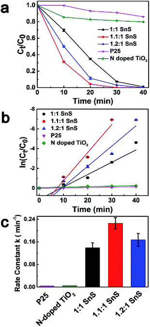 |
| | Fig. 8 Photoreduction of Cr(VI) under visible light irradiation. (a) Ct/C0 concentration changes of Cr(VI) as a function of time using different catalysts. (b) Logarithmic concentration ratio of the samples as a function of time with different catalysts. (c) Bar plot showing the differences in rate constants. | |
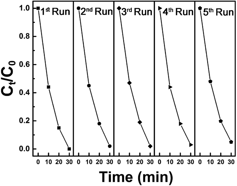
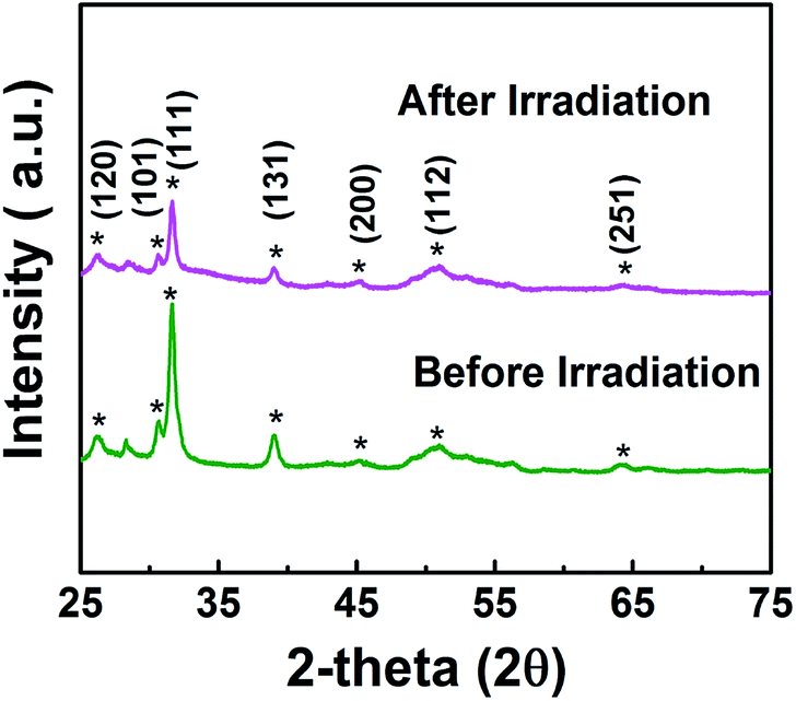
In addition, synthesized samples of doped SnS were checked for their reusability and stability. As shown in Fig. 9, photocatalytic performance was mostly retained after five cycles. The stability of self-doped SnS to irradiation was also investigated through XRD; irradiation did not affect the crystallography of the materials as shown in Fig. 10. In order to investigate further potential of the synthesized material for highly concentrated condition of Cr(VI), 50 ppm of Cr(VI) was also tested for a reduction reaction and the results are provided in Fig. S5.† It has shown considerably good performance with a reduction efficiency of 81% in 50 min of light irradiation.
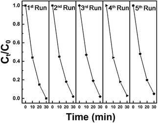 |
| | Fig. 9 Five cycles of photoreduction of Cr(VI) using 1.1:1 SnS as a photocatalyst under visible light irradiation for 30 minutes. | |
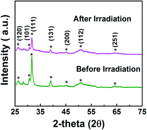 |
| | Fig. 10 XRD of 1.1:1 SnS (doped SnS) sample before and after irradiation. | |
3.4. Photoluminescence measurements
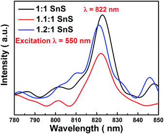
Electron hole recombination rate was characterized using photoluminescence, as shown in Fig. 11. The peak intensity of the emission peak in the PL spectra has a direct relation to the electron hole recombination rate. For this analysis, excitation was done at 550 nm. A clear sharp peak emerged at 822 nm, which is a characteristic peak of SnS. Furthermore, the position of the emission peak directly corresponded to the band gap of SnS, i.e. 1.6 eV as calculated from UV-vis spectrophotometry. The peak intensity varied in the same manner as the changes in photocatalytic activity. Maximum electron–hole recombination rate was observed for undoped SnS (1:1 SnS). With Sn2+ self-doping, the electron–hole recombination rate was supressed, as can be seen from the lower peak intensities in the PL spectra of the self-doped samples (1.1:1 SnS and 1.2:1 SnS). The minimum electron–hole recombination rate was observed at the optimum self-doping concentration of 1.1:1 SnS. The minimum electron–hole recombination rate depends on the number of trap sites, as described in the previous section. A slight peak shift was observed, which may have been due to an increase in the amount of self-dopant.
 |
| | Fig. 11 PL spectrum of different samples excited at 550 nm. | |
3.5. Energy band diagram
Finally, to further confirm the formation of intermediate energy state in the forbidden energy gap, conduction band position was studied as a function of flat band potential. As shown in Fig. 12a, Mott–Schottky method was employed for this purpose. It can be seen that the synthesized doped and un-doped SnS typically exhibit n-type semiconductor characteristics with a positive slope. Moreover, flat band position changes according to doping treatment. It can be deduced that doping would result in a creation of intermediate energy state, which is also indicated by a change in the band gap and VB-XPS. The flat band potential is considered to be approximately equal to the conduction band potential.45 A change in the flat band potential also implies a concurrent change in the conduction band potential. For a undoped (1:1 SnS) sample, the value of the flat band potential (VFB) is equal to −0.79 V, whereas in the case of self-doped SnS (1.1:1 SnS) VFB shifts to −0.75 V. Hence, the formation of intermediate energy state is well verified using Mott–Schottky method.
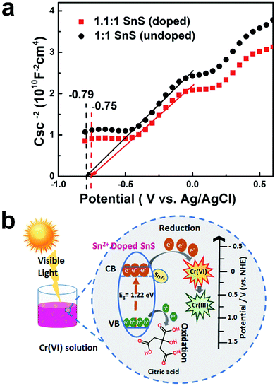 |
| | Fig. 12 (a) Mott–Schottky plots of 1:1 SnS and 1.1:1 SnS (b) energy band diagram of self-doped SnS. | |
Energy band diagrams for Cr(VI) reduction for the doped sample are presented in Fig. 12b. This highlights the role of doping in enhancing the photocatalytic activity of SnS. The effects of doping on the conduction band position and valence band position are described in Table 1. The valence band position was almost identical for all samples. However, the conduction band position changed; for undoped SnS, it was −0.19 eV (vs. normal hydrogen electrode (NHE)), whereas for doped SnS (1.1:1 SnS) it was 0.11 eV (vs. NHE), as shown in Table 1. Doping lowered the conduction band edge, consequently narrowing the band gap. In addition to this change, Sn2+ dopant sites formed as a result of doping, and these acted as trapping sites. For doped semiconductors, trapping sites increase the life time of charge carriers till an optimum point. This will eventually facilitate the reduction of Cr(VI). When the photocatalyst was irradiated, electrons travelled from the valence band to the conduction band, as shown in Fig. 12b, and then these electrons travelled from the conduction band of SnS and attacked Cr(VI), reducing it to Cr(III). The leftover holes generated in the valence band of doped SnS were consumed by citric acid. Overall, the Sn2+ self-doped samples were highly effective photocatalysts for the reduction of Cr(VI).
4. Conclusions
In the present study, Sn2+ self-doped SnS microspheres were synthesized by a simple hydrothermal method without using any template. We demonstrated that the non-stoichiometric self-doping scheme presented here is efficient and straightforward compared to external or impurity-based doping methods. The synthesized Sn2+ self-dopant SnS was used as a photocatalyst for the reduction of toxic Cr(VI) to Cr(III), and showed superior performance to undoped SnS and other reference photocatalysts. The Sn2+ self-dopant enhanced photocatalytic performance in two main ways. By creating an energy state near the conduction band of SnS, the self-dopant lowered the band gap of the parent material. The formation of intermediate energy state was also verified using Mott–Schottky method. Second, the Sn2+ self-dopant formed trap sites, minimizing the recombination problem. Improved photocatalytic reduction efficiencies obtained for the self-doped photocatalysts highlights the importance of self-doping in photocatalysts. In future studies, it is anticipated for exploring self-doped semiconductors as platforms for various electrochemical applications.
Acknowledgements
This work was supported by research grants of the NRF (2014M3A7B4052200, 2014M3C1A3053035) and Basic Science Research Program (2010-0027955) funded by the National Research Foundation under the Ministry of Science, ICT & Future, Korea.
Notes and references
- C. Karunakaran, S. Kalaivani and P. Vinayagamoorthy, Mater. Express, 2014, 4, 125–134 CrossRef CAS.
- L. Ma, L. Xu, X. Xu, X. Zhou and L. Zhang, NANO, 2016, 11, 1650035 CrossRef CAS.
- G. Liu, L. Wang, H. G. Yang, H.-M. Cheng and G. Q. (Max) Lu, J. Mater. Chem., 2010, 20, 831–843 RSC.
- V. B. R. Boppana and R. F. Lobo, J. Catal., 2011, 281, 156–168 CrossRef CAS.
- M. Xing, J. Zhang, F. Chen and B. Tian, Chem. Commun., 2011, 47, 4947–4949 RSC.
- M. Sun, Y. Su, C. Du, Q. Zhao and Z. Liu, RSC Adv., 2014, 4, 30820–30827 RSC.
- H. Huang, X. Li, J. Wang, F. Dong, P. K. Chu, T. Zhang and Y. Zhang, ACS Catal., 2015, 5, 4094–4103 CrossRef CAS.
- F. Zuo, L. Wang, T. Wu, Z. Zhang, D. Borchardt and P. Feng, J. Am. Chem. Soc., 2010, 132, 11856–11857 CrossRef CAS PubMed.
- L. Chen, D. Meng, X. Wu, A. Wang, J. Wang, Y. Wang and M. Yu, J. Phys. Chem. C, 2016, 120, 18548–18559 CAS.
- C.-M. Fan, Y. Peng, Q. Zhu, L. Lin, R.-X. Wang and A.-W. Xu, J. Phys. Chem. C, 2013, 117, 24157–24166 CAS.
- A. Fujushima and K. Honda, Nature, 1972, 238, 37–38 CrossRef.
- S. Chen and L. W. Wang, Chem. Mater., 2012, 24, 3659–3666 CrossRef CAS.
- A. Tanuševski and D. Poelman, Sol. Energy Mater. Sol. Cells, 2003, 80, 297–303 CrossRef.
- J. Chao, Z. Wang, X. Xu, Q. Xiang, W. Song, G. Chen, J. Hu and D. Chen, RSC Adv., 2013, 3, 2746–2753 RSC.
- K. T. Ramakrishna Reddy, N. Koteswara Reddy and R. W. Miles, Sol. Energy Mater. Sol. Cells, 2006, 90, 3041–3046 CrossRef CAS.
- J. J. Loferski, J. Appl. Phys., 1956, 27, 777–784 CrossRef CAS.
- P. Sinsermsuksakul, R. Chakraborty, S. B. Kim, S. M. Heald, T. Buonassisi and R. G. Gordon, Chem. Mater., 2012, 24, 4556–4562 CrossRef CAS.
- D. Das and R. K. Dutta, J. Colloid Interface Sci., 2015, 457, 339–344 CrossRef CAS PubMed.
- Z. Fang, Q. Wang, X. Wang, F. Fan, C. Wang and X. Zhang, Mater. Res. Bull., 2013, 48, 4935–4941 CrossRef CAS.
- Y. Zhang, J. Lu, S. Shen, H. Xu and Q. Wang, Chem. Commun., 2011, 47, 5226–5228 RSC.
- H. Li, T. Wu, B. Cai, W. Ma, Y. Sun, S. Gan, D. Han and L. Niu, Appl. Catal., B, 2015, 164, 344–351 CrossRef CAS.
- H.-T. Hsu, S.-S. Chen, W.-S. Chang and C.-W. Li, Desalin. Water Treat., 2013, 51, 495–502 CrossRef CAS.
- C. D. Pereira, J. G. Techy, E. M. Ganzarolli and S. P. Quináia, J. Environ. Monit., 2012, 14, 1559–1564 RSC.
- F. Xie, X. Mao, C. Fan and Y. Wang, Mater. Sci. Semicond. Process., 2014, 27, 380–389 CrossRef CAS.
- A. Rauf, M. S. A. Sher Shah, G. H. Choi, U. Bin Humayoun, D. H. Yoon, J. W. Bae, J. Park, W.-J. Kim and P. J. Yoo, ACS Sustainable Chem. Eng., 2015, 3, 2847–2855 CrossRef CAS.
- V. M. Yuwono, N. D. Burrows, J. A. Soltis and R. L. Penn, J. Am. Chem. Soc., 2010, 132, 2163–2165 CrossRef CAS PubMed.
- X.-J. Dai, Y.-S. Luo, W.-D. Zhang and S.-Y. Fu, Dalton Trans., 2010, 39, 3426–3432 RSC.
- K. M. Koczkur, S. Mourdikoudis, L. Polavarapu and S. E. Skrabalak, Dalton Trans., 2015, 44, 17883–17905 RSC.
- W. Xia, H. Wang, X. Zeng, J. Han, J. Zhu, M. Zhou and S. Wu, CrystEngComm, 2014, 16, 6841–6847 RSC.
- C.-H. Cheng, Y.-C. Chi, C.-L. Wu, C.-J. Lin, L.-H. Tsai, J.-H. Chang, M. K. Chen, M.-H. Shih, C.-K. Lee, C.-I. Wu, D. P. Tsai and G.-R. Lin, Nanoscale, 2016, 8, 4579–4587 RSC.
- H. Wang, X. Lu, J. Tucek, J.-G. Zheng, G. Yang, R. Zboril and C. Niu, Electrochim. Acta, 2016, 211, 636–640 CrossRef CAS.
- M. Patel, A. Chavda, I. Mukhopadhyay, J. Kim and A. Ray, Nanoscale, 2016, 8, 2293–2303 RSC.
- H. R. Chandrasekhar, R. G. Humphreys, U. Zwick and M. Cardona, Phys. Rev. B: Condens. Matter Mater. Phys., 1977, 15, 2177–2183 CrossRef CAS.
- H. Kisch, Semiconductor Photocatalysis: Principles and Applications, Wiley-VCH verlag GmbH & Co. KGaA, 2015 Search PubMed.
- A. Tauc, J. Grigorovici and R. Vancu, Mater. Res. Bull., 1966, 3, 37–46 CrossRef.
- E. a. Davis and N. F. Mott, Philos. Mag., 1970, 22, 0903–0922 CrossRef CAS.
- S. State, O. Ridge and O. Ridge, Phys. Rev. B: Condens. Matter Mater. Phys., 1988, 37, 244–248 Search PubMed.
- N. Koteeswara Reddy and K. T. Ramakrishna Reddy, Mater. Chem. Phys., 2007, 102, 13–18 CrossRef.
- B. Ghosh, M. Das, P. Banerjee and S. Das, Appl. Surf. Sci., 2008, 254, 6436–6440 CrossRef CAS.
- N. Sato, M. Ichimura, E. Arai and Y. Yamazaki, Sol. Energy Mater. Sol. Cells, 2005, 85, 153–165 CrossRef CAS.
- W. Choi, A. Termin and M. R. Hoffmann, J. Phys. Chem., 1994, 98, 13669–13679 CrossRef.
- Q. Xie, H. Zhou, Z. Lv and H. Guo, J. Mater. Chem. A, 2017, 5, 6299–6309 CAS.
- P. Mohapatra, S. K. Samantaray and K. Parida, J. Photochem. Photobiol., A, 2005, 170, 189–194 CrossRef CAS.
- J. M. Meichtry, M. Brusa, G. Mailhot, M. A. Grela and M. I. Litter, Appl. Catal., B, 2007, 71, 101–107 CrossRef CAS.
- D. Xu, B. Cheng, S. Cao and J. Yu, Appl. Catal., B, 2015, 164, 380–388 CrossRef CAS.
Footnote |
| † Electronic supplementary information (ESI) available. See DOI: 10.1039/c7ra03854b |
|
| This journal is © The Royal Society of Chemistry 2017 |
Click here to see how this site uses Cookies. View our privacy policy here. 
 Open Access Article
 This Open Access Article is licensed under a
  a,
Md. Selim Arif Sher Shah
a,
Md. Selim Arif Sher Shah