
 Open Access Article
 This Open Access Article is licensed under a
 Creative Commons Attribution 3.0 Unported Licence
Tunable electronic properties of arsenene/GaS van der Waals heterostructures†
Xiao-Hua Lia,
Bao-Ji Wang *a,
Xiao-Lin Caia,
Li-Wei Zhanga,
Guo-Dong Wanga and
San-Huang Ke*b
*a,
Xiao-Lin Caia,
Li-Wei Zhanga,
Guo-Dong Wanga and
San-Huang Ke*b
aSchool of Physics and Electronic Information Engineering, Henan Polytechnic University, Jiaozuo 454000, China. E-mail: wbj@hpu.edu.cn
bMOE Key Laboratory of Microstructured Materials, School of Physics Science and Engineering, Tongji University, Shanghai, 200092, China. E-mail: shke@tongji.edu.cn
First published on 1st June 2017
Abstract
Finding novel atomically thin heterostructures and understanding their electronic properties is critical for developing better nanoscale electronic and optoelectronic devices. In this work, we investigate the structural and electronic properties of arsenene/GaS van der Waals (vdW) heterostructures using first-principles calculations. Our results suggest that this heterostructure has an intrinsic type-II band alignment and an indirect band gap. Comparing the calculated band edge positions to the redox potentials of water, we identify that the arsenene/GaS vdW heterostructure is a promising photocatalyst for water splitting. Moreover, we also find that intriguing indirect–direct and semiconductor–metal transitions can be induced by strain. In particular, under certain strain, degenerate valleys of conduction band bottoms will be created, which suggests potential applications in valleytronics.
1 Introduction
Since the successful isolation of graphene, great attention have been paid to the research into new two-dimensional (2D) materials. To date, many new graphene-like 2D materials, such as boron nitride,1 transition metal dichalcogenides (TMDCs),2 phosphorene,3,4 and others5–7 have been widely studied due to their interesting physical properties and promising applications.6,7 Among these, GaS monolayer recently received extensive attention because it has successfully been fabricated by mechanical exfoliation from the bulk or vapor transport techniques.5,8,9 Theoretical calculations based on density functional theory (DFT) have shown that a GaS monolayer is an indirect-band-gap semiconductor and is suitable for photocatalytic water splitting.10,11 Besides, monolayer gray arsenic (arsenene) – a new elemental 2D semiconducting material with buckled honeycomb lattice, has been proposed and predicted to be kinetically very stable based on the theoretical calculations.12,13 It is also found that arsenene is an indirect-band-gap semiconductor and undergoes an indirect–direct and semiconducting–metallic transitions under external electric fields or strains.12,13As is well known, heterostructures and interfaces of semiconducting materials often play a more crucial role in electronic and photonic nanodevices than the bulks.14 2D materials just offer a platform that allows creation of van der Waals (vdW) heterostructures with a variety of properties, where one layered 2D structure is stacked on another by vdW forces.15 Recently, various vertically-stacked vdW heterostructures have been realized experimentally and utilized to make electronic and optoelectronic devices with novel physical properties and distinctive capabilities.16–18 At the same time, many theoretical researchers have also shifted their focus from monocomponent systems to vdW heterostructures. For instance, a theoretical study demonstrated that the electronic properties of GaS/GaSe heterostructures with an indirect band gap can be continuously tuned by external strain.19 In the case of silicene/GaS heterostructures, it was found that the interlayer charge redistribution can open a sizable gap at the Dirac point, which can be further modulated by bias voltages and strains.20 Work by Su et al. showed that the indirect band gap of arsenene/MoS2 heterostructure is tunable by changing the interlayer distance.21 A first-principles study of the electronic properties of arsenene/graphene heterostructures showed that varying the interlayer distance can not only control Schottky barriers but also control Schottky contacts of the vdW heterostructures.22 All these findings suggest that stacking two 2D materials into vdW heterostructures provides an effective way to design novel artificial materials with special characteristics. This motivates us to consider the two newly found 2D materials – arsenene and GaS monolayer which have very close lattice constants, and to see whether they can form a stable arsenene/GaS (A/G) vdW heterostructure and what interesting electronic properties it can provide. In this work, by performing first-principles calculations, we first identify the equilibrium geometry of the stable A/G vdW heterostructure. Then we investigate its electronic properties, including the projected band structures, band alignments, as well as the charge transfer. In addition, the strain modulation of the electronic properties is also studied. The present work is beneficial to the future realization of A/G devices used in nanoelectronics and/or optoelectronics.
2 Computational methods
All the calculations performed in this work are based on DFT as implemented in the Vienna ab initio simulation package (VASP).23 The projector augmented wave method (PAW) is used to describe the ion–electron interactions.24 The electron exchange and correlation are treated by the generalized gradient approximation (GGA) in the version of Perdew–Burke–Ernzerhof (PBE),25 and by the hybrid functional method in the version of Heyd–Scuseria–Ernzerhof (HSE06) which has been proven to be able to obtain band gaps closer to experimental values for semiconductors.26 The DFT-D2 correction of Grimme is adopted to describe the interlayer vdW interaction,27 which has been evidenced to give reliable descriptions for various vdW heterostructures19–22,28 and layered compounds such as arsenic.29 Plane waves with a kinetic energy cutoff of 500 eV are used to expand the wave functions. The reciprocal space is sampled with a fine k-point mesh of 11 × 11 × 1 in the irreducible Brillouin zone. A vacuum spacing of 15 Å is adopted to eliminate the artificial interactions between the periodic imagines. Test calculations show that the above parameters converge the results very well. The atomic structures (including the lattice constants) of the systems considered are fully relaxed by minimizing the stresses and the atomic forces acting on each atoms to be less than 0.01 eV Å−1 within the conjugate gradient algorithm. Atomic charge transfers are determined by Bader's charge analysis.303 Results and discussions
We first check the lattice constants of pristine arsenene and GaS monolayers using DFT/PBE. The results are 3.61 and 3.63 Å for arsenene and GaS, respectively, which are in good agreement with previous results.10,12,13,29 The very small lattice mismatch (∼0.55%) makes it easy to form heterostructures. Here, we choose the lattice constant of GaS to be the lattice constant of the heterostructure, which corresponds to the epitaxial growth of arsenene on a GaS substrate in experiment. The monolayer arsenene and GaS can form three different heterostructures in terms of their stacking conformation: AA, ABS, and ABGa stacking, as shown in Fig. 1(a)–(c), respectively. In the AA stacking, the As atoms of the two sublattices are located on the top of Ga or S atoms. While in the ABS (ABGa) stacking, one As sublattice is on the top of the S(Ga) sublattice and the other one is on the top of the hexagonal center. To compare the relative stability of these heterostructures, we calculate their interface binding energies, Eb = EH − WA − EG, where EH, EA, and EG represent the total energy of the A/G heterostructure, arsenene, and GaS monolayer, respectively. By this definition, a lower Eb value means better stability of the heterostructure. The results in Fig. 1(d) show that the ABS stacking with an equilibrium interlayer distance of 3.05 Å is the most stable one whose binding energy is −0.17 eV per unit, being comparable to other vdW systems.19,31,32 To further check the dynamic stability of this structure, we perform phonon spectra calculation and show the result in Fig. 1(e). One can see that all phonon modes have positive frequencies except for the transverse acoustic mode near the Γ point. This mode gets negative frequencies due to the phonon softening.33 Our result confirms overall the dynamic stability of the system. In the following, we only consider the heterostructure in the ABS stacking. | ||
| Fig. 1 Top and side views of (a) AA-, (b) ABS-, (c) ABGa-stacking A/G heterostructures. The blue dashed rhombus indicates the unit cell. As, Ga, and S atoms are represented by pink, seagreen, and yellow balls, respectively. The arrows indicate the interlayer distance d between the arsenene and GaS layers. (d) Binding energy per unit cell of the A/G heterostructures as a function of d. (e) Phonon spectra of the ABS-stacking A/G heterostructure. | ||
We perform more accurate DFT/HSE06 calculations to investigate the electronic properties of the A/G vdW heterostructure. As a reference, the band structures of arsenene and GaS monolayers are also calculated and plotted in Fig. 2(a) and (b), respectively. It shows that the two monolayers are both indirect-band gap semiconductors, and the band gaps are 2.21 and 3.24 eV for arsenene and GaS monolayers, respectively, which agree well with previous theoretical results.10,13,29 The projected band structure of the heterostructure is given in Fig. 2(c), in which the red and green circles indicate the contributions from the arsenene and GaS layers, respectively. As one can see, the A/G heterostructure is a semiconductor with an indirect band gap of 2.09 eV. Its valence band maximum (VBM) is mainly contributed from arsenene while its conduction band minimum (CBM) is predominately ascribed to GaS, indicating that a type-II heterostructure is formed. This is consistent with a type-II band alignment between arsenene and GaS, as shown schematically in Fig. 2(f) (see later discussion). The total and partial density of states (PDOSs) plotted in Fig. 2(d) show that the VBM is mainly dominated by the 4p states of As atoms, while the CBM mainly originates from the 3p states of S atoms and 4s, 4p, and 3d states of Ga atoms. This is consistent with the decomposed charge densities of the VBM and CBM in Fig. 2(e), which show that the VBM is from As atoms while the CBM is from Ga and S atoms. We note that the VBM largely consists of the lone-pair pz orbitals of arsenene, which induce the formation of π-bond-like states in the interlayer region and are beneficial to make the two monolayers stay closer.21,34
 | ||
| Fig. 2 Band structures given by DFT/HSE06 of (a) arsenene, (b) GaS monolayer, and (c) A/G heterostructure. The Fermi level is set as zero. The solid arrows indicate the indirect band gaps. (d) Total and partial density of states of the A/G heterostructure, given by DFT/HSE06 calculations. (e) Band decomposed charge densities of the VBM and CBM of the A/G heterostructure. (f) Band alignment of the A/G heterostructure. The vacuum level is taken as a reference. | ||
The band alignments of the A/G heterostructure are determined by using the vacuum level as an energy reference. As shown in Fig. 2(f), the band edges of monolayer arsenene and GaS are (−5.76, −3.63) and (−6.96, −3.67) eV, respectively. Arsenene and GaS layers form a type-II heterostructure with a work function of 5.51 eV, which will spontaneously separate the free electrons and holes, enabling high efficiency optoelectronics and solar energy conversion. Interestingly, our calculations demonstrate that the energies of the CBM and VBM relative to the vacuum level are −3.67 eV and −5.76 eV, respectively, perfectly straddling the redox potential energies (−4.44 to −5.67 eV) of water.35 This implies that the A/G heterostructure is a potential photocatalyst for splitting water. From Fig. 2(e), one can see that when incoming solar photons are absorbed by the A/G heterostructure, the photogenerated electrons will transfer from VBM to CBM, and hence hydrogen and oxygen will be separately produced at the As monolayer and the GaS monolayer during the photocatalytic water splitting.36 To show the water–heterostructure interaction, we further investigate possible adsorption configurations of water molecules on the heterostructures by calculating their adsorption energies at the DFT level (see ESI: Fig. S1 and Table S1†).37 The results show that of all the examined adsorption sites, water molecules favor sitting above the bottom As and S atoms in the one-leg configuration (Fig. S1(c)†). A metastable state, in which the water molecules sit above the hexagonal ring center of arsenene or GaS in the one-leg manner (see Fig. S1(d)†), is available. It should be noted, however, that a direct investigation of the detailed water-splitting process is considerably beyond the scope of this work, which will require much more expensive quantum molecular dynamics (MD) simulations or QMMM MD simulations. We would like to leave this to a future work of quantum MD simulations.
To have a more detailed understanding of the electronic properties of the A/G heterostructure, we plot in Fig. 3(a) the plane-averaged charge density difference along z-direction normal to the heterostructure as Δρ(z) = ρH(z) − ρA(z) − ρG(z), where ρH(z), ρA(z), and ρG(z) are the plane-averaged charge densities of the heterostructure, the pristine arsenene, and the pristine monolayer GaS, respectively. It can be seen that the charge densities around As atoms are no longer equivalent and remarkable charge rearrangement occurs around the interface. Bader charge analyses show that 0.02 electrons per unit are transferred from arsenene to GaS monolayer, indicating an additional electrostatic interlayer coupling besides the vdW interaction. Fig. 3(b) shows the plane-averaged electrostatic potential along z-direction normal to the surface. One can see that the GaS layer has a deeper potential than that of arsenene. This can be understood by considering the different atomic electronegativities (As 2.18, Ga 1.81, S 2.58), making electrons transferred from the arsenene to the GaS layer, as observed. The potential drop (ΔVAs/GaS) across the bilayer is found to be 4.13 eV (see Fig. 3(b)) which implies a strong electrostatic field across the interface. This electric field may significantly influence the carrier dynamics and make the excitonic behavior of A/G heterostructure quite different from that of the isolated GaS layer as it may facilitate the separation of electrons and holes.38
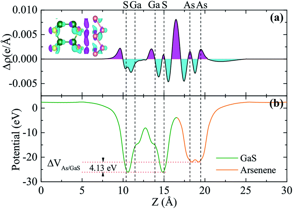 | ||
| Fig. 3 (a) Plane-averaged charge density difference and (b) electrostatic potentials of the A/G heterostructure along z-direction normal to the heterostructure. The inset in (a) is the 3D isosurface of the charge density difference. The magenta and cyan areas represent electron accumulation and depletion, respectively. The vertical dashed lines indicate the positions of the Ga, S, and As atoms in the heterostructure, respectively. | ||
Tunability of electronic properties of a material by external control, such as strain, is very beneficial for its applications in nanoelectronics or optoelectronics.39 Here, we first consider in-layer biaxial strains where the hexagonal unit cell is enlarged or shrunk symmetrically with specific ratios (see the inset of Fig. 4(a)), ε = (L − L0)/L0, where L and L0 are the lattice constants of the strained and unstrained structures, respectively. The band-gap evolution given by the vdW-DFT/PBE under various biaxial strains is shown in Fig. 4(a) together with the strain energy. One can see that the band gap decreases with the increase in either compressive or tensile strain, and the system will become metallic for strains beyond ±10%. We note that DFT/PBE usually underestimates band gaps of semiconductors because of the lacking of derivative discontinuity in the energy functional. However, our purpose here is to see the trend in band gap variation under different strains instead of the absolute values of band gap, therefore the results can still be expected to be meaningful. This justification is also supported by previous calculations using the PBE functional and the hybrid functional HSE06, showing consistent strain-induced effects on band structures.40
 | ||
| Fig. 4 (a) Calculated strain energy and band gap by DFT/PBE + vdW as functions of the in-layer biaxial strain for the A/G heterostructure. The inset shows the schematic representation of the biaxial strain applied. The evolutions of the highest valence band and the lowest conduction band of the A/G heterostructure under various tensile (b) and compressive (c) biaxial strains. | ||
The dependence of the highest valence and lowest conduction bands on the biaxial strains is respectively shown in Fig. 4(b) and (c), which clearly demonstrate that the size and characteristic of the band-gap is determined by the strain-induced band-energy shifts at different k points. Similar to the HSE06 result, the free-standing heterostructure possesses an indirect band gap between VBM at k1 (0.13, 0.07, 0) and CBM at k2 (0.38, 0, 0), denoted by A and B in Fig. 4(b) or (c), respectively. Under an increasing tensile strain, the VBM is always located at A. However, the energy of the conduction band bottom at Γ-point shifts downwards more rapidly than the original CBM, and they become equal under a tension of 0.3%. For tensile strains larger than 0.3%, the conduction band bottom at Γ-point has a lower energy than B and becomes the new CBM. On the other hand, when an increasing compressive strain is applied, both the conduction and valence bands tend to shift downwards while the valence band top at Γ-point shifts slightly upwards and becomes the new VBM under large compressive strains. The conduction band bottom at K point drops faster than B, and becomes equal in energy to B at ε ≃ −4.5%, and eventually becomes the new CBM when ε > −4.5%. It is interesting to note that there are two critical strains, 0.3% and −4.5%, under which degenerate conduction band valleys are created. This behavior would have potential applications for valleytronic devices: quasiparticles with the same energy at different positions in momentum space are less susceptible to phonon scattering.41,42
To check if all the strains considered are within the elastic limit, we calculate the strain energy per atom, Es = (Estrained − Eunstrained)/n, with n being the number of atoms in the unit cell. The results in Fig. 4(a) (right y-axis) show that Es varies smoothly as a quadratic function of the strain, indicating that the system is flexible and all the strains considered are within the elastic limit and, therefore, are fully reversible.
Besides the in-plane strain modulation of band gap, out-of-plane vertical strains may also provide a means for tuning continuously the band gap.19,43–45 Fig. 5(a) shows the variation of the band gap as a function of the interlayer distance. One can see that the band gap decreases linearly with the interlayer distance decreasing (vertical compressive strains), and its indirect nature is remained even under very large compression, as shown in Fig. 5(b). On the other hand, when the interlayer distance is increased (tensile strains), the band gap first increases slightly and then stays unchanged, indicating a convergence reached, as shown in Fig. 5(c). Similar behavior was also found in GaS/GaSe and As/MoS2 heterostructures.19,21 Here, an interesting indirect–direct transition of band gap occurs under certain vertical tension: when the interlayer distance is larger than 3.5 Å the system has now a direct band gap of ∼1.59 eV at Γ point, which is due to the up-shift of B state and the up-shift of the valence band top at Γ point. In this case, the difference between the Γ–Γ direct and Γ–B indirect gaps is so small that new degenerate valleys occur regardless of the (increased) interlayer distance.
 | ||
| Fig. 5 (a) Calculated band gap of the A/G heterostructure as a function of the interlayer distance. The equilibrium structure is indicated with a black arrow. The evolutions of the highest valence band and the lowest conduction band of the A/G heterostructure with different compressed (b) and extended (c) interlayer distances. The Fermi level is set as zero. | ||
Finally, we would like to point out that the DFT-D2 method, a vdW correction scheme adopting a pairwise semi-empirical approach, completely neglects many-body effects, which may have some effect on the present results.46,47 To examine this effect and the reliability of our results, we further perform test calculations adopting the many-body dispersion energy method (MBD@rsSCS). From the results shown in Fig. S2† one can see that the equilibrium interlayer distances (∼3.05 Å vs. ∼3.10 Å) and the band structures given by DFT-D2 and MBD@rsSCS are almost identical though there is a small difference in the binding energy. This indicates that the present results are reliable and will not be changed qualitatively by the use of different vdW corrections.
4 Conclusions
In summary, by performing first-principles calculations with vdW corrections, we have investigated systematically the structural stability and electronic properties of A/G vdW heterostructures. The dynamic stability of the ABS-stacking A/G heterostructure is demonstrated by its binding energy and phonon spectra. This heterostructure is found to be an indirect-band-gap semiconductor with intrinsic type-II band alignment and is a potential photocatalyst for splitting water. Moreover, the band gap of the A/G heterostructure can be effectively modulated by external strains. An increasing in-layer strain will decrease near linearly the band gap. On the other hand, an increasing vertical compressive strain will reduce the band gap, while an increasing vertical tensile strain will enlarge slightly the band gap. When the interlayer distance is increased to be larger than 3.5 Å the band gap becomes direct (∼1.59 eV) at Γ point. In this case, degenerate valleys of CBM will be created, which suggests potential applications in valleytronics. Our findings show potential applications of the A/G vdW heterostructure in future flexible electronics and optoelectronics.Acknowledgements
This work was supported by the National Natural Science Foundation of China (No. 11174220 and 11374226), the Key Scientific Research Project of the Henan Institutions of Higher Learning (No. 16A140009), the Natural Science Foundation of Henan Province of China (No. 162300410116), the Program for Innovative Research Team of Henan Polytechnic University (No. T2015-3 and T2016-2), and the Doctoral Foundation of Henan Polytechnic University (No. B2015-46), as well as by the High-performance Grid Computing Platform of Henan Polytechnic University.References
- J. Nakamura, T. Nitta and A. Natori, Phys. Rev. B: Condens. Matter Mater. Phys., 2005, 72, 205429 CrossRef.
- Y. F. Li, Z. Zhou, S. B. Zhang and Z. F. Chen, J. Am. Chem. Soc., 2008, 130, 16739 CrossRef CAS PubMed.
- L. Li, Y. Yu, G. J. Ye, Q. Ge, X. Ou, H. Wu, D. Feng, X. H. Chen and Y. Zhang, Nat. Nanotechnol., 2014, 9, 372 CrossRef CAS PubMed.
- H. O. H. Churchill and P. Jarillo-Herrero, Nat. Nanotechnol., 2014, 9, 330 CrossRef CAS PubMed.
- D. J. Late, B. Liu, J. Luo, A. Yan, M. H. S. S. Ramakrishna, M. Grayson, C. N. R. Rao and V. P. Dravid, Adv. Mater., 2012, 24, 3549 CrossRef CAS PubMed.
- Q. Tang and Z. Zhou, Prog. Mater. Sci., 2013, 111, 1244 CrossRef.
- Q. Tang, Z. Zhou and Z. F. Chen, WIREs Computational Molecular Science, 2015, 5, 360 CrossRef CAS.
- G. Z. Shen, D. Chen, P. C. Chen and C. W. Zhou, ACS Nano, 2009, 3, 1115 CrossRef CAS PubMed.
- S. K. Panda, A. Datta, G. Sinha, S. Chaudhuri, P. G. Chavan, S. S. Patil, M. A. More and D. S. Joag, J. Phys. Chem. C, 2008, 112, 6240 CAS.
- V. Zólyomi, N. D. Drummond and V. I. Fal'ko, Phys. Rev. B: Condens. Matter Mater. Phys., 2013, 87, 195403 CrossRef.
- H. L. Zhuang and R. G. Hennig, Chem. Mater., 2013, 25, 3232 CrossRef CAS.
- S. Zhang, Z. Yan, Y. Li, Z. Chen and H. Zeng, Angew. Chem., Int. Ed., 2015, 54, 3112 CrossRef CAS PubMed.
- C. Kamal and M. Ezawa, Phys. Rev. B: Condens. Matter Mater. Phys., 2015, 91, 085423 CrossRef.
- B. Radisavijevic, A. Radenovic, J. Brivio, V. Giacometti and A. Kis, Nat. Nanotechnol., 2011, 6, 147 CrossRef PubMed.
- K. S. Novoselov, A. Mishchenko, A. Carvalho and A. H. C. Neto, Science, 2016, 353, 461 CrossRef CAS PubMed.
- Z. Wu, Y. Zheng, S. H. Zheng, S. Wang, C. L. Sun, K. Parvez, T. Ikeda, X. Bao, K. Müllen and X. Feng, Adv. Mater., 2016, 29, 1602960 CrossRef PubMed.
- M. S. Long, E. F. Liu, P. Wang, A. Y. Gao, H. Xia, W. Luo, B. G. Wang, J. W. Zeng, Y. J. Fu, K. Xu, W. Zhou, Y. Y. Lv, S. H. Yao, M. H. Lu, Y. F. Chen, Z. H. Ni, Y. M. You, X. A. Zhang, S. Q. Qin, Y. Shi, W. D. Hu, D. Y. Xing and F. Miao, Nano Lett., 2016, 15, 2254 CrossRef PubMed.
- D. Li, X. J. Wang, Q. C. Zhang, L. P. Zou, X. F. Xu and Z. X. Zhang, Adv. Funct. Mater., 2015, 25, 7362 Search PubMed.
- W. Wei, Y. Dai, C. W. Niu, X. Li, Y. D. Ma and B. B. Huang, J. Mater. Chem. C, 2015, 3, 11548 RSC.
- Y. Ding and Y. L. Wang, Appl. Phys. Lett., 2013, 103, 043114 CrossRef.
- J. Su, L. P. Feng, H. X. Pana, H. C. Lu and Z. T. Liua, Mater. Des., 2016, 96, 257 CrossRef CAS.
- C. X. Xia, B. Xue, T. X. Wang, Y. T. Peng and Y. Jia, Appl. Phys. Lett., 2015, 107, 193107 CrossRef.
- G. Kresse and J. Hafner, Phys. Rev. B: Condens. Matter Mater. Phys., 1993, 47, 558 CrossRef CAS.
- P. E. Blöchl, Phys. Rev. B: Condens. Matter Mater. Phys., 1994, 50, 17953 CrossRef.
- J. P. Perdew, K. Burke and M. Ernzerhof, Phys. Rev. Lett., 1996, 77, 3865 CrossRef CAS PubMed.
- J. Heyd, G. E. Scuseria and M. Ernzerhof, J. Chem. Phys., 2006, 124, 219906 CrossRef.
- S. Grimme, J. Comput. Chem., 2006, 27, 1787 CrossRef CAS PubMed.
- L. Shi, T. S. Zhao, A. Xua and J. B. Xu, J. Mater. Chem., 2016, 4, 16377 RSC.
- L. Z. Kou, Y. D. Ma, X. Tan, T. Frauenheim, A. J. Du and S. Smith, J. Phys. Chem. C, 2015, 119, 6918 CAS.
- R. F. W. Bader, Atoms in Molecules – A Quantum Theory, Oxford University Press, Oxford, UK, 1990 Search PubMed.
- J. Zhou, Applied Materials Today, 2016, 2, 24 CrossRef.
- E. Torun, H. Sahin and F. M. Peeters, Phys. Rev. B, 2016, 93, 075111 CrossRef.
- H. Şahin, S. Cahangirov, M. Topsakal, E. Bekaroglu, E. Akturk, R. T. S. Adn and S. Ciraci, Phys. Rev. B: Condens. Matter Mater. Phys., 2009, 80, 155453 CrossRef.
- Z. Zhu, J. Guan and D. Tománek, Phys. Rev. B: Condens. Matter Mater. Phys., 2015, 91, 161404 CrossRef.
- H. L. Zhuang, M. D. Johannes, M. N. Blonsky and R. G. Hennig, Appl. Phys. Lett., 2014, 104, 022116 CrossRef.
- J. Liao, B. Sa, J. Zhou, R. Ahuja and Z. Sun, J. Phys. Chem. C, 2014, 118, 17954 Search PubMed.
- J. Ma, A. Michaelides, D. Alfè, L. Schimka, G. Kresse and E. Wang, Phys. Rev. B: Condens. Matter Mater. Phys., 2011, 84, 033402 CrossRef.
- Y. Q. Cai, G. Zhang and Y. W. Zhang, J. Phys. Chem. C, 2008, 119, 13929 Search PubMed.
- J. Li, Z. Shan and E. Ma, MRS Bull., 2014, 39, 108 CrossRef CAS.
- X. Peng, Q. Wei and A. Copple, Phys. Rev. B: Condens. Matter Mater. Phys., 2014, 90, 085402 CrossRef.
- H. L. Zeng, J. F. Dai, W. Yao, D. Xiao and X. D. Cui, Nat. Nanotechnol., 2012, 7, 490 CrossRef CAS PubMed.
- X. Y. Han, H. M. Stewart, S. A. Shevlin, C. R. A. Catlow and Z. X. Guo, Nano Lett., 2014, 14, 4607 CrossRef CAS PubMed.
- M. Dienwiebel, G. S. Verhoeven, N. Pradeep and J. W. M. Frenken, Phys. Rev. Lett., 2004, 92, 126101 CrossRef PubMed.
- S. Tongay, W. Fan, J. Kang, J. Park, U. Koldemir, J. Suh, D. S. Narang, K. Liu, J. Ji, J. B. L. R. S. Sinclair and J. Q. Wu, Nano Lett., 2014, 14, 3185 CrossRef CAS PubMed.
- W. Q. Xiong, C. X. Xia, X. Zhao, T. X. Wang and Y. Jia, Carbon, 2016, 109, 737 CrossRef CAS.
- T. Bučko, S. Lebègue, T. Gould and J. G. Ángyán, J. Phys.: Condens. Matter, 2016, 28, 045201 CrossRef PubMed.
- A. Ambrosetti, N. Ferri, R. A. DiStasio Jr and A. Tkatchenko, Science, 2016, 351, 1171 CrossRef CAS PubMed.
Footnote |
| † Electronic supplementary information (ESI) available. See DOI: 10.1039/c7ra03748a |
| This journal is © The Royal Society of Chemistry 2017 |