
 Open Access Article
 This Open Access Article is licensed under a
 Creative Commons Attribution 3.0 Unported Licence
Nitrogen doping for facile and effective modification of graphene surfaces
A. Yanilmaza,
A. Tomaka,
B. Akbalib,
C. Bacaksizb,
E. Ozceriab,
O. Arib,
R. T. Sengerb,
Y. Selametb and
H. M. Zareie *c
*c
aDepartment of Materials Science and Engineering, Izmir Institute of Technology, Izmir 35430, Turkey
bDepartment of Physics, Izmir Institute of Technology, Izmir 35430, Turkey
cMicrostructural Analysis Unit, School of Physics and Advanced Materials, University of Technology, Sydney, Ultimo NSW 2007, Australia. E-mail: hadi.zareie@uts.edu.au
First published on 30th May 2017
Abstract
We report experimental and theoretical investigations of nitrogen doped graphene. A low-pressure Chemical Vapor Deposition (CVD) system was used to grow large-area graphene on copper foil, using ethylene as the carbon source. Nitrogen-doped graphene (N-graphene) was prepared by exposing the graphene transferred to different substrates to atomic nitrogen plasma. The effect of varying nitrogen flow rates on doping of graphene was investigated while keeping the power and time constant during the process. The N-graphene was characterized via Raman Spectroscopy, X-ray Photoelectron Spectroscopy (XPS), Scanning Tunneling Microscopy and Spectroscopy (STM and STS), and Fourier Transform Infrared spectroscopy (FTIR). Raman mapping of N-graphene was also performed to show homogeneity of nitrogen on the graphitic lattice. XPS results have revealed the presence of different nitrogen configurations in the graphitic lattice with similar doping concentrations. Density functional theory (DFT) based calculations showed that the periodic adsorption of N atoms predominantly occurs on top of the C atoms rather than through substitution of C in our N-graphene samples. Our results indicate a feasible procedure for producing N-graphene with homogenous and effective doping which would be valuable in electronic and optical applications.
1. Introduction
Since its introduction by Geim and Novoselov in 2004,1,2 graphene has become an intensively studied form of carbon nanomaterial. Due to sp2 hybridization of carbon and its single-atom thickness, graphene has an exceptional combination of mechanical strength, electrical and heat conduction properties. These properties of graphene lead to a wide range of applications in nanodevices such as field effect transistors (FETs), transparent electrodes and supercapacitors. For some applications, such as a high on/off ratio FETs, and transparent electrodes with increased conductivity, semiconducting graphene is essential.3,4 The transport behavior of graphene is strongly related to the nature of the present disorder which affects the scattering mechanism.5–7 Thus, doping of graphene with foreign atoms is of particular interest8–10 to modify its band structure and electrochemical properties.11,12 Potential applications of this kind of doping include lithium batteries,13,14 bio-applications,15 field-effect transistors,16 supercapacitors17 and oxygen reduction reaction in fuel cells.18–22Among numerous potential dopants, nitrogen is considered to be an excellent candidate because of its similar atomic size and five valence electrons available to form strong covalent bonds with carbon atoms. Incorporation of foreign atoms provides n-3,23,24 or p-type doping25,26 depending on bonding character of the charged-impurity atom.26,27 According to theoretical studies, nitrogen doping to graphene improves electron density, and adjusts Fermi level (Ef) and chemical reaction properties10,11,28 and is thus an n-type dopant.
The production methods of nitrogen doped graphene (N-graphene) can be categorized as direct synthesis16,21,23,24,29 and post-treatment methods.3,12,15,17,19,30 A widely used direct synthesis method is chemical vapor deposition (CVD) growth with solid,18,26 or liquid13,29 carbon sources and doping precursors, and also with hydrocarbon and nitrogen containing gases.21,23,26,31 Chemical doping is an efficient way to adjust the semiconducting properties of carbon materials; however, it is reported that the environmental stability of chemically-doped graphene is poor.27 Additionally, these methods are limited by the nitrogen doping percentage and the lack of uniformity.20 Thermal treatment14,32,33 and plasma treatment12,15,22,34 are the most effective post-treatment methods to obtain semiconducting graphene. Nitrogen doping via thermal treatment methods is more likely to occur at the defects and edges of graphene, resulting in low nitrogen content in N-graphene19,32 since high quality graphene has low concentrations of the structural defects and exposure to high temperatures breaks C–N bonds.35 Plasma treatment leads to formation of defects and oxygen-containing groups in N-graphene.15,34 In order to easily bind nitrogen atoms to defects and edges of graphene3 but to avoid formation of excess ion induced defects, a delicate optimization of plasma processing conditions is required.
In this work, we report a plasma treatment method to obtain nitrogen-doped CVD-synthesized graphene in ethylene medium with optimized growth and doping conditions.27 CVD method is a well-known and efficient method for producing large scale and high quality graphene.37 This method is based on the decomposition of carbon gas precursor on catalytic substrate such as nickel or copper. There are a large number of studies on graphene growth by using methane as carbon source.36,37 Within this study, a two-steps procedure was followed: firstly, large-area graphene was successfully grown by using ethylene (C2H4) on copper foil at low pressure, followed by its transfer onto a desired substrate. For graphene growth, we chose ethylene as a carbon source as it straightforward to handle and presents a higher reactivity than methane.38,39 The next step was the treatment of synthesized graphene film using radio frequency (RF) discharge in nitrogen gas. These steps were crucial for precise control of the process. The method also allowed for the control of nitrogen doping levels in the graphitic lattice.38 Raman spectroscopy,12,16,23,29,31,39,40 scanning tunneling microscopy and spectroscopy (STM and STS),39,41,42 Fourier transform infrared spectroscopy (FTIR) and X-ray photoelectron spectroscopy (XPS)13,15,16,23,31,40 were used to characterize the N-graphene samples. Raman mapping of N-graphene shows homogeneity of defect density in the graphitic lattice. The procedure reported here produced large area and homogeneous N-graphene using a plasma system, envisioning further applications of N-graphene in electronics and optics. In the literature, there are several studies reporting N-graphene using plasma treatment however, to the best of our knowledge, no group has yet proposed an effective N2 gas plasma treatment with low plasma power and gas flow for homogeneous doping of CVD graphene over large areas.
2. Experimental section
2.1. Materials
Graphene samples were grown on copper foil (25 μm thick, 99.8 purity, Alfa Aesar). Substrates used for graphene transfer were purchased: SiO2 (300 nm)/n-Si (University Wafer, USA), Au (111)/mica (200 nm thick, Phasis, Switzerland) and sapphire (C plane (0001), Semiconductor wafer, Taiwan). The STM tip (Goodfellow, UK) was prepared from Pt/Ir wire cut under ambient conditions. All chemicals were used as received: acetone (>99.9%, Sigma Aldrich), 2-propanol (≥99.5%, Sigma Aldrich), Microposit S1813 (Micro Resist Technology), iron(III) chloride (FeCl3, 0.2 M, Norateks).2.2. Synthesis of large area graphene by chemical vapor deposition method
Large area graphene samples were grown on 25 μm thick unpolished Cu foil by Low Pressure Chemical Vapor Deposition (LPCVD). For increasing the grain size on Cu foil, the chamber was evacuated to 10−5 Torr and an annealing temperature of 990 °C for a duration of 80 min was used. The process was started at room temperature and throughout the process H2 was utilized to reduce the native oxide layer on the copper foil. The graphene growth reaction was carried out for 10 min at 850 °C while introducing ethylene (C2H4), H2 and Ar at a total pressure of nearly 1 Torr. All samples were grown with C2H4, H2 and Ar flow rates of 10 sccm, 10 sccm and 100 sccm, respectively.2.3. Graphene transfer procedure
The grown graphene films were transferred onto various substrates such as SiO2, Au (111) and sapphire. Graphene was transferred to a desired substrate using photoresist (PR) drop casting method. Thick droplets of S1813 photoresist was drop-casted on graphene holding Cu surfaces overnight in the oven at 70 °C to gently harden the photoresist (PR). The sample was further inserted into the FeCl3 solution for etching of Cu foils. After the removal of the Cu foil, the graphene with photoresist layer was transferred into DI water for 30 minutes to remove the FeCl3 residues followed by N2 drying. Next the sample was exposed to 70 °C for 30 s and 120 °C for 2 minutes to reflow the PR on graphene. This helped PR to liquefy and release the graphene layers on target substrate. Removing PR with acetone yielded large area graphene on a desired substrate and the substrate was cleaned with 2-propanol.2.4. Plasma treatment
The graphene samples were treated by RF-discharge plasma in nitrogen gas. Nitrogen doping processes were applied in a plasma chamber (PDC-002 (230 V), Harrick Plasma Cleaner). The working chamber pressure was pumped down to ∼30 mTorr and then filled with nitrogen. After the pressure stabilization in the chamber at the target value, the capacity coupled RF-discharge plasma was generated using the RF frequency generator. The RF generator was operated at the standard industrial frequency of 13.56 MHz and the controllable nominal power up to 30 W. The graphene sample was placed into the chamber using a high purity N2 gas (99.999%) and a flow rate of 4.1–23.1 sccm to set the chamber pressure in the range between 826 and 1060 mTorr. Finally, N2 was introduced into the chamber to create plasma by applying a radio-frequency forward power of 7 W, 10 W and 30 W. The duration of plasma doping was varied between 5 and 75 min.2.5. Raman spectroscopy
Raman spectrometer Monovista (Princeton Instruments) was used. All Raman signals were recorded in a spectral range of 1000–3100 cm−1 using Ar+ ion laser 488 nm (2.54 eV) excitation with a 600 grooves per mm grating in combination with 100× microscope objective for the focusing and collection of Raman-scattered light to observe all D, G, D′ and G′ signals of N-graphene and graphene in a single spectrum. Each spectrum was analyzed using TriVista software.2.6. X-ray photoelectron spectroscopy (XPS)
XPS spectra of freshly prepared samples of graphene before and after doping with nitrogen were recorded. Photoemission spectra were recorded with a SPECS Phoibos 150 Hemispherical Analyzer furnished with monochromatized Al-Kα X-ray source. N-graphene samples on SiO2 were attached to the sample holder. The pressure of the vacuum chamber was <10−9 mbar during the measurements. Large area focus and 40 eV pass energy was achieved the best signal to noise ratio in XPS spectra. The spectral fitting was performed with CASA XPS software and Shirley background type was used for subtraction of raw data.2.7. Scanning tunneling microscopy and spectroscopy (STM and STS)
STM images were acquired from the graphene films transferred onto Au (111) substrates by using a Nanosurf Easyscan system under ambient conditions. STM piezoelectric scanners were calibrated laterally, with graphite and Au (111).43 The STM tip was prepared from a Pt/Ir (90%/10%) 0.25–0.2 mm wire cut under ambient conditions. All images were acquired in a constant-current mode. The typical imaging conditions were a bias voltage of 25 to 70 mV and a tunneling current of 1 nA. The images shown are raw data unless stated otherwise. The images were manipulated with Scanning Probe Image Processor software.2.8. Methodology of DFT simulations
For structural and electronic relaxation of N-graphene structures first-principles calculations were performed by employing the plane-wave basis projector augmented wave (PAW) method in the framework of density-functional theory (DFT). As exchange–correlation potential, Perdew–Burke–Ernzerhof (PBE)44,45 form of generalized gradient approximation (GGA) implemented in the Vienna Ab Initio Simulation Package (VASP)46,47 was used. The energy cutoff value for the plane-wave basis set was taken to be 500 eV. The total energy was minimized until the energy variation in successive steps became less than 10−5 eV in the structural relaxation and the convergence criterion for the Hellmann–Feynman forces was taken to be 10−4 eV Å−1. The minimum energy was obtained by varying the lattice constant and the pressure was reduced below 1 kbar. 25 × 25 × 1 gamma-centered k-point sampling is used for the primitive unit cell. In density of states calculations of N-graphene, the Gaussian broadening for the density of states calculation was taken to be 0.05. The van der Waals (vdW) correction to the GGA functional was included by using the DFT-D2 method of Grimme.48 Analysis of the charge transfers in the structures was performed by employing Bader analysis.492.9. Fourier transform infrared spectroscopy (FTIR)
The FTIR spectroscopy measurements were taken from the graphene films transferred onto sapphire substrates by using Bruker vertex 80v and Hyperion 2000 MCT detector in a range of low photon energies (from 0.12 eV to 0.95 eV) under ambient conditions.3. Results and discussion
3.1. Raman spectroscopy
Raman spectroscopy measurements were carried out to characterize the structural and electronic properties of pristine graphene and N-graphene. The D, G, and G′ (2D) bands are the predominant features in the spectrum of N-graphene as in pristine graphene. The intensity ratio of G′ and G peaks (IG′/IG) indicate doping, the intensity ratio of D and D′ peaks (ID/ID′) probes the nature of defects and the intensity ratio of D and G peaks (ID/IG) gives information on the relationship between the crystallite size and nitrogen doping level owing to the defects.19,50 The Raman spectra contain peaks at 1320–1350 cm−1, 1570–1585 cm−1, and 2640–2680 cm−1. The D′ peak appears at 1602–1625 cm−1. Specifically, the G band corresponds to the doubly degenerate E2g phonons at the Brillouin zone. The G′ and D bands are all induced by the second-order, double-resonance process and related to zone-boundary phonons. The scattering process involves two zone-boundary phonons for G′ mode; it involves one phonon and one defect for the D mode. While the D band requires defects to activate it, the G′ band does not require the activation of defects. Thus, the G′ band is always seen in the Raman spectra of graphene and N-graphene, even when the D band cannot be observed. In addition the D′ band arises from the intra-valley, defect-induced, double-resonance process.18,51Various plasma parameters for nitrogen treatment were investigated to optimize homogenous nitrogen atom doping in the graphitic lattice. The period of plasma treatment was varied from 5 min up to 75 min with plasma powers of 7 W, 10 W or 30 W. Samples were then analyzed in detail using Raman spectroscopy. When the plasma treatment period was longer than 30 min and the RF power was 30 W, the graphene films were destroyed and partially removed from the surface without doping. Raman analyses revealed that the optimum homogenous and effective doping was obtained with an RF-power of 10 W and plasma duration of 15 min indicated by the change in the intensity ratio of D and G′ peaks. When an RF-power of 7 W and 30 W was applied for all plasma treatment periods, the intensities of D and G′ peaks in Raman spectra were found to vary from region to region in the samples. Fig. 1A shows representative Raman spectra of graphene films on SiO2/Si substrate before and after the plasma treatment for 15 min with an RF power of 10 W. Graphene films on different substrates including sapphire and Au (111) were also plasma-treated under the same conditions and yielded similar Raman spectra. In Fig. 1A, the two intense peaks, G band at ∼1590 cm−1 and G′ (2D) band at ∼2700 cm−1, can be clearly observed for graphene. The increased intensity of the peak at ∼1360 cm−1 (D band) after the doping process is assigned to changes of domain boundaries and growth nucleation sites. The peak at 1630 cm−1, the D′ band in the Raman spectrum of N-graphene, is attributed to the inter-valley double resonance scattering process.50,52 These results show that the number of defects increased due to plasma treatment.
 | ||
| Fig. 1 (A) Raman spectra of pristine graphene (GRP) and N-graphene (NGRP). Images (B)–(D) show the Raman mapping of IG′/IG, ID/ID′ and ID/IG of NGRP on SiO2/Si substrate with the selected region of 20 μm × 20 μm, respectively. Nitrogen doping parameters: nitrogen gas flow 10 sccm, effective RF-power 10 W, plasma time 15 min, nitrogen pressure 890 mTorr. | ||
The surface mapping of Raman spectroscopy provides information about deformation in graphitic lattice after the doping process with plasma treatment. This technique is also commonly used to determine the number of layers of graphene,53,54 the strain effect caused by graphene–substrate interaction,55 doping effect,50,56 and surface defects57 in the graphene lattice. In the literature, it is claimed that homogeneous doping of graphene via nitrogen plasma treatment is difficult as bombarded atoms in the plasma environment damage all graphitic lattices randomly.19 Our current work shows that it is possible to prepare homogeneously doped N-graphene on a large scale (20 μm × 20 μm) as shown by the Raman surface maps. 2D maps of substrates at intervals of 2 μm and from 11 different regions were generated (Fig. 1). Using the full Raman spectrum of N-graphene, baselines were subtracted for all data and colored maps of IG′/IG, ID/ID′ and ID/IG were generated. As shown in Fig. 1B–D, for a large area IG′/IG, ID/ID′ and ID/IG were 0.83–1, 1.2–1.6, 0.93–1.4, respectively. These results show for the first time that homogenous doping of nitrogen in graphene can be achieved by using nitrogen plasma treatment.
The change in Raman shifts for G and G′ peaks were analysed before and after plasma treatment. The intensity of G′ peak of graphene was much higher than that of N-graphene due to the extra scattering effect from the nitrogen induced electron doping. Table 1 shows the greatest blueshift for the G peak was 8 cm−1 due to the effects of doping and compressive strain. The maximum (ID/ID′) of N-graphene was ∼2 which is close to reported boundary defects.50
| Sample | Shift in G peak (cm−1) | Shift in G′ peak (cm−1) | IG′/IG | ID/ID′ | ID/IG |
|---|---|---|---|---|---|
| NGRP on sapphire | −2 ± 0.3 | 10 ± 0.2 | 0.791 | 1.952 | 0.978 |
| NGRP on SiO2/Si | −3 ± 0.3 | −8 ± 0.2 | 0.892 | 1.345 | 1.358 |
| NGRP on Au/mica | 5 ± 0.2 | −9 ± 0.2 | 1.317 | 1.685 | 1.427 |
As given in Table 1, the change in the Raman shift for G and G′ peaks and also their positions can change not only the doping concentration but also the graphene-substrate interaction caused by different thermal expansion coefficients of graphene and substrate.58,59 N-Doping in graphene (i.e. one extra electron in the valence band) should cause a blueshift of the G peak and a redshift of the 2D peak.39,50 Therefore, as reported in the literature,50 the strong blueshifts of G and 2D peaks cannot be explained by only electron doping and other mechanisms such as compressive/tensile strain or stress in graphene could induce a blue/red shift of these dominant peaks.
3.2. X-ray photoelectron spectroscopy (XPS)
XPS measurements were used to determine the nitrogen configuration and concentration in the graphitic lattice. From the XPS analysis of N-graphene, it was difficult to determine the N 1s peak in the selected region because of the low doping concentrations.38,56 However, when nitrogen atoms are doped into graphitic lattice, it is expected that the signals in the C 1s spectrum of graphene will change accordingly. In the XPS spectrum of N-graphene, the signals appearing at about 400 and 284 eV correspond to the N 1s and C 1s, respectively.3,24,34In general the N 1s spectrum of N-graphene samples can be deconvoluted to several individual peaks characteristic to pyridinic N (398.1–399.3 eV), pyrrolic N (399.8–401.2 eV), and quaternary N (401.1–402.7 eV). In literature, it is indicated that the peak position of these nitrogen types varies in a relatively wide range in different studies.19,40,60 The most desired N doping structures are pyridinic N, pyrrolic N, graphitic N and adsorbed N.19 Quaternary N or also known as substitutional N-doping does not alter the Fermi level of graphene, so the electronic structure of graphene remains the same, but pyridinic N, pyrrolic N and adsorbed N species cause the change in the Fermi level, then the band gap opening occurs in graphene layer.19,61 Depending on the ratio between various forms of N-graphene domains one may obtain diverse electronic behavior.62,63
As seen in Fig. 2A and C, the main signal in the C 1s spectrum corresponds to C–C bond with sp2 hybridization has the binding energy around 284.5 eV ± 0.2 eV and confirms the presence of graphene. The other two signals at 286 eV ± 0.2 eV and 287.8 ± 0.2 eV corresponds to sp2 and sp3 hybridized C–N bonding (carbon and nitrogen group structures), respectively.64 These carbon and nitrogen group structures also increase the amount of defects in graphitic structure. On the other hand, the N 1s signal with binding energy of 400 eV in XPS spectra of samples treated using different parameters has revealed a redistribution of intensities of all components of the band during a long-time treatment. Fig. 2B and D show the N 1s spectra of N-graphene. The signals with energies 398.7 eV ± 0.2 eV, 400.1 ± 0.2 eV and 402.0 ± 0.2 eV correspond to pyridinic-N, pyrrolic-N and quaternary nitrogen or graphitic-N, respectively.19 The signal present at 405 eV ± 0.2 eV (blue colored in Fig. 2D) was attributed to adsorbed N species or chemisorbed nitrogen oxide.40 During the preparation of these two samples of which XPS results have been presented in Fig. 2, among the process parameters only plasma power and treatment time were changed to observe the effect of N configuration in graphitic lattice. As seen in Fig. 2B and D, the pyridinic-N configuration was not formed when the plasma time was increased and RF-power was decreased, but pyrrolic-N and graphitic-N were formed in either case. However, with increasing RF-power and decreasing plasma time, pyrrolic-N configuration became more dominant. It should be noted that the nitrogen plasma treatment resulted in the predominant pyrollic type of nitrogen doping in graphitic lattice.
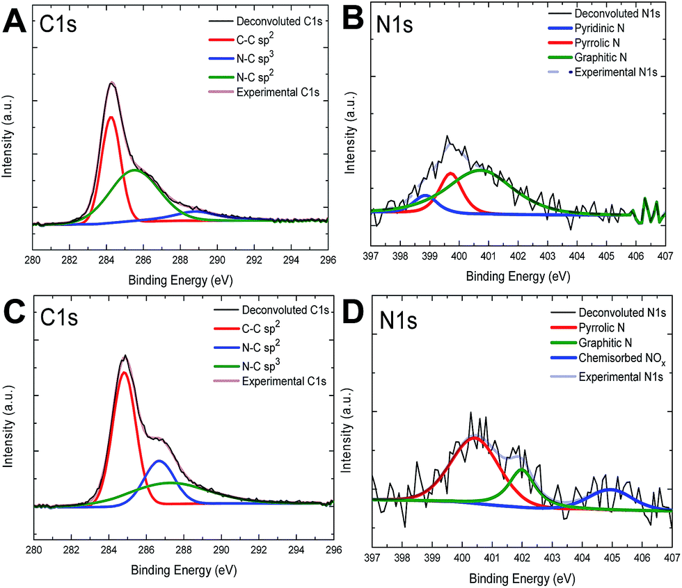 | ||
| Fig. 2 The XPS measurements of C 1s and N 1s band in N-graphene films on SiO2/Si treated by nitrogen plasma during (A and B) 15 min with RF-power of 10 W and (C and D) 20 min, with RF-power of 7 W, respectively. The nitrogen gas flow rate at plasma chamber was kept constant as 10 sccm. | ||
As reported in the literature,38 when RF-discharged with low power was used, the concentration of nitrogen increased with the treatment time. For instance, graphene treatment using an effective RF-power of 7 W and a plasma treatment time of 20 min provided a nitrogen concentration of 1.8 atomic%, while the treatment of graphene film using an RF-power of 10 W for 15 min led to 1.7 atomic% of nitrogen atoms in graphitic lattice. For the N-graphene treated by using an RF-power of 10 W for 15 min, the relative occurrences of the N-doping forms, namely, pyrrolic N, pyridinic N and graphitic N, were found as 0.3%, 0.2% and 1.2%, respectively. When the treatment conditions were changed to RF-power of 7 W for 20 min, the corresponding ratios for the N-doping forms of pyrrolic N, graphitic N and adsorbed (or chemisorbed) N, were found to be 1.1%, 0.4% and 0.3%, respectively. The N/C atomic ratio of samples was calculated by taking the ratio of the total area under the N 1s spectrum to that under the C 1s one. Also we found that the concentration of N atoms in graphitic lattice could be same with different plasma time and different types of nitrogen configurations.
3.3. Scanning tunneling microscopy and spectroscopy (STM and STS)
We also used STM to understand the local atomic structure in the vicinity of a N dopant in graphene sheets and sub-lattices. Spectroscopic analyses were utilized to measure the density of states and carrier concentration at nanoscale. The STM and STS measurements were performed over large areas of N-doped and pristine graphene samples for reference on Au (111) surface to investigate the configuration of nitrogen atoms.A representative large-area STM image of graphene is shown in Fig. 3A. As seen in Fig. 3B, the STM image of graphene showed honeycomb lattice indicating the fact that graphene layer on Au/mica was one layer. After nitrogen doping, STM images of N-graphene are shown in Fig. 3C–F. It was clearly seen that bombarded nitrogen atoms deformed the honeycomb structure and composed small clusters on graphitic lattice. Also the presence of some brighter sites in the selected region showed the doping of N atoms smoothly. The enlarged STM image of N-graphene (Fig. 3F) showed that nitrogen atoms have one unoccupied electron in valence band, were shaped in a triangular pattern on graphitic surface. As seen in Fig. 3F, these free electrons in C–N bonding cause an electron cloud around carbon atoms. This morphology changes due to the electronic configuration of nitrogen atom. We also investigated the electronic behaviour of pristine (red) and N-graphene (blue) via STS (Fig. 4). On the basis of the dI/dV characteristic, average energy gap for pristine graphene (Eg1) and N-graphene (Eg2) were measured as 205 meV and 317 meV, respectively. This was in good agreement with the calculated gap value. There is a gap in pristine graphene on Au (111). This gap may have occurred owing to the defect states in the honeycomb lattice, the weak graphene–Au (111) interaction or the intervalley scattering observed surrounding a point defect in the graphene layer on the Au (111) surface.65 After nitrogen doping, the difference in energy gap can be seen easily. Since the Dirac point of graphene on the Au (111) surface is located at EF,65 in STS data, there is no signature that could be associated with the presence of Dirac point in any particular position due to graphene–Au interaction as seen STS studies on graphene/Pt (111).66 This result may indicate that no appreciable doping of graphene exists for graphene/Au or no significant change expected in the energy position of the Dirac point. Fermi level is located in 0 meV as done in ref. 67–69. There are some peaks near Fermi level which are shown with asterisk in the dI/dV curve, it can be attributed to the presence of defect states. These states show that there is a change in electronic state of pristine graphene after plasma treatment.
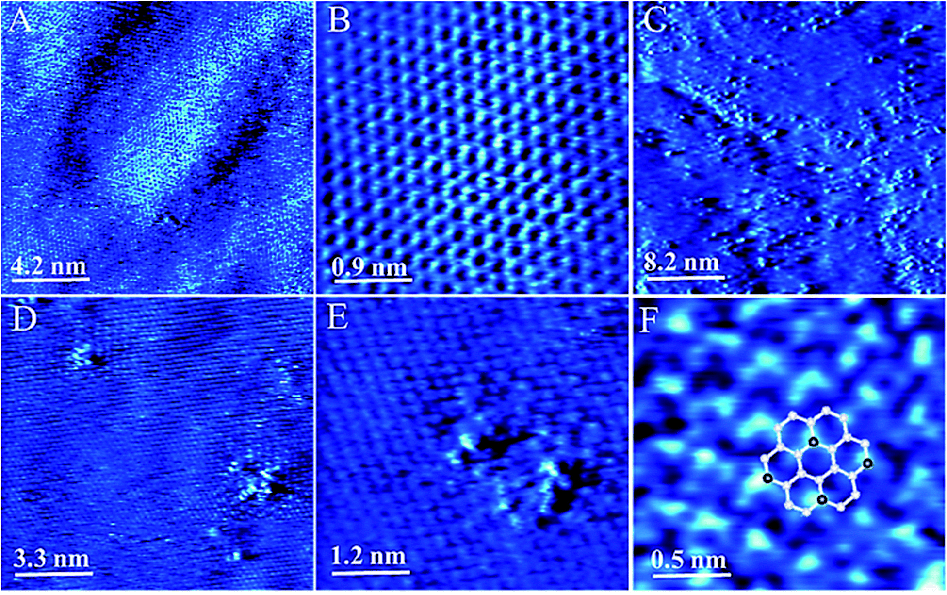 | ||
| Fig. 3 STM images of graphene (A and B) and N-graphene (C–F) on Au (111) substrate. In panel (F), simulated nitrogen and carbon atoms are shown as black and white dots, respectively. The STM images were recorded under constant-current mode with bias voltage varying between 25 and 70 mV and a 1 nA tunneling current. | ||
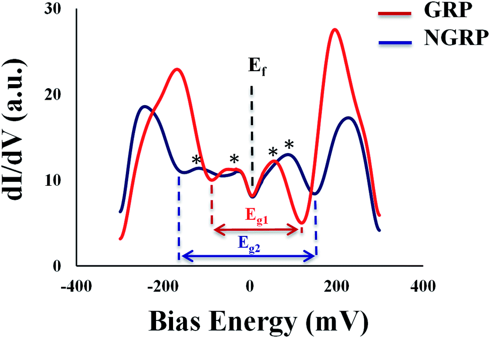 | ||
| Fig. 4 dI/dV characteristics of pristine (red line) and N-graphene (blue line) on Au (111). | ||
The experimental results show that the well-patterned regions formed by nitrogenation have a trigonal lattice periodicity that corresponds to a graphene supercell of  ×
×  × 1, containing one dopant atom. Moreover, another question is whether the doping occurs by adsorption of N atoms on the graphene host or by substitution of C atoms with N atoms. We infer about which option is more feasible for the atomic configuration of N dopants by comparing our DFT simulations with some measured properties of the N-graphene samples. For the substitutional case, the structural calculation shows that the substituted N is localized like a C atom in the lattice and the hexagonal symmetry is conserved as shown in Fig. 5A. The N–C bond length was found to be 1.40 Å which is slightly lower than the C–C bond length in bare graphene. Consequently, the lattice constant reduces from bare graphene lattice constant of 4.27 to 4.23 Å. In addition, Bader charge transfer analysis shows that C atoms donated 1.2e charged to N per atom. In the adsorption case, N prefers to localize over a C atom with a bond length of 1.46 Å as shown in Fig. 5D. The C atom slightly shifts towards the N atom which is charged by 0.4e. The C–C bonds in the vicinity of N slightly increases hence the lattice constant is extended to 4.32 Å.
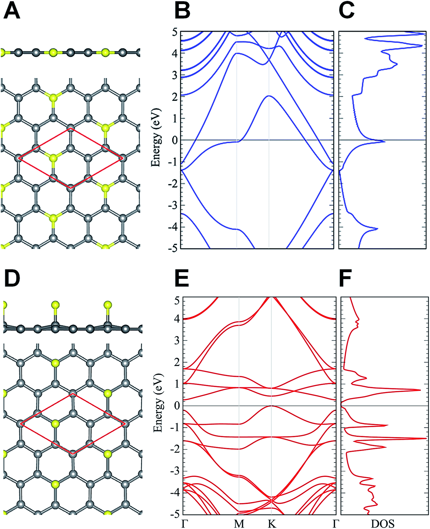 | ||
| Fig. 5 (A, D) The top and side views, (B, E) the energy band structure, and (C, F) density of states of N-substituted and N-adsorbed graphene, respectively. | ||
In addition, the electronic structure analysis reveals that substitution and adsorption of N results in different modifications in the electronic structure of graphene. In the substitution case, the system has metallic property. As shown in Fig. 5B and C the Fermi level of the well-known graphene like bands and DOS dispersions are shifted towards higher energies. This indicates that the graphene is n-type doped when the N doping is in the substitutional form. On the other hand, the adsorption of N opens an indirect band gap of 0.28 eV which is shown in Fig. 5E and F. The valance band maximum and conduction band minimum appears at K and Γ, respectively.
As the experimental band gap measurements indicate that the band gap of N-graphene increases compared to that of pristine graphene as shown in Fig. 3F. It was measured that graphene on Au (111) presented a semiconducting behaviour when doped with nitrogen. Experimental and theoretical results indicate that this further gap opening stems from adsorption of N atoms on the C atoms rather than substituting them in the lattice.
3.4. Fourier transform infrared spectroscopy (FTIR)
The FTIR spectroscopy measurements were performed to examine the changes in electronic and optical properties of pristine graphene and N-graphene. Fig. 6 presents the FTIR spectra of graphene before and after treatment. In the IR region of the spectrum, sapphire possesses high transmission at wavelengths ranging from 1.0 to 5.5 μm. In the 1.0 to 4.0 μm interval, the value of transmission is ∼85–86%.70 Sapphire background was not extracted from measurement result. Since the transmission of sapphire is dominant in the MIR region, sapphire as a substrate just decreases the total transmission of pristine and N-graphene. As reported in the literature,71 nitrogen containing ligands modify the graphene surface from hydrophobic to hydrophilic. As seen in Fig. 6, the peak at 3400 cm−1 may be attributed to the presence of oxygen-containing groups such as O–H groups being trapped on graphene after nitrogen plasma treatment. According to the transmission spectra, opening of the band gap was not observed however the decreased transmittance of N-graphene at 0.45 eV corresponded to absorption of N-graphene with the double energy of the shift of valence band maximum equivalent to 0.37 eV at 1.7 atomic% of nitrogen atoms. Furthermore our results were found to be in good agreement with literature.38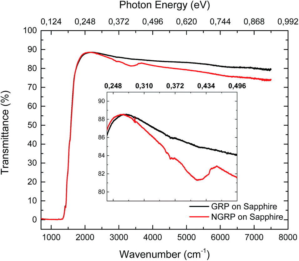 | ||
| Fig. 6 The transmission measurement of pristine graphene (GRP) and N-graphene (NGRP). Nitrogen doping parameters: nitrogen gas flow 10 sccm, effective RF-power 10 W, plasma time 15 min, nitrogen pressure 900 mTorr. | ||
4. Conclusions
In this paper we have presented an effective method for homogenously doping nitrogen into graphene using N2 plasma treatment and also theoretically elucidated whether the nitrogen doping is substitutional or by adsorption in character by means of DFT. Within this study, we successfully grew large area graphene with ethylene on copper foil at low pressure and low temperature by CVD method. The doping degree of N-doped graphene was controlled by plasma power and time under constant N2 flow rate. The most favorable doping parameters for homogeneity were determined. At these optimized parameters, 1.7 atomic% of nitrogen atoms were introduced to the graphitic lattice. According to XPS results, with increasing N2 plasma time and decreasing N2 plasma power, the pyridinic-N configuration disappeared and pyrollic-N became more dominant. The homogenous N-doping of graphene was further demonstrated via Raman spectroscopy, Scanning Tunneling Microscopy and Fourier Transform Infrared spectroscopy (FTIR). STS results showed an increase of nearly 100 meV in the band gap after doping the graphene on Au (111). The increment of the band gap is in good agreement with the theoretically demonstrated adsorption of nitrogens on the carbon lattice. Raman mapping of N-graphene on SiO2/Si clearly revealed homogeneity of nitrogen dopants in the graphitic lattice. To the best of our knowledge these results are new to the current literature and provide the opportunity to produce N-graphene with homogenous and effective doping which would be valuable for various applications.Acknowledgements
The authors acknowledge AQuReC facilities at IZTECH for XPS and Raman measurements, and TUBITAK for financial support (Project number 112T946). This article is dedicated to the memory of Prof. Yusuf Selamet.References
- A. K. Geim and K. S. Novoselov, Nat. Mater., 2007, 6, 183–191 CrossRef CAS PubMed.
- K. Novoselov, D. Jiang, F. Schedin, T. Booth, V. Khotkevich, S. Morozov and A. Geim, Proc. Natl. Acad. Sci. U. S. A., 2005, 102, 10451–10453 CrossRef CAS PubMed.
- X. Wang, X. Li, L. Zhang, Y. Yoon, P. K. Weber, H. Wang, J. Guo and H. Dai, Science, 2009, 324, 768–771 CrossRef CAS PubMed.
- X. Wang, Y. Ouyang, X. Li, H. Wang, J. Guo and H. Dai, Phys. Rev. Lett., 2008, 100, 206803 CrossRef PubMed.
- A. C. Neto, F. Guinea, N. M. Peres, K. S. Novoselov and A. K. Geim, Rev. Mod. Phys., 2009, 81, 109 CrossRef.
- N. Peres, Rev. Mod. Phys., 2010, 82, 2673 CrossRef CAS.
- F. Tikhonenko, A. Kozikov, A. Savchenko and R. Gorbachev, Phys. Rev. Lett., 2009, 103, 226801 CrossRef CAS PubMed.
- J. Zhang, J. Li, Z. Wang, X. Wang, W. Feng, W. Zheng, W. Cao and P. Hu, Chem. Mater., 2014, 26, 2460–2466 CrossRef CAS.
- H. L. Poh, P. Šimek, Z. k. Sofer and M. Pumera, ACS Nano, 2013, 7, 5262–5272 CrossRef CAS PubMed.
- L. Panchakarla, K. Subrahmanyam, S. Saha, A. Govindaraj, H. Krishnamurthy, U. Waghmare and C. Rao, arXiv preprint arXiv:0902.3077, 2009.
- M. Deifallah, P. F. McMillan and F. Corà, J. Phys. Chem. C, 2008, 112, 5447–5453 CAS.
- Y.-C. Lin, C.-Y. Lin and P.-W. Chiu, Appl. Phys. Lett., 2010, 96, 133110 CrossRef.
- A. L. M. Reddy, A. Srivastava, S. R. Gowda, H. Gullapalli, M. Dubey and P. M. Ajayan, ACS Nano, 2010, 4, 6337–6342 CrossRef CAS PubMed.
- H. Wang, C. Zhang, Z. Liu, L. Wang, P. Han, H. Xu, K. Zhang, S. Dong, J. Yao and G. Cui, J. Mater. Chem., 2011, 21, 5430–5434 RSC.
- Y. Wang, Y. Shao, D. W. Matson, J. Li and Y. Lin, ACS Nano, 2010, 4, 1790–1798 CrossRef CAS PubMed.
- C. Zhang, L. Fu, N. Liu, M. Liu, Y. Wang and Z. Liu, Adv. Mater., 2011, 23, 1020–1024 CrossRef CAS PubMed.
- H. M. Jeong, J. W. Lee, W. H. Shin, Y. J. Choi, H. J. Shin, J. K. Kang and J. W. Choi, Nano Lett., 2011, 11, 2472–2477 CrossRef CAS PubMed.
- J. F. Bao, N. Kishi and T. Soga, Mater. Lett., 2014, 117, 199–203 CrossRef CAS.
- H. Wang, T. Maiyalagan and X. Wang, ACS Catal., 2012, 2, 781–794 CrossRef CAS.
- S. H. Park, J. Chae, M.-H. Cho, J. H. Kim, K.-H. Yoo, S. W. Cho, T. G. Kim and J. W. Kim, J. Mater. Chem. C, 2014, 2, 933–939 RSC.
- L. Qu, Y. Liu, J.-B. Baek and L. Dai, ACS Nano, 2010, 4, 1321–1326 CrossRef CAS PubMed.
- R. I. Jafri, N. Rajalakshmi and S. Ramaprabhu, J. Mater. Chem., 2010, 20, 7114–7117 RSC.
- D. Wei, Y. Liu, Y. Wang, H. Zhang, L. Huang and G. Yu, Nano Lett., 2009, 9, 1752–1758 CrossRef CAS PubMed.
- H. Gao, L. Song, W. Guo, L. Huang, D. Yang, F. Wang, Y. Zuo, X. Fan, Z. Liu and W. Gao, Carbon, 2012, 50, 4476–4482 CrossRef CAS.
- T. Schiros, D. Nordlund, L. Paálovaá, D. Prezzi, L. Zhao, K. S. Kim, U. Wurstbauer, C. Gutieérrez, D. Delongchamp and C. Jaye, Nano Lett., 2012, 12, 4025–4031 CrossRef CAS PubMed.
- Y.-F. Lu, S.-T. Lo, J.-C. Lin, W. Zhang, J.-Y. Lu, F.-H. Liu, C.-M. Tseng, Y.-H. Lee, C.-T. Liang and L.-J. Li, ACS Nano, 2013, 7, 6522–6532 CrossRef CAS PubMed.
- T. Wu, H. Shen, L. Sun, B. Cheng, B. Liu and J. Shen, New J. Chem., 2012, 36, 1385–1391 RSC.
- P. Lambin, H. Amara, F. Ducastelle and L. Henrard, Phys. Rev. B: Condens. Matter Mater. Phys., 2012, 86, 045448 CrossRef.
- Z. Jin, J. Yao, C. Kittrell and J. M. Tour, ACS Nano, 2011, 5, 4112–4117 CrossRef CAS PubMed.
- C. Wang, M. F. Yuen, T. W. Ng, S. K. Jha, Z. Lu, S. Y. Kwok, T. L. Wong, X. Yang, C. S. Lee and S. T. Lee, Appl. Phys. Lett., 2012, 100, 253107 CrossRef.
- Z. Luo, S. Lim, Z. Tian, J. Shang, L. Lai, B. MacDonald, C. Fu, Z. Shen, T. Yu and J. Lin, J. Mater. Chem., 2011, 21, 8038–8044 RSC.
- D. Geng, Y. Chen, Y. Chen, Y. Li, R. Li, X. Sun, S. Ye and S. Knights, Energy Environ. Sci., 2011, 4, 760–764 CAS.
- X. Li, H. Wang, J. T. Robinson, H. Sanchez, G. Diankov and H. Dai, J. Am. Chem. Soc., 2009, 131, 15939–15944 CrossRef CAS PubMed.
- Y. Shao, S. Zhang, M. H. Engelhard, G. Li, G. Shao, Y. Wang, J. Liu, I. A. Aksay and Y. Lin, J. Mater. Chem., 2010, 20, 7491–7496 RSC.
- K. Kinoshita, Carbon: electrochemical and physicochemical properties, John Wiley & Sons, New York, 1988 Search PubMed.
- H. C. Lee, W.-W. Liu, S.-P. Chai, A. R. Mohamed, C. W. Lai, C.-S. Khe, C. Voon, U. Hashim and N. Hidayah, Procedia Chem., 2016, 19, 916–921 CrossRef CAS.
- J. K. Wassei, M. Mecklenburg, J. A. Torres, J. D. Fowler, B. Regan, R. B. Kaner and B. H. Weiller, Small, 2012, 8, 1415–1422 CrossRef CAS PubMed.
- M. Rybin, A. Pereyaslavtsev, T. Vasilieva, V. Myasnikov, I. Sokolov, A. Pavlova, E. Obraztsova, A. Khomich, V. Ralchenko and E. Obraztsova, Carbon, 2016, 96, 196–202 CrossRef CAS.
- L. Zhao, R. He, K. T. Rim, T. Schiros, K. S. Kim, H. Zhou, C. Gutiérrez, S. Chockalingam, C. J. Arguello and L. Pálová, Science, 2011, 333, 999–1003 CrossRef CAS PubMed.
- R. Podila, J. Chacón-Torres, J. Spear, T. Pichler, P. Ayala and A. M. Rao, Appl. Phys. Lett., 2012, 101, 123108 CrossRef.
- C. Mattevi, H. Kim and M. Chhowalla, J. Mater. Chem., 2011, 21, 3324–3334 RSC.
- F. Joucken, Y. Tison, J. Lagoute, J. Dumont, D. Cabosart, B. Zheng, V. Repain, C. Chacon, Y. Girard and A. R. Botello-Méndez, Phys. Rev. B: Condens. Matter Mater. Phys., 2012, 85, 161408 CrossRef.
- A. Tomak, C. Bacaksiz, G. Mendirek, H. Sahin, D. Hur, K. Görgün, R. Senger, Ö. Birer, F. Peeters and H. Zareie, Nanotechnology, 2016, 27, 335601 CrossRef CAS PubMed.
- J. P. Perdew, K. Burke and M. Ernzerhof, Phys. Rev. Lett., 1996, 77, 3865 CrossRef CAS PubMed.
- J. P. Perdew, K. Burke and M. Ernzerhof, Phys. Rev. Lett., 1997, 78, 1396 CrossRef CAS.
- G. Kresse and J. Hafner, Phys. Rev. B: Condens. Matter Mater. Phys., 1993, 48, 13115 CrossRef CAS.
- G. Kresse and J. Hafner, Phys. Rev. B: Condens. Matter Mater. Phys., 1994, 49, 14251 CrossRef CAS.
- S. Grimme, J. Comput. Chem., 2006, 27, 1787–1799 CrossRef CAS PubMed.
- G. Henkelman, A. Arnaldsson and H. Jónsson, Comput. Mater. Sci., 2006, 36, 354–360 CrossRef.
- Z. Zafar, Z. H. Ni, X. Wu, Z. X. Shi, H. Y. Nan, J. Bai and L. T. Sun, Carbon, 2013, 61, 57–62 CrossRef CAS.
- M. Pimenta, G. Dresselhaus, M. S. Dresselhaus, L. Cancado, A. Jorio and R. Saito, Phys. Chem. Chem. Phys., 2007, 9, 1276–1290 RSC.
- R. Beams, L. G. Cançado and L. Novotny, J. Phys.: Condens. Matter, 2015, 27, 083002 CrossRef PubMed.
- D. Graf, F. Molitor, K. Ensslin, C. Stampfer, A. Jungen, C. Hierold and L. Wirtz, Eur. Phys. J.: Spec. Top., 2007, 148, 171–176 CrossRef.
- A. Tiberj, J.-R. Huntzinger, J. Camassel, F. Hiebel, A. Mahmood, P. Mallet, C. Naud and J.-Y. Veuillen, Nanoscale Res. Lett., 2011, 6, 1–8 Search PubMed.
- T. Yu, Z. Ni, C. Du, Y. You, Y. Wang and Z. Shen, J. Phys. Chem. C, 2008, 112, 12602–12605 CAS.
- R. Lv, Q. Li, A. R. Botello-Méndez, T. Hayashi, B. Wang, A. Berkdemir, Q. Hao, A. L. Elías, R. Cruz-Silva and H. R. Gutiérrez, Sci. Rep., 2012, 2(586), 1–8 Search PubMed.
- H.-K. Seo, T.-S. Kim, C. Park, W. Xu, K. Baek, S.-H. Bae, J.-H. Ahn, K. Kim, H. C. Choi and T.-W. Lee, Sci. Rep., 2015, 5(16710), 1–10 Search PubMed.
- T. Tsukamoto, K. Yamazaki, H. Komurasaki and T. Ogino, J. Phys. Chem. C, 2012, 116, 4732–4737 CAS.
- Y. Y. Wang, Z. H. Ni, T. Yu, Z. X. Shen, H. M. Wang, Y. H. Wu, W. Chen and A. T. Shen Wee, J. Phys. Chem. C, 2008, 112, 10637–10640 CAS.
- H. Liu, Y. Zhang, R. Li, X. Sun, S. Désilets, H. Abou-Rachid, M. Jaidann and L.-S. Lussier, Carbon, 2010, 48, 1498–1507 CrossRef CAS.
- H. Xiang, B. Huang, Z. Li, S.-H. Wei, J. Yang and X. Gong, Phys. Rev. X, 2012, 2, 011003 Search PubMed.
- X. Du, H.-Y. Liu and Y.-W. Mai, ACS Nano, 2015, 10, 453–462 CrossRef PubMed.
- X. Du, C. Zhou, H.-Y. Liu, Y.-W. Mai and G. Wang, J. Power Sources, 2013, 241, 460–466 CrossRef CAS.
- R. Zhao, T. Afaneh, R. Dharmasena, J. Jasinski, G. Sumanasekera and V. Henner, Phys. B, 2016, 490, 21–24 CrossRef CAS.
- L. Gao, Graphene and 2D Materials, 2014, 1, 23–46 CrossRef.
- J. Sławińska and I. Zasada, Phys. Rev. B: Condens. Matter Mater. Phys., 2011, 84, 235445 CrossRef.
- S. Jung, G. M. Rutter, N. N. Klimov, D. B. Newell, I. Calizo, A. R. Hight-Walker, N. B. Zhitenev and J. A. Stroscio, Nat. Phys., 2011, 7, 245–251 CrossRef CAS.
- P. Nirmalraj, D. Thompson, A. Molina-Ontoria, M. Sousa, N. Martín, B. Gotsmann and H. Riel, Nat. Mater., 2014, 13, 947–953 CrossRef CAS PubMed.
- S. Barja, S. Wickenburg, Z.-F. Liu, Y. Zhang, H. Ryu, M. M. Ugeda, Z. Hussain, Z.-X. Shen, S.-K. Mo and E. Wong, Nat. Phys., 2016, 12, 751–756 CrossRef CAS.
- E. R. Dobrovinskaya, L. A. Lytvynov and V. Pishchik, Sapphire: material, manufacturing, applications, Springer Science & Business Media, 2009 Search PubMed.
- A. Dey, A. Chroneos, N. S. J. Braithwaite, R. P. Gandhiraman and S. Krishnamurthy, Appl. Phys. Rev., 2016, 3, 021301 Search PubMed.
| This journal is © The Royal Society of Chemistry 2017 |