
 Open Access Article
 This Open Access Article is licensed under a Creative Commons Attribution-Non Commercial 3.0 Unported Licence
Fabrication of periodic arrays of needle-like Si nanowires on (001)Si and their enhanced field emission characteristics
S. L. Cheng *ab,
H. C. Lina,
Y. H. Huanga and
S. C. Yanga
*ab,
H. C. Lina,
Y. H. Huanga and
S. C. Yanga
aDepartment of Chemical and Materials Engineering, National Central University, Chung-Li District, Taoyuan City, Taiwan, Republic of China. E-mail: slcheng@ncu.edu.tw; Tel: +886-3-4227151ext. 34233
bInstitute of Materials Science and Engineering, National Central University, Chung-Li District, Taoyuan City, Taiwan, Republic of China
First published on 3rd May 2017
Abstract
Well-ordered arrays of needle-like and cone-like Si nanostructures have been successfully produced on (001)Si substrates. The morphology and dimensions of the tapered Si nanostructure arrays can be readily controlled by adjusting the Ag-nanoparticle catalytic etching/removal (ACER) cycles. All the produced vertical tapered Si nanostructures were single crystalline and their axial crystallographic orientation was the same as that of the (001)Si substrate. The produced long needle-like Si nanowires exhibited superior field emission properties compared to as-produced and short cone-like Si nanowires. The enhanced field emission performance of the long needle-like Si nanowire array can be attributed to the good vertical alignment, sharp tips, high aspect ratio, single-crystalline structure, and well-ordered arrangement. The experimental results present the exciting prospect that with appropriate control, the combined approach proposed here promises to be applicable for fabricating other highly-ordered, vertically-aligned tapered Si-based nanowire arrays and may offer potential applications in constructing various high efficiency Si-based field emission nanodevices.
1. Introduction
In recent years, low dimensional nanostructures, in particular one-dimensional (1D) Si-based nanostructures, such as nanowires, nanocones, and nanotubes, have attracted a lot of attention because of their unique physical characteristics. Among these physical properties, electron field emission is one of the properties of great commercial interest in flat panel displays and vacuum microelectronics.1,2 The high aspect ratio, good mechanical strength and compatibility with conventional IC fabrication processes make 1D Si-based nanostructures the most promising emitters for field emission devices. A variety of fabrication methods, including laser ablation,3 chemical vapor deposition (CVD),4,5 RIE-based dry etching,6,7 and metal-catalytic chemical etching,8–10 have been developed to fabricate large-scale Si nanowires and/or pyramids (cones) which were used in field emitter arrays. However, it is found that a relatively high electrical field is usually required to initiate field emission from these produced Si nanostructures. This is due to the low aspect ratio of pyramidal Si nanocones and the random crystallographic orientations, dimensions, and locations of Si nanowires that are formed by the above-described methods. To overcome these drawbacks, an effective and economical method which is based on the oxygen plasma modified nanosphere lithography and Au-assisted catalytic etching process has recently been proposed.11–13 Although this nanosphere-templated etching approach has been successfully applied to produce well-ordered arrays of vertically-aligned Si nanowires with uniform diameters on various types of Si substrates, the top-ends of the produced Si nanowires are usually blunt and flat.14–17 It should be noted that previous studies have demonstrated that the field emission performance of nanowires can be further enhanced through sharpening the tips of nanowires.18,19Lv et al. presented a dry oxidation process to reduce the tip diameter of vertical Si nanowires.20 Their study showed that by using this method, the vertical Si nanowires with tapered tips were successfully produced on Si substrates and the tip diameter could be reduced from 480 nm to 180 nm. However, the main drawback of this approach is that it requires high operating temperature (∼1050 °C) and sufficient long annealing time (∼1 h). To fabricate tapered Si nanowire arrays at low temperature and short reaction time, Hsu et al. developed a wet etching process, which was performed by immersing the Si nanowires in a KOH aqueous solution for a few seconds.21 Although the diameter of Si nanowires could be reduced down to several tens of nanometers by using the KOH-etching method, the top-end morphology of the KOH-etched Si nanowires was found to be non-uniform. Recently, another room-temperature multiple catalytic etching/removal cycle process was developed by Lin et al.22, in which the top ends of vertical Si nanopillars could be uniformly reduced. Therefore, in this study, we propose taking advantage of the oxygen plasma modified nanosphere lithography in conjunction with the Au-assisted catalytic etching process to fabricate size-controllable, periodic arrays of vertically-aligned Si nanowires on (001)Si substrates. Subsequently, the tips of the produced vertical Si nanowires are carefully sharpened by means of multiple catalytic etching/removal cycle process at room temperature. The results from a systematic investigation of the morphological and structural evolution, crystallographic orientation, surface wetting behaviors, and electron field emission characteristics of vertical needle-like Si nanowire arrays produced under different wet catalytic etching conditions are reported.
2. Experimental
Single crystal, boron-doped (001) oriented Si wafers with resistivities of 1–10 Ω cm were cut into pieces of about 10 × 10 mm2 and used as the starting materials in this study. Fig. 1 shows the schematic illustration of the fabrication procedures of vertically-aligned Si nanowire arrays with tapered tips. Monodispersed polystyrene (PS) nanospheres with a mean diameter of 400 nm were utilized to form a hexagonal close-packed PS nanosphere monolayer on HF-dipped (001)Si substrate according to the procedures described elsewhere.23 The diameter of the self-assembled PS nanospheres was then trimmed to desirable levels by O2 plasma treatments at a pressure of 0.3 mbar and a power of 60 W. Subsequently, a 20 nm-thick catalytic Au thin film was deposited onto the nonclose-packed PS nanosphere array patterned (001)Si substrates by electron beam evaporation at room temperature in a vacuum better than 4 × 10⁻⁶ Torr. The Au-assisted catalytic etching process was conducted in a mixed etching solution of H2O2, HF, and H2O at 20 °C to form vertically-aligned Si nanowires with a length of 2 μm. Once the vertical Si nanowires formed on (001)Si substrates, the catalytic Au films and nonclose-packed PS nanosphere templates were removed by dissolving in an aqua regia solution and in a tetrahydrofuran (THF) solution, respectively. In order to further modulate the top-end morphology of the produced Si nanowires, a multiple Ag-nanoparticle catalytic etching/removal (ACER) cycle process was adopted. In each cycle, the Ag-nanoparticle catalytic etching process was performed by immersing the Si nanowires in a solution mixture of AgNO3, HNO3, HF, and H2O at room temperature for 2 min, and then the catalytic Ag nanoparticles wrapping the surfaces of the Si nanowires were removed by rinsing in a dilute HNO3 aqueous solution. | ||
| Fig. 1 Schematic diagram illustrating the experimental procedures for the fabrication of vertically-aligned periodic arrays of tapered Si nanowires and Si nanocones on (001)Si substrates. | ||
A scanning electron microscope (SEM, Hitachi S-3000H) was utilized to examine the sizes, lengths, and surface morphologies of the self-assembled PS nanosphere array templates and the vertical Si nanowire arrays produced at various numbers of etching cycles. The microstructures examination and crystallographic orientations determination were carried out using a transmission electron microscope (TEM, JEOL JEM2000FXII), a high-resolution TEM (HRTEM, JEOL JEM2100), and the selected-area electron diffraction (SAED) technique. The surface wetting properties of the various Si nanowire samples were characterized by water contact angle (CA) measurements. The volume of each water droplet was fixed at 4 μL. The electron field emission measurement was carried out in a custom-built high vacuum system at room temperature. The base pressure in the chamber was better than 1 × 10⁻⁶ Torr. A stainless-steel cuboid was used as the anode, and the gap between the anode and the surface of Si nanowires (cathode) was fixed at 80 μm during measurements. Prior to the water contact angle and field emission measurements, all of the vertical Si nanowire arrays with different tip morphologies were dipped in a dilute HF solution to remove the native oxide layer.
3. Results and discussion
Fig. 2(a) and its inset show, respectively, the top-view SEM images of the self-assembled close-packed monolayer array of 400 nm-diameter PS nanospheres on the surface of Si substrate before and after O2 plasma treatments. It is clearly seen from Fig. 2(a) that the diameter of PS nanospheres was reduced uniformly from 400 nm to 120 nm by appropriate O2 plasma treatments. Using the hexagonally-ordered nonclose-packed PS nanosphere array as the etching template, a periodic array of 2 μm-length Si nanowires was successfully fabricated on (001)Si substrate via the Au-assisted catalytic etching process. Examples are shown in Fig. 2(b) and (c). As can be seen in these SEM images, the produced Si nanowires, after removal of the catalytic Au film and PS nanospheres, were vertically aligned and had the same diameter and hexagonal periodicity as that of the O2 plasma-trimmed PS nanosphere template used in this study. The inset of Fig. 2(c) shows a representative photograph of a water droplet on the surface of the produced Si nanowire sample after dipping the sample in a dilute HF solution. The water contact angle measurement revealed that the HF-dipped Si nanowire array exhibited strong hydrophobicity with a water contact angle of 139°. The observed hydrophobic behavior could be explained by the Cassie–Baxter model.24 The morphology and crystal structure of Si nanowires were investigated in detail by TEM and SAED analysis. It is evident from the representative TEM image shown in Fig. 2(d) that as-produced Si nanowires have relatively smooth and clean surfaces and flat top-ends. From the analysis of the corresponding SAED pattern, as shown in the inset of Fig. 2(d), all the as-produced Si nanowires were found to have a single-crystalline nature and their axial orientations were identified to be parallel to the [001] direction, which was identical to the crystallographic orientation of the (001)Si substrate used.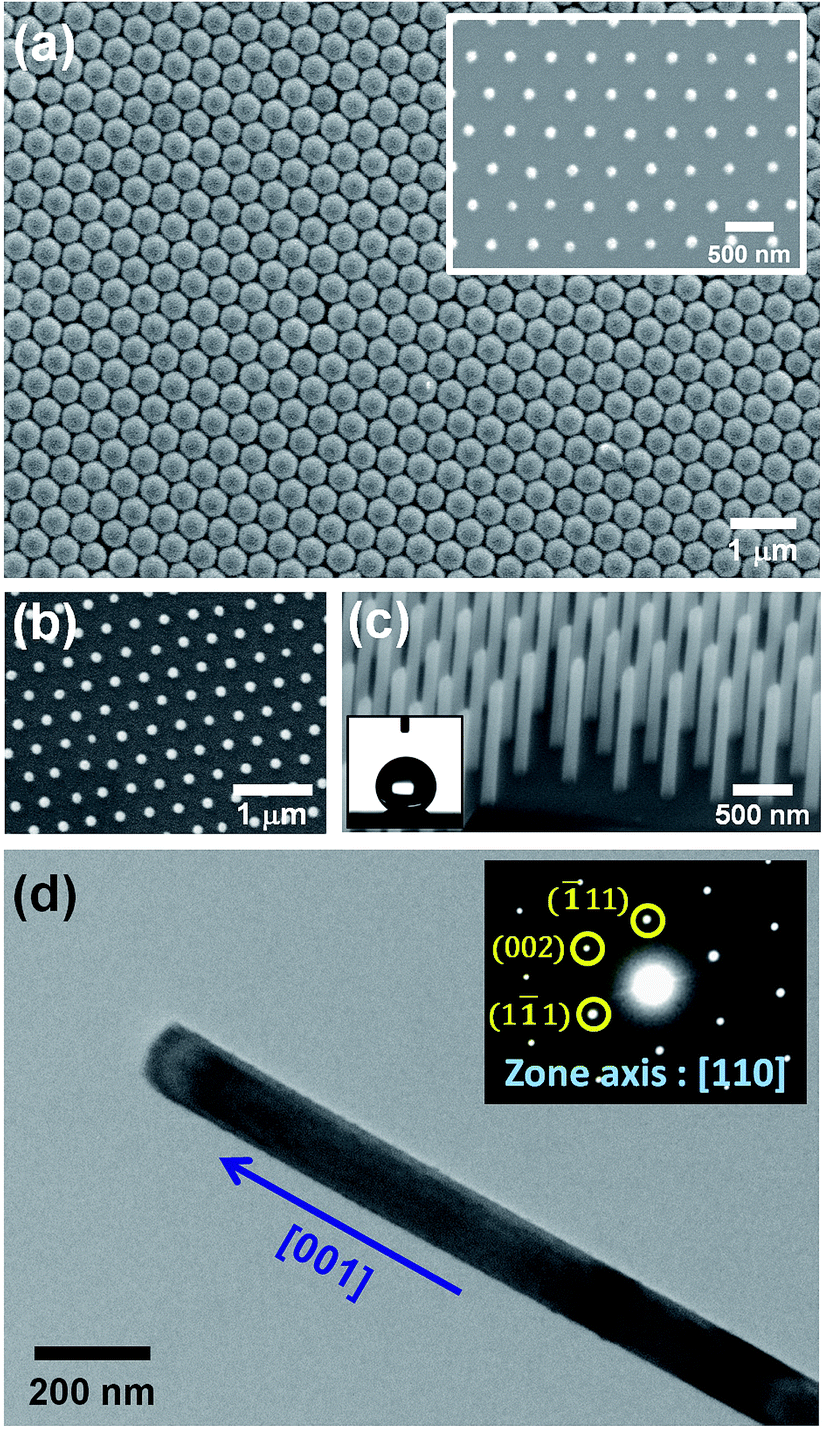 | ||
| Fig. 2 (a) A top-view SEM image of a self-assembled monolayer of 400 nm-diameter PS nanospheres on (001)Si substrate. The inset is the corresponding high-magnification SEM image of the PS nanosphere template after O2 plasma treatment. (b) Top-view and (c) tilted-view SEM images of as-produced vertical Si nanowire arrays on (001)Si substrate. The inset in (c) is a representative photograph of a water droplet on the surface of HF-dipped Si nanowires. (d) A representative TEM image of an as-produced Si nanowire. The inset is the corresponding indexed SAED pattern. | ||
Following the Si nanowires formation process, a multiple ACER cycle process was used to further sharpen the top-ends of the vertically-aligned Si nanowires. Fig. 3(a) shows a representative TEM image of as-produced Si nanowires treated in a mixed etching solution of AgNO3, HNO3, HF, and H2O for 2 min, from which it can be seen that there are many nanoparticles on the top and side surfaces of Si nanowires and the nanoparticle sizes gradually decrease along the axial direction of Si nanowires. From SAED analysis, as shown in Fig. 3(b), diffraction rings corresponding to the FCC structure of Ag phase were detected in the SAED pattern, indicating that the deposited nanoparticles were pure Ag nanoparticles. After etching the Ag nanoparticles away, numerous vertical and lateral etched nanoholes or nanochannels were clearly seen. An example is shown in Fig. 3(c). The detailed mechanism of the vertical and lateral etching of Si catalyzed by Ag nanoparticles has been reported in several previous studies.25–27 Fig. 4(a)–(f) are the representative SEM images showing the morphological evolution of the Si nanowires with the number of the ACER cycles. As can be seen from these SEM images, after repeating the ACER cycle up to four times, a periodic array of vertical Si nanowires with needle-like tips could be successfully fabricated. Furthermore, the SEM examinations also revealed that with increasing the number of the ACER cycles, the morphology of the etched Si nanowires gradually changed from a needle-like shape to a cone-like one with a shorter length. The corresponding plot of the average length of Si nanowires as a function of the number of the ACER cycles is shown in Fig. 4(g). The observed results clearly demonstrate that the morphology and dimension of Si nanowires could be readily controlled by adjusting the Ag-nanoparticle catalytic etching conditions. In order to investigate the tip dimension and morphology, and the atomic crystal structure of the vertical Si nanowires after multiple ACER cycles in more detail, TEM and HRTEM analyses were carried out.
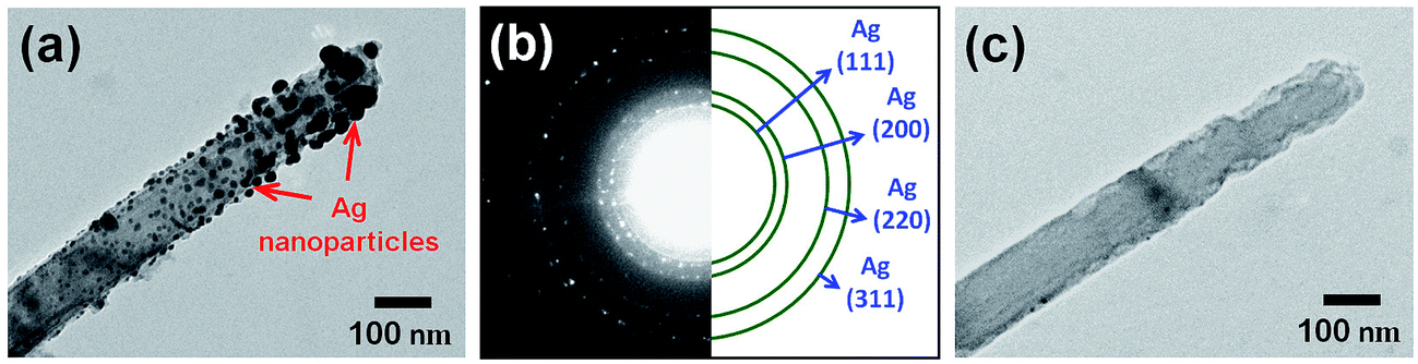 | ||
| Fig. 3 (a) A representative TEM image and (b) the corresponding indexed SAED pattern of an as-produced Si nanowire after the Ag-nanoparticle catalytic etching for 2 min. (c) The corresponding TEM image of an etched Si nanowire after removal of Ag nanoparticle catalysts. | ||
 | ||
| Fig. 4 Tilted-view SEM images of vertical Si nanowire arrays after the (a) 2nd, (b) 4th, (c) 6th, (d) 8th, (e) 11th, and (f) 14th ACER cycle. (g) A plot of the average length of Si nanowires versus the number of the ACER cycles. | ||
The TEM images, as shown in Fig. 5(a)–(c), clearly revealed that long needle-like and short cone-like Si nanowires were produced after the 4th (or 6th) and 11th ACER cycle, respectively. The tips of both needle-like and cone-like Si nanowires were very sharp. However, with closer examinations, the surfaces of upper parts of these etched Si nanowires were slightly rough. The formation of etched pits and cavities on the surfaces could be attributed to the Ag-nanoparticle catalytic etching process. Fig. 5(d) and (e) show, respectively, the corresponding HRTEM images, taken along the [110] zone axis, from the tip regions of Si nanowires after the 4th and 11th ACER cycle. It is clear that the atoms are arranged in a regular sequence, and the measured atomic lattice spacings of 0.272 and 0.314 nm are in good agreement with the interplanar distances of the {002} and {1![[1 with combining macron]](https://www.rsc.org/images/entities/char_0031_0304.gif) 1} lattice planes of a pure Si crystal, respectively. The results of HRTEM and SAED (the insets of Fig. 5(a) and (c)) analyses confirmed that the etched Si nanowires still remained single crystalline with an axial orientation along the [001] direction even after the 11th ACER cycle. Furthermore, the tip diameters of the produced tapered Si nanowires and Si nanocones were all found to be less than 10 nm.
1} lattice planes of a pure Si crystal, respectively. The results of HRTEM and SAED (the insets of Fig. 5(a) and (c)) analyses confirmed that the etched Si nanowires still remained single crystalline with an axial orientation along the [001] direction even after the 11th ACER cycle. Furthermore, the tip diameters of the produced tapered Si nanowires and Si nanocones were all found to be less than 10 nm.
 | ||
| Fig. 5 Representative TEM images of Si nanowires after the (a) 4th, (b) 6th, and (c) 11th ACER cycle. The insets are the corresponding indexed SAED pattern. Representative HRTEM images from the tip regions of Si nanowires after the (d) 4th and (e) 11th ACER cycle. | ||
It is known that surface morphology and roughness would significantly affect the wettability of a solid substrate with water. In the case of a hydrophobic surface, surface roughness can enhance hydrophobicity.28,29 Thus, it is of both fundamental and scientific interests to evaluate the surface wettability of Si nanowire samples after different number of the ACER cycles. Fig. 6 shows the variation of water contact angles of HF-dipped Si nanowire samples as a function of the number of the ACER cycles. For comparison, the water contact angle of the HF-treated blank-(001)Si substrate with a smooth surface was also measured and found to be about 85°. As can be seen in Fig. 6, the water contact angle values gradually decreased from initial 139° to about 89°, indicating that the surface hydrophobicity of Si nanowire samples gradually declined with increasing the cycle number. The observed changes in surface wettability can be explained by the Cassie–Baxter model.24 According to this model, air is trapped in nanostructures underneath the water droplet. The presence of a large amount of air pockets on the submerged surface enhances the hydrophobicity of the nanostructure surface. In this study, it is found from the SEM results (Fig. 4) that with increasing the number of the ACER cycles, the vertical Si nanowires gradually changed from a long needle-like shape to a short cone-like one. When a water droplet is placed on the surface of hydrophobic Si nanowires, it can be expected that the amount of air trapped in the interstices below the water droplet decreases as the length of Si nanowires decreases. A smaller amount of air trapped in the interstices of hydrophobic Si nanowires would therefore reduce the surface hydrophobicity of Si nanowire samples.
 | ||
| Fig. 6 Variation of water contact angles of the etched Si nanowire samples with the number of the ACER cycles. The insets are the corresponding photographs of water droplets on the sample surfaces. | ||
Based on the above experimental results, the formation mechanism of well-ordered arrays of vertically-aligned tapered Si nanostructures fabricated by the multiple ACER cycles are summarized; see the schematic illustration in Fig. 7. First, due to the hydrophobic nature of HF-dipped Si nanowire surfaces, the electroless deposition of catalytic Ag nanoparticles occurred only on the upper part (top and side surfaces) of the Si nanowires (Fig. 7(a)). Each Ag nanoparticle acted as a catalyst that initiated the Ag-catalyzed etching process. Subsequently, oxidation and dissolution of Si atoms occurred at the interface of Ag nanoparticle and Si nanowire, leading to vertical and lateral anisotropic etching of the Si nanowire surfaces (Fig. 7(b)). After HNO3 removal of Ag nanoparticles, truncated Si nanowires with reduced tip diameters were formed (Fig. 7(c)). Through repeated the Ag-nanoparticle catalytic etching/removal cycle, the upper part of the Si nanowires continued to be etched and gradually became sharper (Fig. 7(d)–(f)). After multiple Ag-nanoparticle catalytic etching/removal cycles, long needle-like and/or short cone-like Si nanostructure arrays could then be obtained (Fig. 7(g) and (h)).
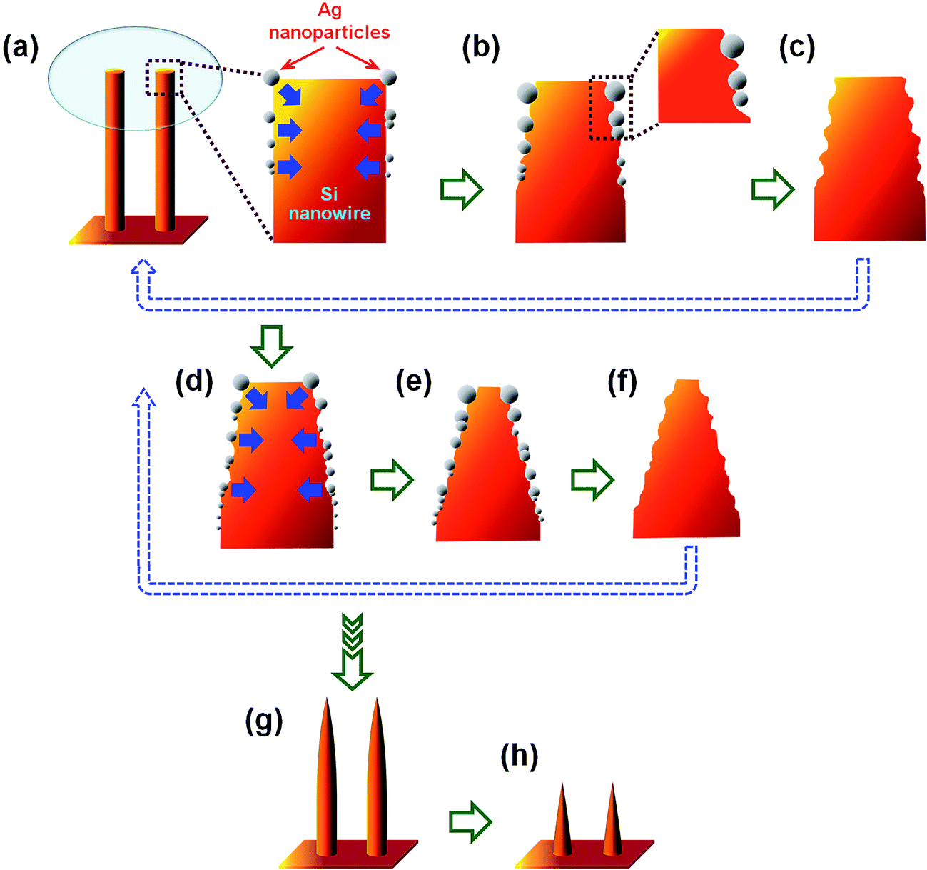 | ||
| Fig. 7 Schematic illustration of the formation mechanism with morphological evolution of vertically-aligned tapered Si nanostructure arrays fabricated by multiple ACER cycles. | ||
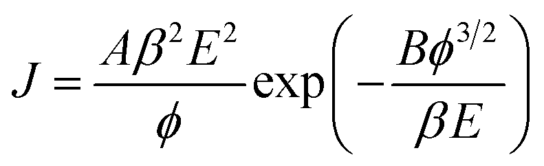
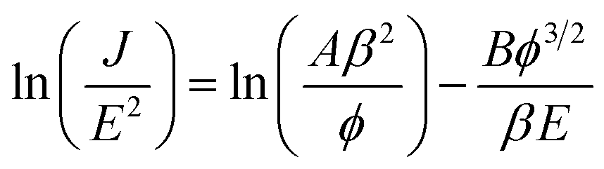
In order to evaluate the electron field emission characteristics of the different types of tapered Si nanostructure arrays produced in this study, a series of measurements were performed and compared. Fig. 8(a) shows the field emission current density (J) as a function of the applied electric field (E) for the vertical Si nanowire arrays before and after the 4th, 6th, and 11th ACER cycle. The turn-on fields (defined as the applied electric field required to produce a emission current density of 10 μA cm−2) for the Si nanowire arrays after the 4th, 6th, and 11th ACER cycle were measured to be about 1.3, 1.5, and 3.8 V μm−1, respectively, which were much lower than that for as-produced Si nanowires with flat top-ends (5.5 V μm−1). The results clearly demonstrated that the field emission property of vertical Si nanowires was greatly enhanced after the multiple ACER cycle process, mainly due to the formation of sharp-tip structures. Compared with previously reported data, the turn-on field value of the periodic arrays of vertical tapered Si nanowires after the 4th ACER cycle (1.3 V μm−1) obtained in this study is much lower than that of most Si-based nanostructures (2.1–16.5 V μm−1),3–10,30–35 and other semiconductor nanostructures, such as CuO nanowires (5.3–8.6 V μm−1),36,37 ZnO nanopencils (3.2–3.7 V μm−1),38,39 and GaN nanoneedles (3.5–9.0 V μm−1).40,41 However, it should be noted from Fig. 8(a) that the obtained J–E curves for the tapered Si nanostructure arrays gradually shift to the higher applied electric field values with increasing the number of the ACER cycles. According to the Fowler–Nordheim (F–N) theory, the J produced by a given E can be described by the classic F–N equation:42,43
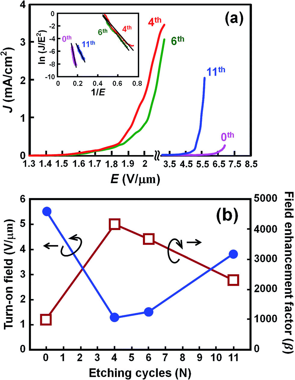 | ||
| Fig. 8 (a) Plots of field emission current density (J) versus applied electric field (E) for tapered Si nanostructure arrays fabricated with different number of the ACER cycles. The inset shows the corresponding Fowler–Nordheim plots. (b) Plots of turn-on field (E0) and field enhancement factor (β) of the tapered Si nanostructure arrays versus the number of the ACER cycles. | ||
The F–N equation can be rewritten as:
4. Conclusions
In summary, we successfully fabricated well-ordered arrays of vertically-aligned, needle-like and cone-like tapered Si nanostructures on (001)Si substrates by using the new approach combining the O2 plasma modified nanosphere lithography and Au-assisted catalytic etching and subsequently multiple ACER cycle process. The Ag-nanoparticle catalytic etching process occurred only at the upper part of Si nanowires due to the hydrophobic nature of the Si nanowire surfaces. After repeating the ACER cycle four or more times, the tip diameters of the produced Si nanowires were reduced from the original value of 120 nm to less than 10 nm. All the produced vertically-aligned tapered Si nanostructures were identified to be single crystalline with an axial orientation along the [001] direction, which was identical to the crystallographic orientation of the (001)Si wafers used. The field emission measurements also showed that the produced tapered Si nanostructures exhibited improved field emission characteristics compared to as-produced Si nanowires. The turn-on field value of the tapered Si nanowires after the 4th ACER cycle obtained in this study was found to be much lower than that of most Si-based nanostructures and other semiconductor nanostructures. The excellent field emission properties of long needle-like tapered Si nanowires make them very promising as high-performance field emitters. Furthermore, since the morphology and dimension of the top-ends of Si nanowires can be readily controlled by adjusting the ACER cycles, the simple versatile combined strategy proposed in this study makes the fabrication of a variety of periodic arrays of vertically-aligned, single crystalline tapered Si-based nanostructures viable.Acknowledgements
The research was supported by the Ministry of Science and Technology of Taiwan, R. O. C.References
- Y. C. Kim, S. H. Park, C. S. Lee, T. W. Chung, E. Cho, D. S. Chung and I. T. Han, Carbon, 2015, 91, 304 CrossRef CAS.
- L. Zhao, Y. X. Chen, Y. M. Liu, G. F. Zhang, J. C. She, S. Z. Deng, N. S. Xu and J. Chen, Curr. Appl. Phys., 2017, 17, 85 CrossRef.
- F. C. K. Au, K. W. Wong, Y. H. Tang, Y. F. Zhang, I. Bello and S. T. Lee, Appl. Phys. Lett., 1999, 75, 1700 CrossRef CAS.
- C. Mu, Y. X. Yu, W. Liao, X. S. Zhao, D. X. Chen and D. P. Yu, Appl. Phys. Lett., 2005, 87, 113104 CrossRef.
- D. C. Lim, H. S. Ahn, D. J. Choi, C. H. Wang and H. Tomokage, Surf. Coat. Technol., 2003, 168, 37 CrossRef CAS.
- R. D. Lawrowski, C. Prommesberger, C. Langer, F. Dams and R. Schreiner, Adv. Mater. Sci. Eng., 2014, 948708, 1 CrossRef.
- S. E. Huq, L. Chen and P. D. Prewett, Microelectron. Eng., 1995, 27, 95 CrossRef CAS.
- C. Li, G. J. Fang, S. Sheng, Z. Q. Chen, J. B. Wang, S. Ma and X. Z. Zhao, Phys. E, 2005, 30, 169 CrossRef CAS.
- V. Kumar, S. K. Saxena, V. Kaushik, K. Saxena, A. K. Shukla and R. Kumar, RSC Adv., 2014, 4, 5799 Search PubMed.
- Y. F. Tzeng, H. C. Wu, P. S. Sheng, N. H. Tai, H. T. Chiu, C. Y. Lee and I. N. Lin, ACS Appl. Mater. Interfaces, 2010, 2, 331 CAS.
- Z. P. Huang, H. Fang and J. Zhu, Adv. Mater., 2007, 19, 744 CrossRef CAS.
- K. Q. Peng, M. L. Zhang, A. Lu, N. B. Wong, R. Q. Zhang and S. T. Lee, Appl. Phys. Lett., 2007, 90, 163123 CrossRef.
- S. L. Cheng, C. Y. Chen and S. W. Lee, Thin Solid Films, 2010, 518, S190 CrossRef CAS.
- F. Teng, N. Li, L. X. Liu, D. Xu, D. Y. Xiao and N. Lu, RSC Adv., 2016, 6, 15803 RSC.
- H. P. Wang, K. Y. Lai, Y. R. Lin, C. A. Lin and J. H. He, Langmuir, 2010, 26, 12855 CrossRef CAS PubMed.
- T. Y. Hwang, G. H. An, J. H. Lim, N. V. Myung and Y. H. Choa, Jpn. J. Appl. Phys., 2014, 53, 05HA07 CrossRef.
- S. L. Cheng, C. H. Lo, C. F. Chuang and S. W. Lee, Thin Solid Films, 2012, 520, 3309 CrossRef CAS.
- L. Xu, W. Li, J. Xu, J. Zhou, L. C. Wu, X. G. Zhang, Z. Y. Ma and K. J. Chen, Appl. Surf. Sci., 2009, 255, 5414 CrossRef CAS.
- H. Y. Hsieh, S. H. Huang, K. F. Liao, S. K. Su, C. H. Lai and L. J. Chen, Nanotechnology, 2007, 18, 505305 CrossRef.
- S. S. Lv, Z. G. Li, S. M. Su, L. H. Lin, Z. J. Zhang and W. Miao, RSC Adv., 2014, 4, 31729 RSC.
- H. F. Hsu, J. Y. Wang and Y. H. Wu, J. Electrochem. Soc., 2014, 161, H53 CrossRef.
- H. Lin, H. Y. Cheung, F. Xiu, F. Y. Wang, S. P. Yip, N. Han, T. F. Hung, J. Zhou, J. C. Ho and C. Y. Wong, J. Mater. Chem. A, 2013, 1, 9942 CAS.
- J. Rybczynski, U. Ebels and M. Giersig, Colloids Surf., A, 2003, 219, 1 CrossRef CAS.
- A. B. D. Cassie, Discuss. Faraday Soc., 1948, 3, 11 RSC.
- S. K. Srivastava, D. Kumar, S. W. Schmitt, K. N. Sood, S. H. Christiansen and P. K. Singh, Nanotechnology, 2014, 25, 175601 CrossRef PubMed.
- K. Q. Peng, A. J. Lu, R. Q. Zhang and S. T. Lee, Adv. Funct. Mater., 2008, 18, 1 CrossRef.
- C. Y. Chen and C. P. Wong, Nanoscale, 2015, 7, 1216 RSC.
- Y. H. Cheng, C. K. Chou, C. Chen and S. Y. Cheng, Chem. Phys. Lett., 2004, 397, 17 CrossRef CAS.
- X. J. Huang, J. H. Lee, J. W. Lee, J. B. Yoon and Y. K. Choi, Small, 2008, 4, 211 CrossRef CAS PubMed.
- H. C. Wu, H. Y. Tsai, H. T. Chiu and C. Y. Lee, ACS Appl. Mater. Interfaces, 2010, 2, 3285 CAS.
- Y. M. Chang, P. H. Kao, H. M. Tai, H. W. Wang, C. M. Lin, H. Y. Lee and J. Y. Juang, Phys. Chem. Chem. Phys., 2013, 15, 10761 RSC.
- W. Li, J. Zhou, X. G. Zhang, J. Xu, L. Xu, W. M. Zhao, P. Sun, F. Q. Song, J. Q. Wan and K. J. Chen, Nanotechnology, 2008, 19, 135308 CrossRef PubMed.
- S. Ravipati, C. J. Kuo, J. Shieh, C. T. Chou and F. H. Ko, Microelectron. Reliab., 2010, 50, 1973 CrossRef CAS.
- J. H. Deng, L. Cheng, F. J. Wang, D. J. Li and G. A. Cheng, Mater. Lett., 2015, 138, 175 CrossRef CAS.
- S. K. Sahoo and A. Marikani, Nano, 2016, 11, 1650017 CrossRef CAS.
- C. M. Tang, Y. B. Wang, R. H. Yao, H. L. Ning, W. Q. Qiu and Z. W. Liu, Nanotechnology, 2016, 27, 395605 CrossRef CAS PubMed.
- C. M. Tang, X. Y. Liao, W. J. Zhong, H. Y. Yu and Z. W. Liu, RSC Adv., 2017, 7, 6439 RSC.
- R. C. Wang, C. P. Liu, J. L. Huang, S. J. Chen, Y. K. Tseng and S. C. Kung, Appl. Phys. Lett., 2005, 87, 013110 CrossRef.
- J. Rouhi, M. Alimanesh, S. Mahmud, R. A. Dalvand, C. H. Raymond Ooi and M. Rusop, Mater. Lett., 2014, 125, 147 CrossRef CAS.
- Z. Cuia, E. L. Li, W. Shi, D. M. Ma, T. Liu, X. Y. Liu, S. T. Lv, Q. H. I. Wang and G. H. Wu, Ceram. Int., 2015, 41, 6074 CrossRef.
- J. W. Zhao, Y. F. Zhang, Y. H. Li, C. H. Su, X. M. Song, H. Yan and R. Z. Wang, Sci. Rep., 2015, 5, 17692 CrossRef CAS PubMed.
- X. S. Fang, Y. S. Bando, U. K. Gautam, C. H. Ye and D. Golberg, J. Mater. Chem., 2008, 18, 509 RSC.
- H. Araki, T. Katayama and K. Yoshino, Appl. Phys. Lett., 2001, 79, 2636 CrossRef CAS.
- J. H. Deng, B. Yu, G. Z. Li, X. G. Hou, M. L. Zhao, D. J. Li, R. T. Zheng and G. A. Cheng, Nanoscale, 2013, 5, 12388 RSC.
- S. L. Wu, J. H. Deng, T. Zhang, R. T. Zheng and G. A. Cheng, Diamond Relat. Mater., 2012, 26, 83 CrossRef CAS.
| This journal is © The Royal Society of Chemistry 2017 |