
 Open Access Article
 This Open Access Article is licensed under a
 Creative Commons Attribution 3.0 Unported Licence
Thermoelectric properties of β-As, Sb and Bi monolayers†
Dong-Chen Zhang,
Ai-Xia Zhang,
San-Dong Guo* and
Yi-feng Duan
School of Physics, China University of Mining and Technology, Xuzhou 221116, Jiangsu, China. E-mail: guosd@cumt.edu.cn
First published on 5th May 2017
Abstract
Monolayer semiconductors of group-VA elements (As, Sb and Bi) with a graphene-like buckled structure offer the potential to achieve nanoscale electronic, optoelectronic and thermoelectric devices. Motivated by research on a recently-fabricated Sb monolayer (antimonene), we systematically investigate the thermoelectric properties of β-As, Sb and Bi monolayers by combining first-principles calculations and semiclassical Boltzmann transport theory. The generalized gradient approximation (GGA) plus spin–orbit coupling (SOC) is adopted for the electron part, and GGA is employed for the phonon part. It is found that SOC has important influences on the electronic structures, especially for Bi monolayers, that can induce observable SOC effects on the electronic transport coefficients. More specifically, SOC not only has detrimental influences on the electronic transport coefficients, but also produces enhanced effects. The calculated lattice thermal conductivity decreases gradually from the As to Bi monolayer, and the corresponding room-temperature sheet thermal conductance is 161.10 W K−1, 46.62 W K−1 and 16.02 W K−1 for the As, Sb and Bi monolayers, respectively, and these values can be converted into a common lattice thermal conductivity by dividing by the thickness of 2D material. The decreased thermal conductivity from As to Bi monolayer can be explained by the decreasing group velocities and phonon lifetimes. The sheet thermal conductance of the Bi monolayer is lower than that of other 2D materials, such as semiconducting transition-metal dichalcogenide monolayers and orthorhombic group IV–VI monolayers. A series of scattering times was employed to estimate the thermoelectric figure of merit, ZT. It is found that the n-type doped As and Bi monolayers have better thermoelectric properties than the p-type doped As and Bi monolayers, while a comparable ZT between the n- and p-type doped Bi monolayers is observed. Much higher ZT values can be obtained, provided that the electrical thermal conductivities are calculated using the Wiedemann–Franz law with L being constant. These results can stimulate further experimental works to open the new field for thermoelectric devices based on monolayers of group-VA elements.
I. Introduction
Due to its high mobility, heat conductance, and mechanical strength, graphene with a planar honeycomb structure is one of the most famous materials, but it lacks an intrinsic band gap, hindering its application in electronics and optoelectronics.1 The successful exfoliation of graphene has led to a large amount of research on other two-dimensional (2D) materials like silicene,2 germanene,3 phosphorene4 and transition-metal dichalcogenides,5 etc. Recently, monolayer semiconductors of group-VA elements (As, Sb, Bi) have been predicted to have good stability and intrinsic band gaps using first-principles calculations, and the graphene-like buckled structure (β-phase) was found to have the best stability.6 The Sb monolayer (antimonene) has been successfully exfoliated using micromechanical technology,7 and has been synthesized on various substrates via van der Waals epitaxial growth.8 Experimentally, it has been proven that Sb monolayers are highly stable under ambient conditions,7 and their high stability has been observed after aging in air for 30 days.8 Raman spectroscopy and transmission electron microscopy have shown that Sb monolayers have a graphene-like buckled structure.7,8 It is urgent and interesting to study the thermoelectric properties of Sb monolayers in detail, to determine whether they are potential thermoelectric materials.Thermoelectric materials, which can achieve direct hot-electricity conversion without moving parts, are of great interest in energy-related issues.9,10 The efficiency of thermoelectric conversion can be measured using the dimensionless figure of merit, ZT = S2σT/(κe + κL), in which S, σ, T, κe and κL are the Seebeck coefficient, electrical conductivity, working temperature, and the electronic and lattice thermal conductivities, respectively. It is believed that nanostructured materials, especially 2D materials, have potential application in highly efficient thermoelectric devices.11–15 The thermoelectric properties of semiconducting transition-metal dichalcogenide monolayers and orthorhombic group IV–VI monolayers have been widely investigated.16–21 Recently, our calculated results have shown that SOC can produce important effects on the electronic transport coefficients of various 2D materials,19,21–23 so it is necessary for the thermoelectric properties of 2D materials to include SOC. For group-VA monolayers, most of the research has been focused on their lattice thermal conductivities, and little research has been focused on their electronic transport properties. The lattice thermal conductivities of As and Sb monolayers with both graphene-like buckled and black phosphorene-like puckered honeycomb structures (α-phase) have been theoretically investigated.24–27 A highly anisotropic thermal conductivity along the zigzag and armchair directions is predicted for α-As and Sb monolayers.25,26 It has also been proven that chemical functionalization can make the κL value of Sb monolayers greatly decrease.27 The thermoelectric performance of α-As monolayers has been studied using Green’s function based transport techniques, including both the electron and phonon parts.28 The thermoelectric properties of β-Bi monolayers have also been studied, and the lattice thermal conductivity has been predicted via equilibrium molecular dynamics simulations.29 It is worth noting that a remarkable discrepancy between ref. 24 and 25 for the κL values of β-Sb monolayers has been found. This may be because a different thickness of the Sb monolayer was used, and the related discussion for the calculations of the transport coefficients of the 2D materials can be found in the next section (Computational details). It is interesting and necessary to systematically investigate the thermoelectric properties of β-As, Sb and Bi monolayers, including the electron and lattice parts. To compare the electrical conductivity, and electronic and lattice thermal conductivities of β-As, Sb and Bi monolayers, the same thickness should be used.
Here, we systematically investigate the thermoelectric properties of β-As, Sb and Bi monolayers using ab initio calculations in combination with Boltzmann transport equation formalism, including both the electron and phonon parts. SOC is considered for the electron part, which is very important for the electronic structures and transport coefficients of the β-As, Sb and Bi monolayers, especially for the Bi monolayers. The lattice thermal conductivities are calculated using the same thickness and sheet thermal conductances of the β-As, Sb and Bi monolayers, and they gradually decrease from As to Bi monolayers, which can be understood by the decreasing group velocities and phonon lifetimes. It is found that the sheet thermal conductance of Bi monolayers is lower than that of familiar 2D materials. Finally, the possible ZT is estimated using a series of empirical scattering times, which suggests that β-As, Sb and Bi monolayers may be potential 2D thermoelectric materials.
The rest of the paper is organized as follows. In the next section, we shall describe computational details about the first-principles and transport coefficients calculations. In the third section, we shall present the electronic structures and thermoelectric properties of the β-As, Sb and Bi monolayers. Finally, we shall give our discussions and conclusions in the fourth section.
II. Computational details
We use a full-potential linearized augmented-plane-wave method within density functional theory (DFT)30 to carry out calculations on the electronic structures of the β-As, Sb and Bi monolayers, as implemented in the package WIEN2k.31 The free atomic position parameters are optimized using the GGA of Perdew, Burke and Ernzerhof (GGA-PBE)32 with a force standard of 2 mRy per a.u. The SOC is included self-consistently,33–36 which gives rise to important influences on the electronic transport coefficients. The convergence results are determined using 5000 k-points in the first Brillouin Zone (BZ) for the self-consistent calculations, making a harmonic expansion up to 1max = 10 in each of the atomic spheres, and setting Rmt × kmax = 8 for the plane-wave cut-off. The self-consistent calculations are considered to be converged when the integration of the absolute charge-density difference between the input and output electron density is less than 0.0001|e| per formula unit, where e is the electron charge.Based on the results of the electronic structures, transport coefficients for the electron part are calculated through solving Boltzmann transport equations within the constant scattering time approximation (CSTA), as implemented in BoltzTrap,37 which shows reliable results in many classic thermoelectric materials.38–40 To obtain accurate transport coefficients, we set the parameter LPFAC to 20, and use at least 2408 k-points in the irreducible BZ for the energy band calculations. The lattice thermal conductivities are performed using Phono3py + VASP codes.41–44 The second order harmonic and third order anharmonic interatomic force constants are calculated using a 5 × 5 × 1 supercell and a 4 × 4 × 1 supercell, respectively. To compute the lattice thermal conductivities, the reciprocal spaces of the primitive cells are sampled using 50 × 50 × 2 meshes.
For 2D materials, the calculated electrical conductivity, and the electronic and lattice thermal conductivities depend on the length of the unit cell used in the calculations along the z direction,45 and so should be normalized by multiplying by Lz/d, where Lz is the length of the unit cell along the z direction and d is the thickness of 2D material, but the d value is not well defined. However, the dimensionless figure of merit ZT is independent of the length of unit cell used in the calculations along the z direction. In this work, the length of the unit cell used in our calculations along the z direction is used as the thickness of the β-As, Sb and Bi monolayers, and the corresponding d value is 18 Å. The thermal sheet conductance can be used as a fair comparison between various 2D monolayers, which can be obtained using κ × d.
III. Main calculated results and analysis
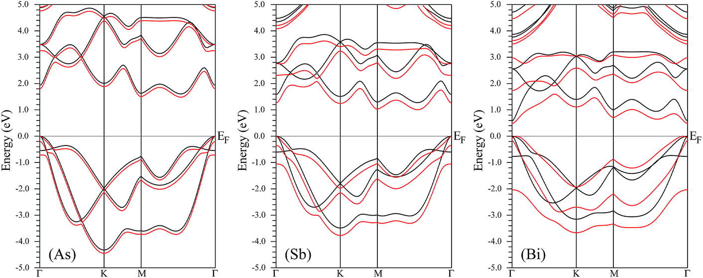
The β-phase of As, Sb and Bi monolayers is a graphene-like buckled honeycomb structure with a space group of P![[3 with combining macron]](https://www.rsc.org/images/entities/char_0033_0304.gif) m1 (no. 164), and the schematic crystal structure is shown in Fig. 1. The β-phase is different from the α-phase a with puckered honeycomb structure. The unit cell of the β-phase contains two atoms with each atom connected to three atoms of another plane, while the α-phase contains four atoms with each atom connected to two atoms of the same plane and one atom of another plane. In this work, the optimized lattice constants of the β-phase are used,6 and are summarized in Table 1. It is found that the buckling parameter h from Table 1, that is defined as the vertical distance separating the two atomic planes, gradually increases from the As to the Bi monolayer. The unit cells of the β-As, Sb and Bi monolayers are constructed with a vacuum region that is larger than 16 Å to avoid spurious interaction. As is well known, SOC has very important effects on the electronic structures and electronic transport coefficients of materials containing heavy elements,19–23 such as Bi. Firstly, the electronic structures of the β-As, Sb and Bi monolayers were investigated using GGA and GGA + SOC, and the energy band structures are plotted in Fig. 2 using GGA and GGA + SOC. The As and Sb monolayers were found to be indirect band gap semiconductors using both GGA and GGA + SOC, with a valence band maximum (VBM) at the Γ point and a conduction band minimum (CBM) at the M point. The Bi monolayer was found to be a direct band gap semiconductor using GGA, with a VBM and CBM at the Γ point, while it was found to be an indirect band gap semiconductor using GGA + SOC, with a VBM between the Γ and M points and a CBM at the Γ point. The GGA and GGA + SOC gaps, and the differences between them, are listed in Table 1. Both the GGA and GGA + SOC gaps decrease from the As to the Bi monolayer, and the difference for the Bi monolayer is less than that of the As and Sb monolayers, which is due to the change of the CBM from the M to Γ point. The three monolayers have some conduction band extrema (CBE) around the Fermi level, which is favorable for an n-type Seebeck coefficient. According to the SOC-induced changes of the outlines of the energy bands, the strength of the SOC increases from the As to Bi monolayer, which is consistent with their respective atomic mass. The representative spin–orbit splitting values at the high symmetry points Γ and K of the valence bands are summarized in Table 1. It is found that the spin–orbit splitting value at the K point can represent the strength of the SOC.
m1 (no. 164), and the schematic crystal structure is shown in Fig. 1. The β-phase is different from the α-phase a with puckered honeycomb structure. The unit cell of the β-phase contains two atoms with each atom connected to three atoms of another plane, while the α-phase contains four atoms with each atom connected to two atoms of the same plane and one atom of another plane. In this work, the optimized lattice constants of the β-phase are used,6 and are summarized in Table 1. It is found that the buckling parameter h from Table 1, that is defined as the vertical distance separating the two atomic planes, gradually increases from the As to the Bi monolayer. The unit cells of the β-As, Sb and Bi monolayers are constructed with a vacuum region that is larger than 16 Å to avoid spurious interaction. As is well known, SOC has very important effects on the electronic structures and electronic transport coefficients of materials containing heavy elements,19–23 such as Bi. Firstly, the electronic structures of the β-As, Sb and Bi monolayers were investigated using GGA and GGA + SOC, and the energy band structures are plotted in Fig. 2 using GGA and GGA + SOC. The As and Sb monolayers were found to be indirect band gap semiconductors using both GGA and GGA + SOC, with a valence band maximum (VBM) at the Γ point and a conduction band minimum (CBM) at the M point. The Bi monolayer was found to be a direct band gap semiconductor using GGA, with a VBM and CBM at the Γ point, while it was found to be an indirect band gap semiconductor using GGA + SOC, with a VBM between the Γ and M points and a CBM at the Γ point. The GGA and GGA + SOC gaps, and the differences between them, are listed in Table 1. Both the GGA and GGA + SOC gaps decrease from the As to the Bi monolayer, and the difference for the Bi monolayer is less than that of the As and Sb monolayers, which is due to the change of the CBM from the M to Γ point. The three monolayers have some conduction band extrema (CBE) around the Fermi level, which is favorable for an n-type Seebeck coefficient. According to the SOC-induced changes of the outlines of the energy bands, the strength of the SOC increases from the As to Bi monolayer, which is consistent with their respective atomic mass. The representative spin–orbit splitting values at the high symmetry points Γ and K of the valence bands are summarized in Table 1. It is found that the spin–orbit splitting value at the K point can represent the strength of the SOC.
 | ||
| Fig. 1 The crystal structures of the β-As, Sb and Bi monolayers: the top view (left) and the side view (right). | ||
| Name | a | h | G | Gso | G − Gso | ΓΔso | KΔso |
|---|---|---|---|---|---|---|---|
| As | 3.61 | 1.40 | 1.61 | 1.48 | 0.13 | 0.21 | 0.07 |
| Sb | 4.12 | 1.65 | 1.27 | 1.01 | 0.26 | 0.35 | 0.17 |
| Bi | 4.34 | 1.73 | 0.58 | 0.49 | 0.09 | 0.08 | 0.77 |
 | ||
| Fig. 2 The energy band structures of the β-As, Sb and Bi monolayers within GGA (black lines) and GGA + SOC (red lines). | ||
SOC can produce very important effects on the electronic transport coefficients in many 2D materials, such as semiconducting transition-metal dichalcogenide and orthorhombic group IV–VI monolayers.19–23 Firstly, the semi-classic transport coefficients are calculated using CSTA Boltzmann theory with GGA and GGA + SOC, and the doping effects are simulated by simply shifting the Fermi level into the conduction or valence bands within the rigid band approach, which is valid when the doping level is low.46–48 The Seebeck coefficient, S, the electrical conductivity with respect to the scattering time, σ/τ, the power factor with respect to the scattering time, S2σ/τ, and the electronic thermal conductivity with respect to the scattering time, κe/τ, as a function of doping level (N) at room temperature are plotted in Fig. 3 using GGA and GGA + SOC.
 | ||
| Fig. 3 The calculated transport coefficients of the β-As, Sb and Bi monolayers at room temperature (300 K) as a function of doping level (N) within GGA and GGA + SOC, including the Seebeck coefficient, S, the electrical conductivity with respect to the scattering time, σ/τ, the power factor with respect to the scattering time, S2σ/τ, and the electronic thermal conductivity with respect to the scattering time, κe/τ. | ||
For the As and Sb monolayers, it is found that SOC has a detrimental effect on the Seebeck coefficient in p-type doped ones, while it has a negligible influence in n-type doped ones. The detrimental effect can be explained by SOC-induced splitting at the Γ point, which reduces the degeneracy of the energy bands. However, the enhanced effect on the Seebeck coefficient (absolute value) can be observed in both n- and p-type doped Bi monolayers, which can be understood by band convergence.9 In the presence of SOC, the CBE along Γ–M and the CBM approach each other, which leads to an improved n-type Seebeck coefficient. When SOC is considered, the VBM changes from the Γ point to one point along Γ–M, and another valence band extremum (VBE) appears at one point along Γ–K. The VBE along Γ–K and VBM are very close, and the energy difference is only 0.0005 eV, which gives rise to an enhanced p-type Seebeck coefficient.
For n-type doping, the negligible SOC influence of the As and Sb monolayers on σ/τ can be observed, while a slightly improved effect for low p-type doping and a detrimental influence for high p-type doping can be achieved. A decreased effect on σ/τ caused by SOC in both n- and p-type doped Bi monolayers can be observed. The effect of the As and Sb monolayers on S2σ/τ that is induced by SOC has the same trend as the one on S. An enhanced effect on the S2σ/τ of Bi monolayers produced by SOC in n-type doping and a decreased influence in p-type doping can be fulfilled. It is found that the effect on κe/τ caused by SOC has almost a similar trend as the one on κe/τ that was not caused by SOC, which can be explained by the Wiedemann–Franz law: κe = LσT, in which L is the Lorenz number.
Based on the linearized phonon Boltzmann equation within the single-mode relaxation time approximation, the lattice thermal conductivities of the β-As, Sb and Bi monolayers can be attained, and are assumed to be independent of the doping level. Their phonon band structures are shown in Fig. 4, and agree well with previous results.6 Their unit cells contain two atoms, resulting in 3 acoustic and 3 optical phonon branches. From As to Bi monolayers, all of the branches move towards low energy, and the phonon dispersion becomes more localized. The maximal acoustic vibration frequency (MAVF) is 3.55 THz, 2.05 THz and 1.29 THz for the As, Sb and Bi monolayers, respectively, and a low MAVF beneficial to a low thermal conductivity. The width of the optical branches of the β-As, Sb and Bi monolayers is 2.71 THz, 1.58 THz and 1.08 THz, respectively, and the narrow width suggests there is little contribution to the thermal conductivity. The third optical branch has a larger dispersion than the first two, which means that the third one has a larger group velocity, leading to an obvious contribution to the lattice thermal conductivity. The phonon band gap decreases from As (2.79 THz) to Sb (2.39 THz) to Bi (1.82 THz) monolayers. It is found that the longitudinal acoustic (LA) and transverse acoustic (TA) branches are linear near the Γ point, while the z-direction acoustic (ZA) branch deviates from linearity near the Γ point, sharing the general feature of 2D materials.1,49 The related data are summarized in Table 2.
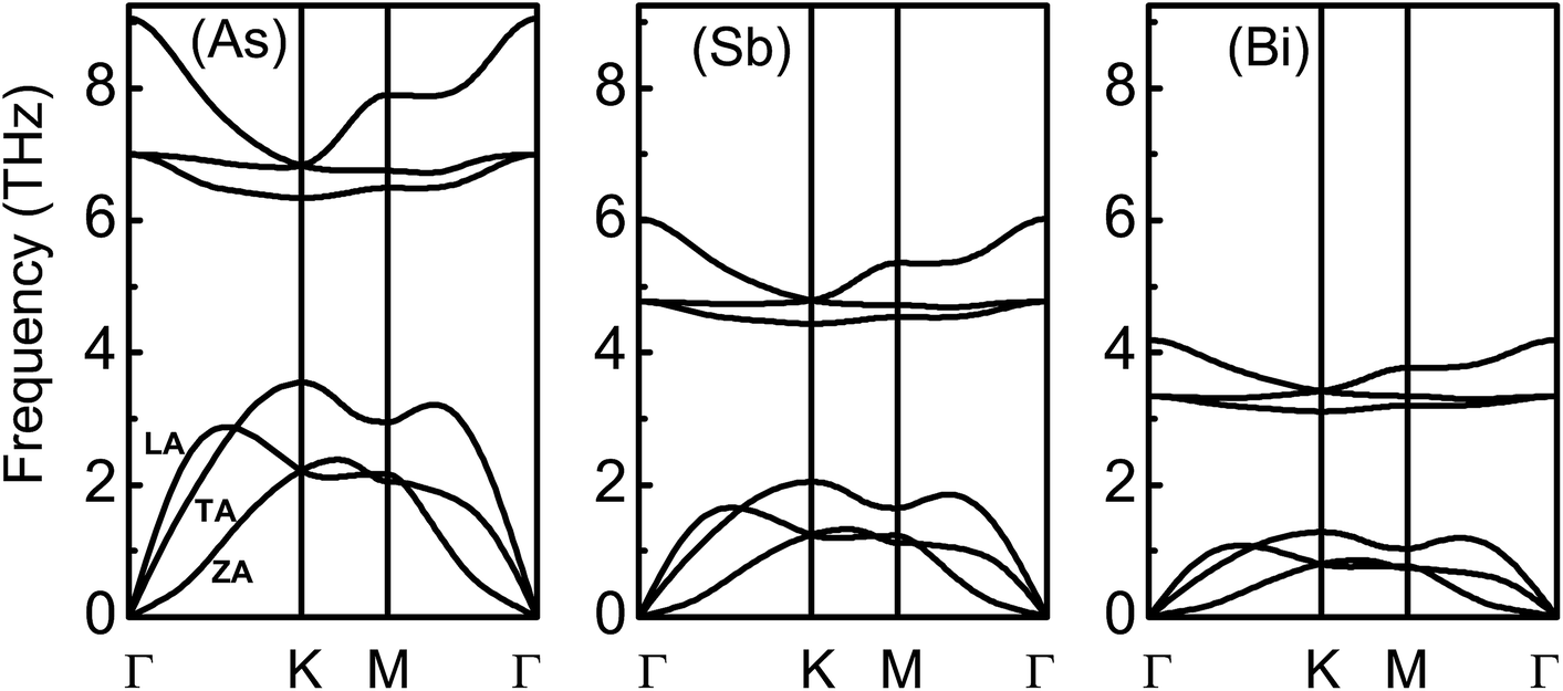 | ||
| Fig. 4 Phonon band structure of the β-As, Sb and Bi monolayers using GGA-PBE. | ||
| Name | MAVF | WO | PBG | TSC | ACL | FPD |
|---|---|---|---|---|---|---|
| As | 3.55 | 2.71 | 2.79 | 161.10 | 97.6 | 2.01 |
| Sb | 2.05 | 1.58 | 2.39 | 46.62 | 98.1 | 1.06 |
| Bi | 1.29 | 1.08 | 1.82 | 16.02 | 98.1 | 0.76 |
The lattice thermal conductivities of the β-As, Sb and Bi monolayers as a function of temperature are shown in Fig. 5, and the same thickness d (18 Å) is used. The room-temperature lattice thermal conductivity of the β-As, Sb and Bi monolayers is 8.95 W m−1 K−1, 2.59 W m−1 K−1 and 0.89 W m−1 K−1, respectively. To compare the lattice thermal conductivities of the various 2D materials, we converted all of the thermal conductivity values into thermal sheet conductance,45 and the corresponding thermal sheet conductance of the β-As, Sb and Bi monolayers was 161.10 W K−1, 46.62 W K−1 and 16.02 W K−1, respectively. At room temperature, a lattice thermal conductivity of 3.9 W m−1 K−1 for the Bi monolayer was predicted using equilibrium molecular dynamics simulations and a thickness of 4 Å,29 which is very close to our calculated value of 4.0 W m−1 K−1 with the same thickness. The thermal sheet conductance of the Bi monolayer is lower than that of other 2D materials (semiconducting transition-metal dichalcogenide and orthorhombic group IV–VI monolayers), and is very close to that of SnS (18.68 W K−1) and SnSe (17.55 W K−1).45 To examine the relative contributions of the acoustic modes to the total lattice thermal conductivity, the cumulative lattice thermal conductivity and the derivatives at room temperature are also plotted in Fig. 5. The acoustic branch of the β-As, Sb and Bi monolayers provides a contribution of 97.6%, 98.1% and 98.1%, respectively. This agrees with the usual picture that high-frequency optical phonons have a very small contribution to the thermal conductivity. The derivatives show that the change of the lattice thermal conductivity versus frequency has a peak value, and the corresponding frequency of the peak value is 2.01 THz, 1.16 THz and 0.76 THz for the β-As, Sb and Bi monolayers, respectively. These frequencies and cross values of ZA and LA branches almost overlap. Some key data are shown in Table 2. Furthermore, we examine the relative contributions of six phonon modes to the total lattice thermal conductivity. The mode lattice thermal conductivities are shown Table 3, and the percentages of the phonon modes contributions toward the total lattice thermal conductivity are plotted in Fig. 6. It is found that the TA branch provides the largest contribution in acoustic branches, and the third optical branch gives the greatest contribution in optical ones.
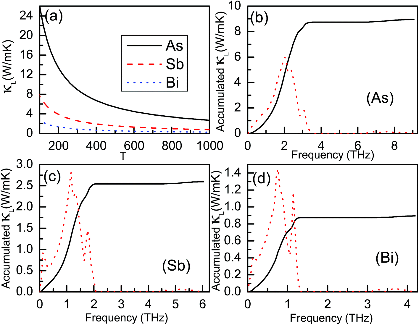 | ||
| Fig. 5 (a) The lattice thermal conductivities of the β-As, Sb and Bi monolayers as a function of temperature using GGA-PBE. (b–d) The accumulated lattice thermal conductivities of the β-As, Sb and Bi, and the derivatives. | ||
| Name | ZA | TA | LA | O1 | O2 | O3 | κL |
|---|---|---|---|---|---|---|---|
| As | 2.927 | 3.109 | 2.702 | 0.032 | 0.013 | 0.169 | 8.952 |
| Sb | 0.630 | 1.086 | 0.826 | 0.009 | 0.001 | 0.043 | 2.594 |
| Bi | 0.247 | 0.360 | 0.266 | 0.004 | 0.001 | 0.016 | 0.894 |
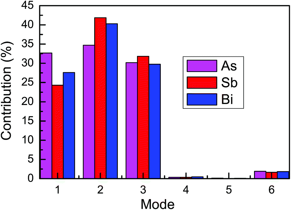 | ||
| Fig. 6 Phonon modes contributions towards the total lattice thermal conductivity in the β-As, Sb and Bi monolayers; (1) represents the ZA branch, (2) represents the TA branch, (3) represents the LA branch and (4–6) represent the optical branches. | ||
According to Fig. 7, the group velocity of the ZA branch is smaller than that of the LA and TA branches, which is due to the nonlinear dispersion of the ZA branch near the Γ point. Similar results can also be found in other 2D materials such as graphene, silicene, germanene and stanene.50 It is clearly seen that the group velocities become small from the As to the Bi monolayer, which leads to a decreasing thermal conductivity. The largest group velocity for the ZA, TA and LA branches near the Γ point is 0.73 km s−1, 3.03 km s−1 and 4.62 km s−1 for the As monolayer, 0.42 km s−1, 2.08 km s−1 and 3.24 km s−1 for the Sb monolayer, and 0.34 km s−1, 1.42 km s−1 and 2.26 km s−1 for the Bi monolayer. The lattice thermal conductivity and the phonon lifetimes are nearly proportional to each other from the single-mode relaxation time method.44 The phonon lifetimes of the β-As, Sb and Bi monolayers at room temperature are plotted in Fig. 7. As can be seen, most of the phonon lifetimes decrease from the As to Bi monolayers, which can explain the decreasing lattice thermal conductivity. It is found that optical phonon lifetimes are much shorter than the acoustic ones, which suggests that the optical branches have little contribution to the lattice thermal conductivity. The anharmonic interactions can be described by mode Grüneisen parameters, and a low lattice thermal conductivity can be produced by strong anharmonicity with large Grüneisen parameters. The mode Grüneisen parameters of the β-As, Sb and Bi monolayers in the irreducible Brillouin zone at room temperature are plotted in Fig. 8. It is found that the mode Grüneisen parameters of the β-As, Sb and Bi monolayers are comparable to each other. So, the decreasing thermal conductivity from the As to the Bi monolayer can be attributed to decreasing group velocities and phonon lifetimes.
 | ||
| Fig. 7 Calculated phonon group velocities and phonon lifetimes of the β-As, Sb and Bi monolayers in the irreducible Brillouin zone using GGA-PBE; (1) represents the ZA branch, (2) represents the TA branch, (3) represents the LA branch and (4–6) represent the optical branches. | ||
 | ||
| Fig. 8 Calculated mode Grüneisen parameters of the β-As, Sb and Bi monolayers in the irreducible Brillouin zone using GGA-PBE; (1) represents the ZA branch, (2) represents the TA branch, (3) represents the LA branch and (4–6) represent the optical branches. | ||
Based on the calculated electron and phonon transport coefficients, the figure of merit, ZT, can be attained to estimate the efficiency of the thermoelectric conversion. Firstly, the power factor with respect to the scattering time, S2σ/τ, and the electronic thermal conductivity with respect to the scattering time, κe/τ , versus the doping level (N) using GGA + SOC at 300 and 600 K are plotted in Fig. 9. However, another unknown quantity is the scattering time, τ, but it is difficult to calculate the scattering time from first-principles calculations due to the complexity of the various carrier scattering mechanisms. Here, 1 × 10⁻¹⁵ s, 1 × 10⁻¹⁴ s and 1 × 10⁻¹³ s are used to attain the power factor and electronic thermal conductivity. According to the obtained power factor, electronic thermal conductivity and lattice thermal conductivity from Fig. 5, the possible ZT of the β-As, Sb and Bi monolayers as a function of doping level at 300 and 600 K are plotted in Fig. 10. It is found that ZT increases with increased scattering time, τ, which can be explained by the relation: ZT = ZTe/(κe + κL), in which ZTe = S2σT/κe as an upper limit of ZT. The κe value can be obtained using κe/τr × τ, in which τr and τ are the true and empirical scattering time, respectively. As the scattering time, τ, increases, the κe increases. That leads to a κe/(κe + κL) value that is closer to one, and then ZT is closer to ZTe. The calculated results show the As and Sb monolayers with n-type doping have a better ZT than those with p-type doping, and that the Bi monolayer shows almost an equivalent ZT when it is n- and p-type doped. It is found that a peak ZT in n-type doped monolayers is up to 0.40, 0.62 and 0.60 for the As, Sb and Bi monolayers, respectively, with a classic scattering time τ = 10−14 s, and the corresponding doping level gradually decreases. These results imply that the β-As, Sb and Bi monolayers may be potential 2D thermoelectric materials when the doping is optimized.
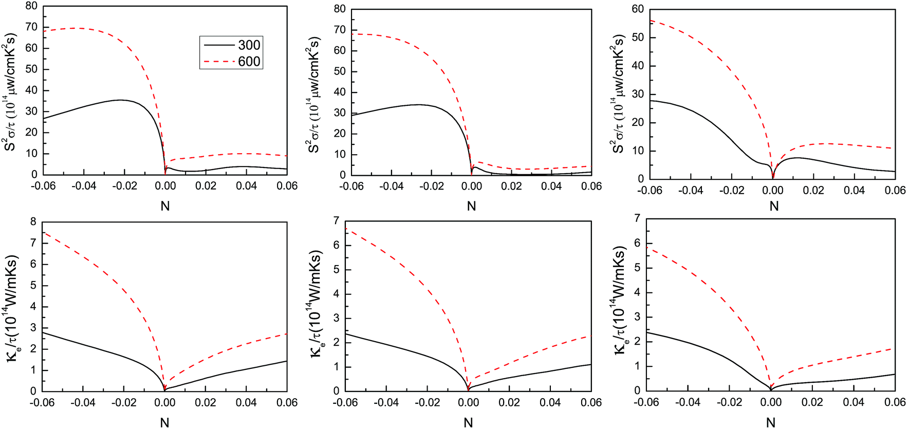 | ||
| Fig. 9 At 300 and 600 K, the power factor with respect to the scattering time, S2σ/τ, and the electronic thermal conductivity with respect to the scattering time, κe/τ , versus the doping level (N) using GGA + SOC. | ||
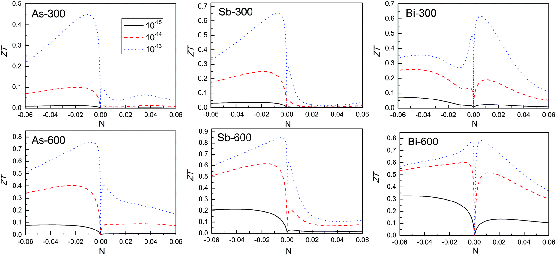 | ||
| Fig. 10 At 300 and 600 K, the calculated ZT of the β-As, Sb and Bi monolayers as a function of doping level using three scattering times τ: 1 × 10⁻¹⁵ s, 1 × 10⁻¹⁴ s and 1 × 10⁻¹³ s. The electrical thermal conductivities are obtained from the outputs of BoltzTrap. | ||
Much higher ZT values for 2D materials have been reported.29,51 In these calculations, the electrical thermal conductivities are calculated using the Wiedemann–Franz law: κe = LσT, with L being a constant with a value of 1.5 × 10⁻⁸ W Ω K−2 for monolayer SnSe51 and 2.38 × 10⁻⁸ W Ω K−2 for monolayer Bi.29 In our calculations, the electrical thermal conductivities are used from the outputs of BoltzTrap, and the used value of L depends on the temperature and the doping level. Here, the electrical thermal conductivities are also calculated using the Wiedemann–Franz law with L being 2.38 × 10⁻⁸ W Ω K−2, and the ZT values of the β-As, Sb and Bi monolayers are recalculated. The possible ZT values of the β-As, Sb and Bi monolayers as a function of doping level at 600 K are shown in Fig. 11. It is clearly seen that very high ZT values can be obtained.
 | ||
| Fig. 11 At 600 K, the calculated ZT of the β-As, Sb and Bi monolayers as a function of doping level using three scattering times τ: 1 × 10⁻¹⁵ s, 1 × 10⁻¹⁴ s and 1 × 10⁻¹³ s. The electrical thermal conductivities are calculated using the Wiedemann–Franz law. | ||
IV. Discussions and conclusions
The Seebeck coefficient can be tuned by removing or enhancing band degeneracy, and furthermore can affect the power factor. For the β-As, Sb and Bi monolayers, the SOC not only removes band degeneracy (orbital degeneracy), but also enhances it (valley degeneracy). The SOC can lead to reduced effects on the p-type Seebeck coefficient of As and Sb monolayers by lifting the degeneracy of the Γ point, but can enhance the Seebeck coefficient of Bi monolayers as the bands converge, which is caused by spin–orbit splitting. Similar SOC effects on the Seebeck coefficient are also found in semiconducting transition-metal dichalcogenide monolayers MX2 (M = Zr, Hf, Mo, W and Pt; X = S, Se and Te).23 The enhanced effects on the Seebeck coefficient can be observed in monolayers WX2 (X = S, Se and Te), and the detrimental effects can be observed in MX2 (M = Zr, Hf, Mo and Pt; X = S, Se and Te). For bulk materials, the detrimental effects on Seebeck coefficient caused by SOC can also be found in Mg2X (X = Si, Ge and Sn)52,53 and half-Heusler ANiB (A = Ti, Hf, Sc and Y; B = Sn, Sb and Bi).54 Therefore, including SOC is very important for the electronic transport coefficients of the β-As, Sb and Bi monolayers.The electronic structures of 2D materials are quite sensitive to strain, and the β-As, Sb and Bi monolayers have some CBE around their Fermi levels. So, it is possible to tune their thermoelectric properties using band engineering. Strain (pressure) has been proven to be a very effective strategy to improve the thermoelectric properties of 2D (bulk) materials.19,22,53,55 For bulk Mg2Sn, pressure can induce accidental degeneracies (orbital degeneracy) of CBM, which can significantly improve the power factor.53 A strain-enhanced power factor can also be found in monolayer MoS2,22 PtSe2 (ref. 19) and ZrS2 (ref. 55) due to band convergence (valley degeneracy) induced by strain. It has also been proven that tensile strain can reduce the lattice thermal conductivity in many 2D materials, such as PtSe2 (ref. 19) and ZrS2.55 It has been predicted that strain can induce band convergence in As monolayers.56 Therefore, the strain effects on the thermoelectric properties of the β-As, Sb and Bi monolayers are well worth studying. It has been predicted using first-principles calculations that a perpendicular electric field can induce an indirect-to-direct gap transition in the As monolayer at 4.2 V nm−1,56 which suggests that the electric field can also tune the electronic structure. Therefore, it is possible to tune the electronic transport properties of the β-As, Sb and Bi monolayers using an electric field.
The potential thermoelectric materials should possess low lattice thermal conductivity. To compare the lattice thermal conductivities of the different monolayer 2D materials, the same thickness d should be adopted, or the sheet thermal conductance should be used.45 Here, the same thickness of the interlayer distance of graphite (3.35 Å) was used.45 The lattice thermal conductivities and sheet thermal conductances of the β-As, Sb and Bi monolayers, some semiconducting transition-metal dichalcogenide monolayers and orthorhombic group IV–VI monolayers are summarized in Table 4. The lattice thermal conductivity of the Bi monolayer is lower than that of the orthorhombic group IV–VI monolayers and semiconducting transition-metal dichalcogenide monolayers, which suggests that it may be a potential 2D thermoelectric material compared to other familiar 2D materials. The lattice thermal conductivity of the Sb monolayer has been widely calculated, and the values obtained include 15.1 W m−1 K−1,24 13.8 W m−1 K−1 (ref. 25) and 2.3 W m−1 K−1.27 This apparent contradiction may be because a different thickness was used to calculate the lattice thermal conductivity.
| Name | GeS | GeSe | SnS | SnSe | ZrS2 | ZrSe2 | HfS2 | HfSe2 | As | Sb | Bi |
|---|---|---|---|---|---|---|---|---|---|---|---|
| A | 15.80 | 9.43 | 5.58 | 5.24 | 23.25 | 18.55 | 29.06 | 20.71 | 48.09 | 13.74 | 4.78 |
| B | 52.93 | 31.58 | 18.68 | 17.55 | 77.89 | 62.14 | 97.35 | 69.38 | 161.10 | 46.62 | 16.02 |
In conclusion, we have carried out detailed theoretical studies of the thermoelectric properties of β-As, Sb and Bi monolayers based on ab initio calculations combined with Boltzman transport theory. It is shown that SOC has important effects on the electronic properties of the β-As, Sb and Bi monolayers, and these effects have been ignored in other theoretical calculations.6,56 The sheet thermal conductance is used to compare the lattice thermal conductivities of the different 2D materials. The decreased thermal conductivity from the As to the Bi monolayers is due to the decreasing group velocities and phonon lifetimes. The sheet thermal conductance of the Bi monolayer is lower than that of other well-studied 2D materials, and is very favorable for realizing a high thermoelectric efficiency. Finally, a series of hypothetical scattering times were adopted to estimate the possible efficiency of thermoelectric conversion. If the electrical thermal conductivities are calculated using the Wiedemann–Franz law, with L being constant, much higher ZT values can be obtained. Our work suggests that these β-As, Sb and Bi monolayers with a graphene-like buckled structure may offer a new 2D playground to achieve high-performance thermoelectric devices.
Acknowledgements
The work is sponsored by the Fundamental Research Funds for the Central Universities under Grant No. 2015XKMS081. We are grateful to the Advanced Analysis and Computation Center of CUMT for the award of CPU hours to accomplish this work.References
- A. H. Castro Neto, F. Guinea, N. M. R. Peres, K. S. Novoselov and A. K. Geim, Rev. Mod. Phys., 2009, 81, 109–162 CrossRef CAS.
- B. Aufray, A. Kara, S. Vizzini, H. Oughaddou, C. Landri, B. Ealet and G. L. Lay, Appl. Phys. Lett., 2010, 96, 183102 CrossRef.
- L. Li, Y. Yu, G. J. Ye, Q. Ge, X. Ou, H. Wu, D. Feng, X. H. Chen and Y. Zhang, Nat. Nanotechnol., 2014, 9, 372–377 CrossRef CAS PubMed.
- H. Liu, A. T. Neal, Z. Zhu, Z. Luo, X. Xu, D. Tomnek and P. D. Ye, ACS Nano, 2014, 8, 4033–4041 CrossRef CAS PubMed.
- G. Cunningham, M. Lotya, C. S. Cucinotta, S. Sanvito, S. D. Bergin, R. Menzel, M. S. P. Shaffer and J. N. Coleman, ACS Nano, 2012, 6, 3468–3480 CrossRef CAS PubMed.
- S. Zhang, M. Xie, F. Li, Z. Yan, Y. Li, E. Kan, W. Liu, Z. Chen and H. Zeng, Angew. Chem., 2016, 128, 1698–1701 CrossRef.
- P. Ares, F. Aguilar-Galindo, D. Rodrguez-San-Miguel, D. A. Aldave, S. Daz-Tendero, M. Alcam, F. Martn, J. Gmez-Herrero and F. Zamora, Adv. Mater., 2016, 28, 6332–6336 CrossRef CAS PubMed.
- J. Ji, X. Song, J. Liu, Z. Yan, C. Huo, S. Zhang, M. Su, L. Liao, W. Wang, Z. Ni, Y. Hao and H. Zeng, Nat. Commun., 2016, 7, 13352 CrossRef CAS PubMed.
- Y. Pei, X. Shi, A. LaLonde, H. Wang, L. Chen and G. J. Snyder, Nature, 2011, 473, 66–69 CrossRef CAS PubMed.
- A. D. LaLonde, Y. Pei, H. Wang and G. Jeffrey Snyder, Mater. Today, 2011, 14, 526–532 CrossRef CAS.
- L. D. Hicks and M. S. Dresselhaus, Phys. Rev. B: Condens. Matter Mater. Phys., 1993, 47, 12727–12731 CrossRef CAS.
- L. D. Hicks, T. C. Harman and M. S. Dresselhaus, Appl. Phys. Lett., 1993, 63, 3230–3232 CrossRef CAS.
- Y. Xu, Z. Li and W. Duan, Small, 2014, 10, 2182–2199 CrossRef CAS PubMed.
- J. P. Heremans, M. S. Dresselhaus, L. E. Bell and D. T. Morelli, Nat. Nanotechnol., 2013, 8, 471–473 CrossRef CAS PubMed.
- M. Dresselhaus, G. Chen, M. Tang, R. Yang, H. Lee, D. Wang, Z. Ren, J.-P. Fleurial and P. Gogna, Adv. Mater., 2007, 19, 1043–1053 CrossRef CAS.
- S. Kumar and U. Schwingenschlgl, Chem. Mater., 2015, 27, 1278–1284 CrossRef CAS.
- J. Wu, H. Schmidt, K. K. Amara, X. Xu, G. Eda and B. zyilmaz, Nano Lett., 2014, 14, 2730–2734 CrossRef CAS PubMed.
- Z. Jin, Q. Liao, H. Fang, Z. Liu, W. Liu, Z. Ding, T. Luo and N. Yang, Sci. Rep., 2015, 5, 18342 CrossRef CAS PubMed.
- S.-D. Guo, J. Mater. Chem. C, 2016, 4, 9366–9374 RSC.
- F. Q. Wang, S. Zhang, J. Yu and Q. Wang, Nanoscale, 2015, 7, 15962–15970 RSC.
- S.-D. Guo and Y.-H. Wang, J. Appl. Phys., 2017, 121, 034302 CrossRef.
- S.-D. Guo, Comput. Mater. Sci., 2016, 123, 8–13 CrossRef CAS.
- S.-D. Guo and J.-L. Wang, Semicond. Sci. Technol., 2016, 31, 095011 CrossRef.
- S. Wang, W. Wang and G. Zhao, Phys. Chem. Chem. Phys., 2016, 18, 31217–31222 RSC.
- G. Zheng, Y. Jia, S. Gao and S.-H. Ke, Phys. Rev. B: Condens. Matter Mater. Phys., 2016, 94, 155448 CrossRef.
- M. Zeraati, S. M. Vaez Allaei, I. Abdolhosseini Sarsari, M. Pourfath and D. Donadio, Phys. Rev. B: Condens. Matter Mater. Phys., 2016, 93, 085424 CrossRef.
- T. Zhang, Y.-Y. Qi, X.-R. Chen and L.-C. Cai, Phys. Chem. Chem. Phys., 2016, 18, 30061–30067 RSC.
- L. Medrano Sandonas, D. Teich, R. Gutierrez, T. Lorenz, A. Pecchia, G. Seifert and G. Cuniberti, J. Phys. Chem. C, 2016, 120, 18841–18849 CAS.
- L. Cheng, H. Liu, X. Tan, J. Zhang, J. Wei, H. Lv, J. Shi and X. Tang, J. Phys. Chem. C, 2014, 118, 904–910 CAS.
- P. Hohenberg and W. Kohn, Phys. Rev., 1964, 136, B864–B871 CrossRef.
- G. K. H. M. D. K. P. Blaha, K. Schwarz and J. Luitz, WIEN2k, an Augmented Plane Wave+ Local Orbitals Program for Calculating Crystal Properties, Karlheinz Schwarz Technische Universität Wien, Austria, 2001 Search PubMed.
- J. P. Perdew, K. Burke and M. Ernzerhof, Phys. Rev. Lett., 1996, 77, 3865–3868 CrossRef CAS PubMed.
- A. H. MacDonald, W. E. Picket and D. D. Koelling, J. Phys. C: Solid State Phys., 1980, 13, 2675 CrossRef CAS.
- D. J. Singh and L. Nordstrom, Plane Waves, Pseudopotentials and the LAPW Method, Springer, New York, 2nd edn, 2006 Search PubMed.
- J. Kunes, P. Novk, R. Schmid, P. Blaha and K. Schwarz, Phys. Rev. B: Condens. Matter Mater. Phys., 2001, 64, 153102 CrossRef.
- D. D. Koelling and B. N. Harmon, J. Phys. C: Solid State Phys., 1977, 10, 3107 CrossRef CAS.
- G. K. Madsen and D. J. Singh, Comput. Phys. Commun., 2006, 175, 67–71 CrossRef CAS.
- B.-L. Huang and M. Kaviany, Phys. Rev. B: Condens. Matter Mater. Phys., 2008, 77, 125209 CrossRef.
- L. Xu, Y. Zheng and J.-C. Zheng, Phys. Rev. B: Condens. Matter Mater. Phys., 2010, 82, 195102 CrossRef.
- J. J. Pulikkotil, D. J. Singh, S. Auluck, M. Saravanan, D. K. Misra, A. Dhar and R. C. Budhani, Phys. Rev. B: Condens. Matter Mater. Phys., 2012, 86, 155204 CrossRef.
- G. Kresse, J. Non-Cryst. Solids, 1995, 192–193, 222–229 CrossRef.
- G. Kresse and J. Furthmuller, Comput. Mater. Sci., 1996, 6, 15–50 CrossRef CAS.
- G. Kresse and D. Joubert, Phys. Rev. B: Condens. Matter Mater. Phys., 1999, 59, 1758–1775 CrossRef CAS.
- A. Togo, L. Chaput and I. Tanaka, Phys. Rev. B: Condens.Matter Mater. Phys., 2015, 91, 094306 CrossRef.
- X. Wu, V. Varshney, J. Lee, Y. Pang, A. K. Roy and T. Luo, Chem. Phys. Lett., 2017, 669, 233–237 CrossRef CAS.
- T. J. Scheidemantel, C. Ambrosch-Draxl, T. Thonhauser, J. V. Badding and J. O. Sofo, Phys. Rev. B: Condens. Matter Mater. Phys., 2003, 68, 125210 CrossRef.
- G. K. H. Madsen, J. Am. Chem. Soc., 2006, 128, 12140–12146 CrossRef CAS PubMed.
- X. Gao, K. Uehara, D. D. Klug, S. Patchkovskii, J. S. Tse and T. M. Tritt, Phys. Rev. B: Condens. Matter Mater. Phys., 2005, 72, 125202 CrossRef.
- H. Zabel, J. Phys.: Condens. Matter, 2001, 13, 7679 CrossRef CAS.
- B. Peng, H. Zhang, H. Shao, Y. Xu, G. Ni, R. Zhang and H. Zhu, Phys. Rev. B: Condens. Matter Mater. Phys., 2016, 94, 245420 CrossRef.
- F. Q. Wang, S. Zhang, J. Yu and Q. Wang, Nanoscale, 2015, 7, 15962–15970 RSC.
- K. Kutorasinski, B. Wiendlocha, J. Tobola and S. Kaprzyk, Phys. Rev. B: Condens. Matter Mater. Phys., 2014, 89, 115205 CrossRef.
- S.-D. Guo and J.-L. Wang, RSC Adv., 2016, 6, 31272–31276 RSC.
- S.-D. Guo, J. Alloys Compd., 2016, 663, 128–133 CrossRef CAS.
- H. Y. Lv, W. J. Lu, D. F. Shao, H. Y. Lu and Y. P. Sun, J. Mater. Chem. C, 2016, 4, 4538–4545 RSC.
- C. Kamal and M. Ezawa, Phys. Rev. B: Condens. Matter Mater. Phys., 2015, 91, 085423 CrossRef.
Footnote |
| † PACS numbers: 72.15.Jf, 71.20.-b, 71.70.Ej, 79.10.-n. |
| This journal is © The Royal Society of Chemistry 2017 |