
 Open Access Article
 This Open Access Article is licensed under a
 Creative Commons Attribution 3.0 Unported Licence
First-principles study on intrinsic defects of SnSe
Yucheng Huang *a,
Chan Wanga,
Xi Chena,
Danmei Zhoua,
Jinyan Dua,
Sufan Wanga and
Lixing Ning*b
*a,
Chan Wanga,
Xi Chena,
Danmei Zhoua,
Jinyan Dua,
Sufan Wanga and
Lixing Ning*b
aCenter for Nano Science and Technology, College of Chemistry and Material Science, The Key Laboratory of Functional Molecular Solids, Ministry of Education, Anhui Laboratory of Molecule-Based Materials, Anhui Normal University, Wuhu, 241000, Peoples' Republic of China. E-mail: huangyc@mail.ahnu.edu.cn
bAnhui Province Key Laboratory of Optoelectric Materials Science and Technology, Department of Physics, Anhui Normal University, Wuhu, 241000, Peoples' Republic of China. E-mail: ninglx@mail.ahnu.edu.cn
First published on 24th May 2017
Abstract
The formation energies and electronic properties of intrinsic defects of SnSe, including two vacancies (VSn and VSe), two interstitials (Sni and Sei) and two antisites (SnSe and SeSn), are investigated by using density functional theory (DFT) calculations. The results indicate that, due to a relatively low formation energy as well as a desirable ultra-shallow transition energy level, VSn can act as an effective source for p-type conduction under both Sn- and Se-rich conditions, which implies that SnSe is a native p-type semiconductor. On the other hand, a native n-type conduction is unlikely to be realized due to the absence of effective intrinsic sources. In addition, all the three types of intrinsic defects are not capable of inducing magnetism.
1. Introduction
As an abundant, inexpensive and environmental friendly material, tin(II) selenide has shown intriguing physical properties and wide applications in the fields of infrared optoelectronic devices, phase-change alloys for electronic memory,1 and cathodic materials for rechargeable lithium batteries.2 The structure of this important binary IV–VI group semiconductor compound crystallizes in a cubic rocksalt phase with space group Fm![[3 with combining macron]](https://www.rsc.org/images/entities/char_0033_0304.gif) m or in an orthorhombic phase with space group Pmna. The two phases are comparable in thermodynamic stability and the former has been identified as a new topological crystalline insulator material.3,4 The structure of latter is similar to phosphorene5,6 and is recognized as a highly distorted NaCl lattice.7 Importantly, this kind of layered SnSe has a direct band gap of 1.3 eV and an indirect band gap of 0.9 eV, falling within the range of the optimum band gap for solar cells (1.0–1.5 eV),8 which makes orthorhombic SnSe an excellent candidate for application in solar cells.9–11 This has resulted in extensive studies on its synthesis and properties during recent decades.12–19 Recently, intensive interest has been devoted to the doping of foreign species in the layered SnSe, which has been shown to greatly improve electronic, magnetic and thermoelectric properties of the material.7,20–25 For example, Leng et al.23 reported that the carrier density in AgxSn1−xSe compounds was dramatically increased by substituting Sn with Ag. Wei and coworkers26 found that the carrier concentration and electrical conductivity in p-type polycrystalline SnSe were significantly enhanced in the presence of alkali metals (Li, Na and K), among which Na displayed the best doping efficiency along with excellent thermoelectric properties. Interestingly, the first report on the thermoelectric properties of iodine-doped n-type SnSe polycrystalline demonstrated that the highest figure of merit ZT = 0.8 can be achieved at about 773 K and alloying with SnS can lead to an increase of ZT to 1.0.27 A very recent study reported that the presence of cubic rock-salt-type precipitate phase contributes significantly to the enhancement of electrical conductivity without the introduction of dopants.28
m or in an orthorhombic phase with space group Pmna. The two phases are comparable in thermodynamic stability and the former has been identified as a new topological crystalline insulator material.3,4 The structure of latter is similar to phosphorene5,6 and is recognized as a highly distorted NaCl lattice.7 Importantly, this kind of layered SnSe has a direct band gap of 1.3 eV and an indirect band gap of 0.9 eV, falling within the range of the optimum band gap for solar cells (1.0–1.5 eV),8 which makes orthorhombic SnSe an excellent candidate for application in solar cells.9–11 This has resulted in extensive studies on its synthesis and properties during recent decades.12–19 Recently, intensive interest has been devoted to the doping of foreign species in the layered SnSe, which has been shown to greatly improve electronic, magnetic and thermoelectric properties of the material.7,20–25 For example, Leng et al.23 reported that the carrier density in AgxSn1−xSe compounds was dramatically increased by substituting Sn with Ag. Wei and coworkers26 found that the carrier concentration and electrical conductivity in p-type polycrystalline SnSe were significantly enhanced in the presence of alkali metals (Li, Na and K), among which Na displayed the best doping efficiency along with excellent thermoelectric properties. Interestingly, the first report on the thermoelectric properties of iodine-doped n-type SnSe polycrystalline demonstrated that the highest figure of merit ZT = 0.8 can be achieved at about 773 K and alloying with SnS can lead to an increase of ZT to 1.0.27 A very recent study reported that the presence of cubic rock-salt-type precipitate phase contributes significantly to the enhancement of electrical conductivity without the introduction of dopants.28
It was appreciated that lattice defects will be present in the material under various growth conditions, including native and exotic defects. The presence of these undesired defects could have significant effects on electronic, magnetic and optical properties of the material. Moreover, native defects could also be accompanied with chemical impurities.29 In this light, the influence of native defects should be taken into account when interpreting experimental results for material properties. To the best of our knowledge, however, no systematic investigation on the native defects in the bulk SnSe has been reported until now. Thus, there is a great need to understand the basic characteristics associated with these defects.
In the present work, we have performed DFT calculations on two vacancies (VSn and VSe), two interstitials (Sni and Sei), and two antisites (SnSe and SeSn) with a supercell approach. The defect formation energies, electronic and magnetic properties of these defects have been investigated. The results show that an intrinsic p-type semiconductor can be derived from VSn in bulk SnSe under both Sn- and Se-rich conditions, whereas n-type conduction is difficult to achieve. No magnetism can be induced by all three types of intrinsic defects.
2. Computational methods and models
The first-principle DFT calculations were performed with the projector augmented wave (PAW)30 pseudopotentials as implemented in the Vienna Ab Initio Simulation Package (VASP).31–33 The generalized gradient approximation (GGA) with Perdew–Burke–Ernzerhof (PBE)34,35 functional was adopted to model the exchange and correlation interactions. The lattice parameters and internal ion coordinates were fully relaxed using a conjugate gradient algorithm with a force tolerance of 0.01 eV Å−1, and electronic convergence threshold for energy was set to be 10−5 eV. Although a standard GGA approach would underestimate the band gap, the other properties are hardly changed as demonstrated in a recent study.36 The Monkhorst–Pack37 k-point mesh of 3 × 5 × 5 was employed in the first Brillouin-zone for the structural optimizations while a 3 × 8 × 8 mesh was used to calculate electronic properties. A denser 6 × 10 × 10 k-mesh was also used to calculate the band gap and the result only deviates by a fraction of meV from that obtained using a 3 × 8 × 8 one. The cutoff energy for the plane-wave basis was 350 eV which has been proved to be sufficient enough to give converged result.8 To determine the ground magnetic state, all systems have been examined by spin-polarized calculations.As seen in Fig. 1a, SnSe has a double-layered geometrical structure, and the Sn and Se atoms are connected with a zigzag pattern at the same plane. The optimized lattice parameters of bulk SnSe are a = 11.64, b = 4.22 and c = 4.49 Å, which are in agreement with the experimental values (a = 11.55, b = 4.16, and c = 4.45 Å).1 The corresponding bond lengths of Sn–Se were calculated to be 2.78 and 2.83 Å (Fig. 1a), which also agree well with those reported in ref. 8. In order to minimize the spurious defect–defect interactions, a 1 × 3 × 3 unit cell consisting of 36 Sn and 36 Se atoms was constructed from the bulk. Native defects were introduced by excavating one Sn/Se atom (VSn/VSe), embedding one Sn/Se atom (Sni/Sei) and substituting one Sn/Se atom with an antisite atom (SnSe/SeSn) (Fig. 1b). All the studied defects are proved to be the most stable one. The defect–defect distances in yz plane and x directions are at least 11.6 Å, giving a reasonable approximation of the isolated defects. To evaluate the effect of supercell size, a larger 2 × 4 × 4 supercell was constructed. First, the formation energies of vacancy defect VSn are calculated to be 1.53 (Sn-rich) and 0.80 eV (Se-rich), respectively, which are slightly larger than those using a 1 × 3 × 3 supercell (1.47 and 0.73 eV, see text). Second, the calculated transition level ε(0/2−) of VSn is nearly 0 eV, which is also close to the result obtained from a 1 × 3 × 3 supercell (0.004 eV, see text). Obviously, these differences are within the error range of DFT. Note that, besides the neutral states, all point defects considered in this work are also charged in the range from q = −2 to +2.
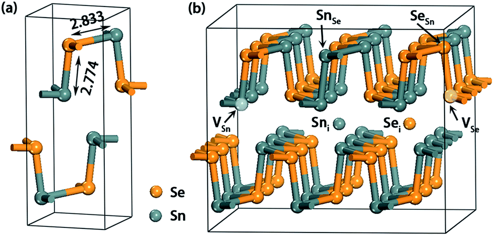 | ||
| Fig. 1 (a) The geometric structure of bulk SnSe with the selected bond lengths (in Å) indicated. (b) The 1 × 3 × 3 SnSe supercell structure with six intrinsic point defects under investigation is illustrated. | ||
3. Results and discussion
3.1 Electronic properties of the pristine SnSe
Before the analysis of native defects, we first investigate the electronic structure of pristine SnSe. As shown in Fig. 2a, SnSe has a band gap of 0.65 eV at the PBE level, which is smaller than the experimental value (0.9 eV).38 Nevertheless, a band gap of 1.1 eV was obtained when the Heyd–Scuseria–Ernzerhof (HSE06)39 screened hybrid functional was used (Fig. 2b). These results are in accordance with the previously reported values at the same computational level.8,40 It can be seen from Fig. 2c that the lower energy valence bands in the range from −4.0 to −2.0 eV are ascribed to the interaction between Sn-5p and Se-4p states. At variance, Sn-5s and Sn-5p states interact with Se-4p states in the upper valence bands, resulting in the formation of anti-bonding states.41 Moreover, the conduction band is mainly contributed by Sn-5p and Se-4p states, and Sn-5s states have almost no contribution to the conduction band minimum (CBM).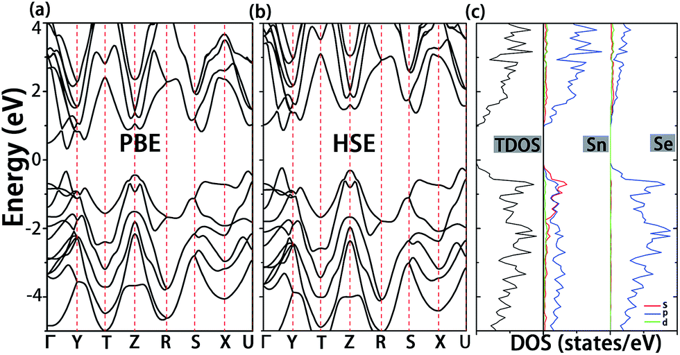 | ||
| Fig. 2 Calculated band structures of the pristine SnSe at the DFT-PBE and HSE06 level are illustrated in (a) and (b), respectively. The corresponding densities of states (DOS) of the pristine SnSe by HSE06 calculation are shown in (c) and the panels from left to right are the total density of states (TDOS) and the partial density of states (PDOS) for the Sn and Se atom, respectively. | ||
3.2 Determination of the upper and lower limit of chemical potential
For the calculations of defect formation energies and thermodynamic transition levels, we have simulated two different preparation conditions for these intrinsic defects, including Sn-rich (Se-poor) and Se-rich (Sn-poor). First, the chemical potential of Sn or Se must be less than its natural phase to avoid the formation of hcp Sn or Se crystal. As shown in Fig. 3, the upper limits for Sn and Se are indicated by vertical and parallel lines, respectively. The growth of the SnSe crystal is expected to be homogeneous if the chemical potentials of Sn and Se atoms vary within the following constraint condition,| μSnSe = μSn + μSe | (1) |
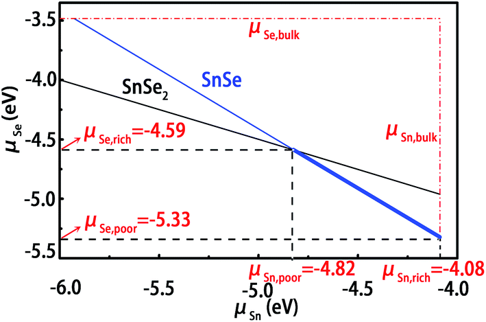 | ||
| Fig. 3 Thermodynamic growth condition of SnSe crystal. The horizontal and vertical dot-dashed lines represent the upper limit of Se and Sn chemical potentials determined by the natural phases of Sn and Se, respectively. The blue and black solid lines depict the equilibrium growth conditions of SnSe and SnSe2, respectively. The range of allowable growth conditions of SnSe crystal is labelled by the bold solid line. | ||
Moreover, when considering alternative phases, we must set more strict limitations on the chemical potentials under thermal equilibrium growth conditions. For SnSe, another phase of SnSe2 may coexist in the system. Compared with SnSe, the atomic ration of Se to Sn is higher, which indicates that the SnSe2 phase tends to grow effectively under the Se-rich growth conditions. In order to suppress the formation of such an unwanted phase, the growth conditions must be restricted below the upper limit value of μSe. In thermodynamic equilibrium for SnSe2, the chemical potentials of Sn and Se atoms must satisfy the following constraint condition
| μSnSe2 = μSn + 2μSe | (2) |
3.3 Defect formation energy
Generally, the stabilities of different defect structures are always estimated by the calculation of the formation energy. The formation energy (ΔHD,q) of a defect (D) in a charge state q is defined as:42
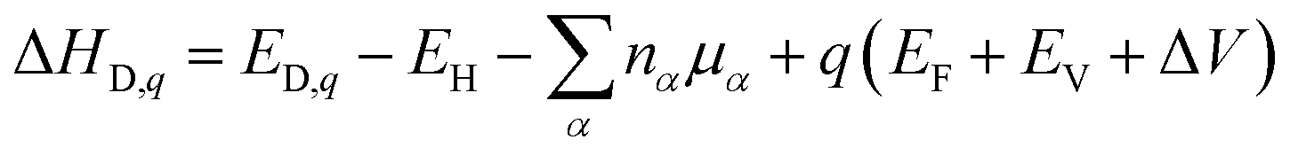 | (3) |
The formation energies of the intrinsic point defects in different charge states are listed in Table 1. We have removed the values with formation energies larger than 1.5 eV from the table, since these values mean low formation probabilities of the corresponding defects. As seen in Table 1, under Sn-rich condition, the three defects in their neutral charge states (SnSe, VSn and VSe) have the potential to affect SnSe electrical properties due to their relatively low formation energies (<1.5 eV). Under Se-rich condition, the formation energies of the neutral vacancies are still relatively low. It is interesting to observe that different preparation conditions have different effects on the formation energies: VSe, Sni and SnSe have lower formation energies under Sn-rich condition, but under Se-rich condition, the formation energies of VSn, Sei and SeSn become lower instead. Therefore, compared with cation-poor condition, cation interstitials and anion vacancies are more energetically favorable under the anion-poor condition. On the contrary, anion interstitials and cation vacancies are prone to be formed under the cation-poor condition. Similar findings have been reported in the studies of native defects in ZnO47 and SnS.48
| Defects | q | EF (Sn-rich) | EF (Se-rich) |
|---|---|---|---|
| VSn | 2− | 1.47 | 0.73 |
| 1− | 1.42 | 0.69 | |
| 0 | 1.47 | 0.73 | |
| VSe | 2− | 1.95 | 2.68 |
| 1− | 1.02 | 1.75 | |
| 0 | 0.16 | 0.89 | |
| 1+ | −0.23 | 0.51 | |
| Sni | 0 | 2.48 | 3.22 |
| 1+ | 1.73 | 2.47 | |
| 2+ | 1.17 | 1.91 | |
| Sei | 2− | 5.22 | 4.49 |
| 1− | 4.28 | 3.55 | |
| 0 | 3.41 | 2.67 | |
| 1+ | 3.24 | 2.50 | |
| SnSe | 2− | 1.75 | 3.22 |
| 1− | 1.11 | 2.58 | |
| 0 | 0.62 | 2.09 | |
| 1+ | 0.39 | 1.86 | |
| 2+ | 0.17 | 1.65 | |
| SeSn | 2− | 4.11 | 2.64 |
| 0 | 3.41 | 1.94 | |
| 1+ | 3.21 | 1.74 | |
| 2+ | 3.15 | 1.68 |
Defects often introduce levels in the band gap or near the band edge.49 The transition level of a defect is the Fermi level position where the defect can donate/accept electrons. Deep level means that removing an electron or hole from the trap to the valance or conduction band requires relative high energy. The transition level ε(q/q′) is defined as the Fermi level position for which the formation energies of a defect in charge states q is equal to that in charge state q′, which can be expressed as42
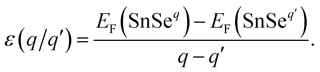 | (4) |
Fig. 4a and b present the calculated formation energies of the six fundamental intrinsic defects in SnSe as a function of the Fermi level (EF) under the Sn- and Se-rich conditions, respectively. Here the charged states from q = −2 to +2 are considered for the charged defects since the nominal valence of Sn/Se in a perfect SnSe is Sn2+/Se2−. For vacancies, under both conditions, it can be easily identified that VSn with q = −2 has the lowest formation energy among all kinds of intrinsic defects and a desirable ultra-shallow transition energy level ε(0/2−) located very closely to the VBM. This indicates that VSn can act as a shallow acceptor which is likely to make a prominent contribution to p-type conduction. With the increase of hole carriers concentration, EF will move downward and then stay on the crossing point between VSn (q = −2) and VSe (q = 0) (VSe(q = +1)) under Sn-rich (Se-rich) condition (Fig. 4). In view of the fact that VSn is more energetically favorable than VSe under the Se-rich condition, this condition is thereby favorable for the formation of VSn. Nevertheless, it is also important to be aware of the formation of other Se-rich phase like SnSe2 during the growth. Thus, manipulating the growth condition not toward Se-rich too much is required for preventing the formation of SnSe2 phase. Similar to VSn, VSe also has the relative low formation energy under both growth conditions. However, the transition energy level ε(1+/0) is closer to the VBM rather than the CBM, such that the VSe defect is in a stable neutral charge state at high EF (≥0.384 eV) and acts as a deep donor. Accordingly, VSe is predicted to have an insignificant effect on n-type conduction. For the case of antisite defects, the transition energy level ε(1+/0) of SnSe lies far away from the CBM, which means that it will become positively ionized only when Fermi level is in the low energy region EF ≤ 0.237, and thus SnSe acts as a deep donor and is excluded from appropriate candidates for p-type conduction. SeSn is a deep acceptor with a high positive formation energy, which indicates SeSn is not an effective source for n-type conduction. In terms of interstitial defects, the donor defect Sni has a high transition energy level ε(1+/0) with respect to the CBM, however the high positive formation energies of Sni under both conditions indicate that this shallow donor defect is unlikely to form, with minor contribution to n-type conduction. Sei can act as an acceptor but it has an ultra-deep transition energy level which is localized extremely near the edge of CBM. Moreover, this defect is energetically unfavorable and thus its contribution to the p-type conduction may be ignored. Although the contribution to n-type conduction could be expected, due to the relative low ε(1+/0) transition level with respect to the VBM, the thermodynamic instability determines that it is not the main source (Table 2).
 | ||
| Fig. 4 The calculated formation energies of intrinsic defects in SnSe as a function of Fermi level (EF) under the Sn-rich (a) and Se-rich conditions (b). The band gap value is the one calculated by DFT-HSE06 method. | ||
| Defects | q/q′ | ε(q/q′) (eV) |
|---|---|---|
| VSn | 2−/0 | 0.004 |
| VSe | 0/1− | 0.86 |
| 1+/0 | 0.38 | |
| Sni | 1+/0 | 0.75 |
| 2+/1+ | 0.56 | |
| Sei | 0/1− | 0.87 |
| 1+/0 | 0.17 | |
| SnSe | 1−/2− | 0.64 |
| 0/1− | 0.48 | |
| 1+/0 | 0.24 | |
| 2+/1+ | 0.21 | |
| SeSn | 0/2− | 0.35 |
| 1+/0 | 0.20 | |
| 2+/1+ | 0.06 |
From the above analysis, we can conclude that no intrinsic defect can act as an effective source for n-type conduction under both growth conditions. On the other hand, p-type conduction can be easily achieved by introducing VSn in SnSe, which suggests that SnSe is an intrinsic p-type semiconductor. This result agrees well with the reported observations that the bulk SnSe exhibits a p-type conductivity with hole mobilities up to 10−3 cm2 V−1 s−1 along the c axis.50,51
3.4 Electronic properties of intrinsic defects
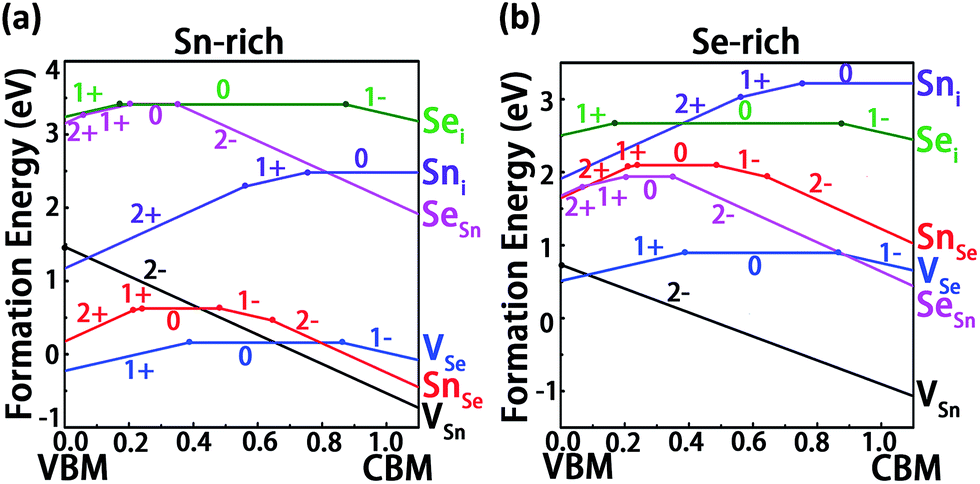
To further validate the above conclusions, the effects of intrinsic defects on electronic and magnetic properties of SnSe have also been studied. Spin-polarized calculations were first carried out to examine whether the intrinsic defects can induce magnetisms into the system. Unlike versatile magnetic properties of GaS52 and MoS2 (ref. 53) monolayers induced by native defects, no magnetism was found for the intrinsic defects in SnSe, which is evidenced by the observation that the DOSs for the majority and minority spin channels are symmetrical (Fig. 5). For the Sn vacancy, the DOS near the valance band are mainly contributed by Se-4p states. Meanwhile, Sn-5p states play an important role in the states near the CBM. The Fermi level shifts toward the valance band, rendering the material a p-type characteristic. For VSe, a small narrow peak appears around the VBM which is mainly contributed by Sn-5p states. The VSe defect is a deep donor as indicated above, thus it is not an effective source for n-type conduction. For the case of antisite defects, SnSe acts as a deep donor while SeSn acts as a deep acceptor. In the case of interstitial defects, an extra Sn atom causes the concentration of electrons to increase, resulting in an upward movement of EF. It is clearly seen that the DOS near the CBM are mainly contributed by Sn-4p states, with minor contribution from Sn-4s. Sni defect could act as a shallow donor, but the high formation energy excluded its role in p-type conduction. On the other hand, as seen from Fig. 5, both the ε(1+/0) and ε(0/1−) transition levels of the Sei are far from the CBM and VBM, thus failing to contribute the n- and p-type conductivities. | ||
| Fig. 5 Calculated TDOSs and PDOSs for the intrinsic defects (VSn, VSe, Sni, Sei, SnSe and SeSn) in SnSe (at the PBE level). The panels from top to bottom are the TDOS, PDOS of the nearest Sn atom and Se atom to the defect position, respectively. The s, p and d orbitals are marked up with red, blue and green lines, respectively. The vertical lines show the position of EF. | ||
It is worth noting that the long range van der Waals interactions maybe play a pivotal role in the layered structure. Therefore, the PBE-D3 method54 including the dispersion interaction between two layers is carefully checked. The PBE-D3 optimized lattice parameters (a = 11.64, b = 4.21 and c = 4.49 Å) are essentially the same to those by PBE one, and the calculated band gap of bulk SnSe is 0.66 eV, also close to the corresponding PBE value. To further validate the effect on other conclusion we made, we choose VSn to recalculate its transition levels. Our results showed that the ε(0/2−) of VSn is 0.02 eV, demonstrating that adding “D” has minor effect on the main conclusions. In fact, previous studies48,55 regarding on intrinsic defects of the same layered materials also ignored the dispersion effect.
4. Conclusion
In conclusion, the formation energies, electronic and magnetic properties of six intrinsic defects in SnSe were systematically investigated on the basis of DFT. It was shown that VSn is able to make a prominent contribution to the p-type conduction under both Sn- and Se-rich conditions due to its relatively lower formation energy and a desirable ultra-shallow thermodynamic transition level. By contrast, intrinsic n-type conduction was difficult to achieve since no effective sources were found. Our results also revealed that all intrinsic defects are unable to induce magnetism. Overall, this work provides a good start to the realization of p-type conduction in SnSe in the absence of impurities.Acknowledgements
This work was supported by National Natural Science Foundation of China No. 21573002 (H. Y.), 11574003 (N. L) and 21373012 (W. S.). The numerical calculations in this paper have been done on the super-computing system in the Supercomputing Center of University of Science and Technology of China.References
- M. A. Franzman, C. W. Schlenker, M. E. Thompson and R. L. Brutchey, J. Am. Chem. Soc., 2010, 132, 4060–4061 CrossRef CAS PubMed.
- J. Ning, G. Xiao, T. Jiang, L. Wang, Q. Dai, B. Zou, B. Liu, Y. Wei, G. Chen and G. Zou, CrystEngComm, 2011, 13, 4161–4166 RSC.
- Y. Sun, Z. Zhong, T. Shirakawa, C. Franchini, D. Li, Y. Li, S. Yunoki and X.-Q. Chen, Phys. Rev. B: Condens. Matter Mater. Phys., 2013, 88, 235122 CrossRef.
- Z. Wang, J. Wang, Y. Zang, Q. Zhang, J.-A. Shi, T. Jiang, Y. Gong, C.-L. Song, S.-H. Ji, L.-L. Wang, L. Gu, K. He, W. Duan, X. Ma, X. Chen and Q.-K. Xue, Adv. Mater., 2015, 27, 4150–4154 CrossRef CAS PubMed.
- G. Shi and E. Kioupakis, J. Appl. Phys., 2015, 117, 065103 CrossRef.
- T. Chattopadhyay, J. Pannetier and H. Von Schnering, J. Phys. Chem. Solids, 1986, 47, 879–885 CrossRef CAS.
- S. Chen, K. Cai and W. Zhao, Phys. B, 2012, 407, 4154–4159 CrossRef CAS.
- Y. Huang, C. Ling, H. Liu and S. Wang, RSC Adv., 2014, 4, 6933–6938 RSC.
- W. J. Baumgardner, J. J. Choi, Y.-F. Lim and T. Hanrath, J. Am. Chem. Soc., 2010, 132, 9519–9521 CrossRef CAS PubMed.
- S. Liu, X. Guo, M. Li, W.-H. Zhang, X. Liu and C. Li, Angew. Chem., Int. Ed., 2011, 50, 12050–12053 CrossRef CAS PubMed.
- P. D. Antunez, J. J. Buckley and R. L. Brutchey, Nanoscale, 2011, 3, 2399–2411 RSC.
- A. J. Hong, L. Li, H. X. Zhu, Z. B. Yan, J. M. Liu and Z. F. Ren, J. Mater. Chem. A, 2015, 3, 13365–13370 CAS.
- S. Zhao, H. Wang, Y. Zhou, L. Liao, Y. Jiang, X. Yang, G. Chen, M. Lin, Y. Wang, H. Peng and Z. Liu, Nano Res., 2015, 8, 288–295 CrossRef CAS.
- K.-M. Chung, D. Wamwangi, M. Woda, M. Wuttig and W. Bensch, J. Appl. Phys., 2008, 103, 083523 CrossRef.
- L.-D. Zhao, S.-H. Lo, Y. Zhang, H. Sun, G. Tan, C. Uher, C. Wolverton, V. P. Dravid and M. G. Kanatzidis, Nature, 2014, 508, 373–377 CrossRef CAS PubMed.
- L. Li, Z. Chen, Y. Hu, X. Wang, T. Zhang, W. Chen and Q. Wang, J. Am. Chem. Soc., 2013, 135, 1213–1216 CrossRef CAS PubMed.
- B. Nariya, A. Dasadia, M. Bhayani, A. Patel and A. Jani, Chalcogenide Lett., 2009, 6, 549–554 CAS.
- C. W. Li, J. Hong, A. F. May, D. Bansal, S. Chi, T. Hong, G. Ehlers and O. Delaire, Nat. Phys., 2015, 11, 1063–1065 CrossRef CAS.
- Y. C. Huang, X. Chen, C. Wang, L. Peng, Q. Qian and S. F. Wang, Nanoscale, 2017 10.1039/C7NR01952A.
- Y. Huang, C. Ling, Z. Fang and S. Wang, Phys. E, 2014, 59, 102–106 CrossRef CAS.
- E. K. Chere, Q. Zhang, K. Dahal, F. Cao, J. Mao and Z. Ren, J. Mater. Chem. A, 2016, 4, 1848–1854 CAS.
- Q. Wang, W. Yu, X. Fu, C. Qiao, C. Xia and Y. Jia, Phys. Chem. Chem. Phys., 2016, 18, 8158–8164 RSC.
- H. Leng, M. Zhou, J. Zhao, Y. Han and L. Li, J. Electron. Mater., 2016, 45, 527–534 CrossRef CAS.
- K. Peng, X. Lu, H. Zhan, S. Hui, X. Tang, G. Wang, J. Dai, C. Uher, G. Wang and X. Zhou, Energy Environ. Sci., 2016, 9, 454–460 CAS.
- N. K. Singh, S. Bathula, B. Gahtori, K. Tyagi, D. Haranath and A. Dhar, J. Alloys Compd., 2016, 668, 152–158 CrossRef CAS.
- T.-R. Wei, G. Tan, X. Zhang, C.-F. Wu, J.-F. Li, V. P. Dravid, G. J. Snyder and M. G. Kanatzidis, J. Am. Chem. Soc., 2016, 138, 8875–8882 CrossRef CAS PubMed.
- Q. Zhang, E. K. Chere, J. Sun, F. Cao, K. Dahal, S. Chen, G. Chen and Z. Ren, Adv. Energy Mater., 2015, 5, 1500360 CrossRef.
- G. Tang, Q. Wen, T. Yang, Y. Cao, W. Wei, Z. Wang, Z. Zhang and Y. Li, RSC Adv., 2017, 7, 8258–8263 RSC.
- S. Na-Phattalung, M. F. Smith, K. Kim, M.-H. Du, S.-H. Wei, S. B. Zhang and S. Limpijumnong, Phys. Rev. B: Condens. Matter Mater. Phys., 2006, 73, 125205 CrossRef.
- P. E. Blöchl, Phys. Rev. B: Condens. Matter Mater. Phys., 1994, 50, 17953–17979 CrossRef.
- G. Kresse and J. Hafner, Phys. Rev. B: Condens. Matter Mater. Phys., 1994, 49, 14251–14269 CrossRef CAS.
- G. Kresse and J. Hafner, Phys. Rev. B: Condens. Matter Mater. Phys., 1993, 47, 558–561 CrossRef CAS.
- G. Kresse and J. Furthmüller, Comput. Mater. Sci., 1996, 6, 15–50 CrossRef CAS.
- J. P. Perdew and Y. Wang, Phys. Rev. B: Condens. Matter Mater. Phys., 1992, 45, 13244–13249 CrossRef.
- J. P. Perdew, J. A. Chevary, S. H. Vosko, K. A. Jackson, M. R. Pederson, D. J. Singh and C. Fiolhais, Phys. Rev. B: Condens. Matter Mater. Phys., 1992, 46, 6671–6687 CrossRef CAS.
- S. Prada, L. Giordano and G. Pacchioni, J. Phys. Chem. C, 2013, 117, 9943–9951 CAS.
- H. J. Monkhorst and J. D. Pack, Phys. Rev. B: Solid State, 1976, 13, 5188–5192 CrossRef.
- I. Lefebvre, M. A. Szymanski, J. Olivier-Fourcade and J. C. Jumas, Phys. Rev. B: Condens. Matter Mater. Phys., 1998, 58, 1896–1906 CrossRef CAS.
- J. Heyd, G. E. Scuseria and M. Ernzerhof, J. Chem. Phys., 2006, 124, 219906 CrossRef.
- L. C. Gomes and A. Carvalho, Phys. Rev. B: Condens. Matter Mater. Phys., 2015, 92, 085406 CrossRef.
- J. Yang, G. Zhang, G. Yang, C. Wang and Y. X. Wang, J. Alloys Compd., 2015, 644, 615–620 CrossRef CAS.
- C. G. Van de Walle and J. Neugebauer, J. Appl. Physiol., 2004, 95, 3851–3879 CrossRef CAS.
- C. Persson, Y.-J. Zhao, S. Lany and A. Zunger, Phys. Rev. B: Condens. Matter Mater. Phys., 2005, 72, 035211 CrossRef.
- D. B. Laks, C. G. Van de Walle, G. F. Neumark, P. E. Blöchl and S. T. Pantelides, Phys. Rev. B: Condens. Matter Mater. Phys., 1992, 45, 10965–10978 CrossRef CAS.
- S. B. Zhang and J. E. Northrup, Phys. Rev. Lett., 1991, 67, 2339–2342 CrossRef CAS PubMed.
- S.-H. Wei, Comput. Mater. Sci., 2004, 30, 337–348 CrossRef CAS.
- A. Janotti and C. G. Van de Walle, Phys. Rev. B: Condens. Matter Mater. Phys., 2007, 76, 165202 CrossRef.
- Z. Xiao, F.-Y. Ran, H. Hosono and T. Kamiya, Appl. Phys. Lett., 2015, 106, 152103 CrossRef.
- Y. Huang, D. Zhou, X. Chen, H. Liu, C. Wang and S. Wang, ChemPhysChem, 2016, 17, 375–379 CrossRef CAS PubMed.
- H. Maier and D. R. Daniel, J. Electron. Mater., 1977, 6, 693–704 CrossRef CAS.
- J.-i. Umeda, J. Phys. Soc. Jpn., 1961, 16, 124–125 CrossRef CAS.
- H. Chen, Y. Li, L. Huang and J. Li, RSC Adv., 2015, 5, 50883–50889 RSC.
- D. Cao, H. B. Shu, T. Q. Wu, Z. T. Jiang, Z. W. Jiao, M. Q. Cai and W. Y. Hu, Appl. Surf. Sci., 2016, 361, 199–205 CrossRef CAS.
- S. Grimme, J. Antony, S. Ehrlich and H. Krieg, J. Chem. Phys., 2010, 132, 154104 CrossRef PubMed.
- A. Togo, F. Oba, I. Tanaka and K. Tatsumi, Phys. Rev. B: Condens. Matter Mater. Phys., 2006, 74, 195128 CrossRef.
| This journal is © The Royal Society of Chemistry 2017 |